Abstract
Superjunction (SJ) technology offers a promising solution to the challenges faced by silicon carbide (SiC) Metal Oxide Semiconductor Field-Effect Transistors (MOSFETs) operating at high voltages (>3 kV). However, the fabrication of SJ devices presents significant challenges due to fabrication complexity. This paper presents a comprehensive analysis of a feasible and easy-to-fabricate semi-superjunction (SSJ) design for 3.3 kV SiC MOSFETs. The proposed approach utilizes trench etching and sidewall implantation, with a tilted trench to facilitate the implantation process. Through Technology Computer-Aided Design (TCAD) simulations, we investigate the effects of the p-type sidewall on the charge balance and how it affects key performance characteristics, such as breakdown voltage (BV) and on-state resistance (RDS-ON). In particular, both planar gate (PSSJ) and trench gate (TSSJ) designs are simulated to evaluate their performance improvements over conventional planar MOSFETs. The PSSJ design achieves a 2.5% increase in BV and a 48.7% reduction in RDS-ON, while the TSSJ design further optimizes these trade-offs, with a 3.1% improvement in BV and a significant 64.8% reduction in RDS-ON compared to the benchmark. These results underscore the potential of tilted trench SSJ designs to significantly enhance the performance of SiC SSJ MOSFETs for high-voltage power electronics while simplifying fabrication and lowering costs.
1. Introduction
Silicon carbide (SiC) Metal Oxide Semiconductor Field-Effect Transistors (MOSFETs) offer several advantages over traditional silicon (Si) devices due to the superior properties of the material, including a higher breakdown electric field, superior thermal conductivity, faster switching speeds, and lower on-state resistance [1]. These advantages enable SiC MOSFETs to handle higher voltages and operate at higher frequencies with greater efficiency, making them ideal for high-performance power electronic systems [2,3,4]. However, despite their advantages, SiC MOSFETs face significant challenges when targeting voltage ratings above 3000 V. The primary reason for these issues is the thick drift region required for high voltage blocking in SiC devices, which increases both resistance and the complexity of fabrication. Therefore, silicon-based devices, such as Si IGBTs, continue to dominate this market segment due to the high conduction losses and increased fabrication costs of their SiC counterparts. As a result, there is a need for innovative design approaches that can maximize the inherent benefits of SiC while minimizing its limitations.
Superjunction (SJ) technology represents a promising approach to overcoming these challenges by surpassing the unipolar limit of SiC MOSFETs [5,6,7]. This technology improves the trade-off between conduction losses and breakdown voltage by alternating p-type and n-type pillars within the drift region. The fabrication of SiC SJ MOSFETs faces significant challenges, requiring advanced fabrication techniques and precise doping control to ensure optimal performance [8].
One of the main SJ fabrication methods is multi-epitaxial (ME) growth [9,10], which involves multiple cycles of epitaxial growth and ion implantation to create alternating p-pillars. While effective, this process is challenging for thick, deep structures due to the low diffusion coefficients of dopants and the inherent hardness of SiC, which complicates the fabrication and increases costs.
An alternative approach is trench-filling epitaxial (TFE) growth [11], which involves etching trenches into the n-type SiC substrate, refilling them with p-type epitaxial layers, and planarizing the surface using Chemical Mechanical Polishing (CMP). Although TFE growth offers more precise control over doping profiles, it also presents challenges in achieving uniform refill and comes with high fabrication costs.
To address these fabrication challenges while still harnessing the benefits of SJ technology, the semi-superjunction (SSJ) approach has emerged as a practical compromise [12,13,14]. Unlike full SJ designs, SSJ structures do not fully implement the superjunction architecture, which simplifies the fabrication process and reduces costs. Despite this simplification, SSJ designs can still provide significant performance improvements over traditional SiC MOSFETs, making them a valid option for high-voltage applications [15].
The authors previously introduced cost-effective methods for the fabrication of SJ Schottky Barrier Diodes (SBDs) using trench etching and sidewall implantations [16,17,18].
This paper presents, through a comprehensive numerical study, 3.3 kV SiC MOSFETs for a cost-effective and easy-to-fabricate design. The SJ effect is obtained through a process of trench etching and sidewall implantation, utilizing a tilted trench to simplify the fabrication process and improve manufacturability [19].
Two different designs, sketched in Figure 1, are analyzed: a planar gate SSJ (PSSJ) (Figure 1a) and a trench gate SSJ (TSSJ) (Figure 1b). This study focuses on the static performance of the proposed designs, specifically analyzing breakdown voltage (BV), on-state resistance (RDS-ON), and electric field distribution. These parameters are evaluated using Technology Computer-Aided Design (TCAD) simulations performed with the finite element simulator Sentaurus, developed by Synopsys [20]. Although our study does not investigate switching behavior in detail [21,22], previous works [23] have shown that semi-SJ trench structures exhibit fast switching characteristics due to their majority-carrier nature. Given that the proposed SSJ MOSFETs operate under the same principle, a similar switching behavior is expected. Moreover, while we acknowledge the importance of self-heating [24,25], we do not focus on this phenomenon in our study. Our primary objective, however, is to compare the static performance of the proposed semi-superjunction (SSJ) designs against a standard design. The results are compared to current state-of-the-art devices at the 3.3 kV breakdown rating, aiming to demonstrate the potential of SSJ designs to optimize the performance and cost-effectiveness of high-voltage SiC MOSFETs.
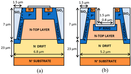
Figure 1.
Sketch of the proposed devices. (a) Planar gate semi superjunction (PSSJ). (b) Trench gate semi superjunction (TSSJ). Not to scale.
2. Benchmark Structures
To accurately evaluate the performance enhancements provided by the proposed tilted trench semi-superjunction designs, it is essential to establish benchmark structures for comparison. The benchmarks chosen for this study are a standard planar MOSFET and an ideal vertical SSJ MOSFET. The planar MOSFET serves as a primary benchmark structure due to its widespread use in power electronics and provides a reference for the performance of traditional SiC devices under similar conditions. The ideal vertical SSJ MOSFET represents the theoretical best-case scenario for trench etching and sidewall implantation SSJ devices, serving to benchmark the upper limits of performance achievable with this technology. The study of the ideal case allows an understanding of the maximum potential improvements possible with this SSJ approach and the determination of whether there is a sufficient margin to explore the more practical, yet non-ideal, tilted trench design. The benchmark structures are sketched in Figure 2.
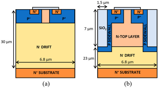
Figure 2.
Sketch of the reference devices. (a) Planar (benchmark). (b) Vertical semi-superjunction (ideal). Not to scale.
All simulated structures in this work utilize a 4H-SiC substrate, which is 100 µm thick and has a constant nitrogen doping concentration of 1 × 1019 cm−3. To achieve a BV greater than 3.3 kV, the devices have a drift region thickness of 30 µm with a constant doping concentration of 3 × 1015 cm−3. The n+ source region has a peak doping concentration of 1 × 1019 cm−3 and the p contact for the body region has a constant doping concentration of 1 × 1019 cm−3 to ensure good ohmic contact. More specifically, a Gaussian doping profile is assumed for the body and source regions, reflecting the realistic diffusion and implantation processes commonly used during device fabrication. In contrast, the epitaxial layer and substrate are modeled with constant doping concentrations. This approximation is widely adopted in device simulations due to the high uniformity typically achieved in epitaxial growth processes and the homogeneous nature of substrate materials. To capture the transition between the epitaxial layer and the substrate accurately, a Gaussian transition doping profile is applied at their interface, ensuring a smooth change in doping concentration and preserving the physical accuracy of the model. A 50 nm thick gate oxide is considered, with a fixed charge at the gate oxide/semiconductor interface of 2 × 1012 cm−3 [26,27]. The area factor is adjusted to consider a total area of the simulated devices of 1 cm2.
2.1. Planar MOSFET
A standard planar MOSFET (Figure 2a) was simulated with a cell pitch of 6.8 µm to maintain consistency with the other simulated structures. The threshold voltage (VTH) was around 4.5 V, as shown by the transfer characteristic in Figure 3a. A JFET width of 1.2 µm was considered, and a constant doping concentration of 6 × 1015 cm−3 was also included to improve the on-state conduction of the device [28]. The resulting output characteristic for a VGS of 18 V is reported in Figure 3b. The corresponding RDS-ON is 14.3 mΩ·cm2 [29]. The reverse characteristic is shown in Figure 3c, indicating a BV of 4000 V. The electric field (EF) distribution at 2 kV, reported in Figure 3d, shows that the electric field peak (1.7 MV/cm) is located at the bottom of the body region, while the gate oxide is free from EF pressure.
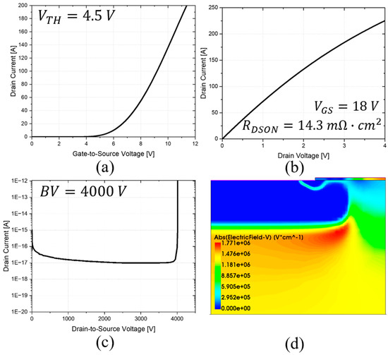
Figure 3.
Planar structure performance. (a) Transfer characteristic. (b) On-state characteristic. (c) Off-state characteristic. (d) Electric field distribution at 2 kV.
2.2. Vertical Semi-Superjunction MOSFET
To achieve a uniform electric field distribution in the superjunction designs, a charge balance between the n-layer and the p-type sidewall implantation should be attained [30] (see Equation (1)).
This balance can be obtained following the formula reported in Equation (2).
where ND and WN are the doping concentration and width of the n-layer, respectively, and NA and WP are the doping concentration and width of the p-type sidewall, respectively. According to Equation (2), the ideal semi-superjunction is achieved when the trench angle is 0 degrees, resulting in a constant WN along the trench and thus achieving a fully compensated charge between the p-type sidewall and the contiguous n-zone. This 0-degree trench configuration allows for the best performance with this design.
A vertical SSJ with trench etching and sidewall implantation was simulated as an ideal case. The design featured an oxide-filled trench 3 µm wide and 7 µm deep. A sidewall p-type implantation was considered to allow the SJ effect. The p-doping profiles along the sidewalls were modeled with Gaussian distributions to accurately reflect realistic implantation and diffusion processes. A fixed charge of 5 × 1012 cm−3 at the interface between the SJ trench and the semiconductor was considered [31] to take into consideration additional edge roughness. All other design parameters were consistent with those of the planar MOSFET. To ensure the charge balance, an n-top layer with a doping concentration (NTOP) higher than the drift region was considered next to the oxide trench.
An analysis of its performance was conducted by varying the p-sidewall peak doping concentration and implantation depth (dSW). Variations in the JFET n-top layer doping concentrations of 2 × 1016 cm−3 and 3 × 1016 cm−3, as well as p-sidewall depths of 200 nm to 400 nm, were considered. The resulting behavior of the BV is reported in Figure 4a.
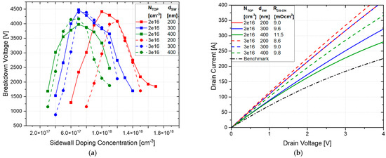
Figure 4.
Vertical SSJ performance. (a) Analysis of the breakdown voltage versus sidewall peak doping concentration, varying NTOP (solid line 2 × 1016 cm−3, dotted line 3 × 1016 cm−3) and sidewall depth (red 200 nm, blue 300 nm, green 400 nm) for the vertical SSJ. (b) On- state characteristics and RDS-ON, varying NTOP and sidewall depth for the vertical SSJ. The sidewall doping concentration is set to the values that provide the best charge balance for each combination of NTOP and dSW.
A wide implantation window was obtained for most of the design parameter combinations, improving the BV by up to 11.9% compared to the planar case.
A significant improvement in the on-state conduction was also achieved, with RDS-ON varying from 8.6 mΩ·cm2 to 11.5 mΩ·cm2, ensuring an improvement from 21.7% to 49.8%, as shown in Figure 4b. The on-state characteristics were simulated using the p-sidewall concentration that achieved the optimal charge balance for each combination of N-top layer doping and sidewall depth, according to Figure 4a. In Figure 5, the EF distribution at 2 kV is reported, showing reasonable values for the EF peak value.
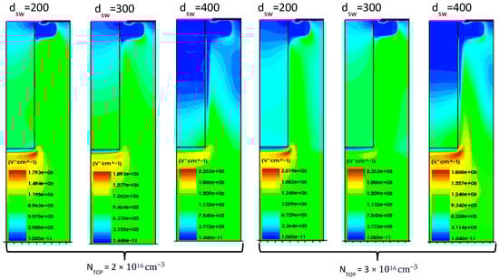
Figure 5.
Electric field distribution at 2 kV, varying NTOP and sidewall depth for the ideal vertical SSJ. The sidewall doping concentration corresponds to the optimal BV value for each case.
Despite significantly improved performance over the planar design, a 0-degree trench posed significant challenges for the implantation through the sidewalls. However, the promising results obtained from the ideal vertical SSJ case indicate that substantial performance enhancements are achievable through this technology. This suggests that there is a sufficient margin to explore the tilted trench design, which, although non-ideal, may offer a practical compromise between performance, fabrication feasibility, and cost.
2.3. Tilted Semi-Superjunction MOSFET
To overcome the challenges associated with implantation through a vertical sidewall and make the implantation process more feasible, a tilted trench with an angle of 10 degrees was considered, pivoting at the midpoint of the trench depth (i.e., 3.5 µm). This inclination facilitates the implantation process by providing better access to the trench sidewalls, reducing the difficulty of achieving uniform doping profiles. The details of the fabrication of SiC superjunction trenches have already been discussed by the authors in [32].
In an ideal vertical superjunction structure, the width of the n-type region (WN) would remain constant along the trench depth to ensure uniform charge compensation between the p- and n-type regions. In the tilted trench design, the trench wall slope causes a variation in WN along the trench depth, which affects the charge distribution. Specifically, when the n-top layer doping concentration is optimized to balance charges at the midpoint of the trench, this results in an overcompensation of positive charges (QP) above the pivot point and an overcompensation of negative charges (QN) below the pivot point. This uneven charge distribution can lead to localized electric field peaks, potentially increasing the risk of premature breakdown or affecting the device’s breakdown voltage.
The impact of this charge imbalance is further exacerbated at different depths of the trench. Above the pivot point, where QP is overcompensated, the electric field may be more concentrated, leading to higher field stress in these regions. Conversely, below the pivot point, the overcompensation of QN can create regions with a lower electric field intensity, which might reduce the overall effectiveness of the SJ effect. Therefore, while the tilted trench design simplifies fabrication, it necessitates the careful optimization of doping profiles and trench geometry to balance these competing effects and achieve the desired device performance.
An analysis of the performance of the proposed PSSJ and TSSJ designs is reported below.
Firstly, a planar channel semi-superjunction design with a tilted oxide trench (see Figure 1) is simulated, focusing on optimizing the SSJ effect while minimizing charge imbalance. To further exploit the SSJ effect, a TSSJ design is considered, incorporating a trench gate that is 0.8 µm wide and 1.5 µm deep. The absence of a JFET region in this design allows for a reduced cell pitch of 5.2 µm. Additionally, a p-ring with a high doping concentration of 5 × 1018 cm−3 is added at the bottom of the trench to shield the gate oxide from excessive electric fields, enhancing device reliability.
The analysis includes variations in sidewall doping concentration across different sidewall depths (200 nm, 300 nm, 400 nm) and different doping concentrations for the JFET n-top layer (2 × 1016 cm−3 and 3 × 1016 cm−3), aiming to optimize the overall device performance in terms of BV and RDS-ON. An overview of the doping concentrations and dimensions of the simulated structures is provided in Table 1.

Table 1.
Overview of the doping concentrations and dimensions of the simulated structures.
3. Results and Discussion
The performance of the proposed designs in terms of BV, EF distribution, and RDS-ON was evaluated through TCAD simulations. These simulations provide insights into how varying design parameters, such as doping concentrations and trench geometry, influence the electrical characteristics of planar and trench SSJ MOSFETs.
3.1. Planar Semi-Superjunction
The behavior of the BV as a function of the sidewall peak doping concentration is reported in Figure 6a. The maximum achievable BV is 4101 V, obtained with an n-top layer doping concentration of 2 × 1016 cm−3 and a sidewall doping concentration and depth of 9 × 1017 cm−3 and 300 nm, respectively. For a JFET n-layer doping concentration of 2 × 1016 cm−3, the BV across all sidewall depths approaches and indeed exceeds the benchmark value (4 kV) but remains below the ideal SSJ case (4.4 kV). This trend suggests that while the doping concentration is sufficient to establish a good electric field distribution, it does not fully optimize charge balancing. For a higher JFET n-top layer doping concentration (i.e., 3 × 1016 cm−3), the BV is significantly lower. This decrease can be attributed to an increased imbalance in the charge distribution between the n- and p-type regions, resulting in localized electric field enhancements that reduce the overall breakdown voltage.
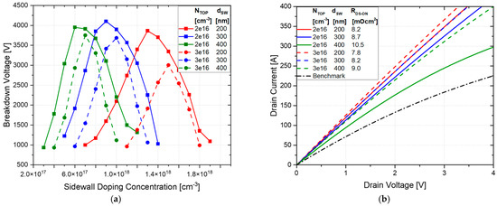
Figure 6.
PSSJ performance. (a) Analysis of the breakdown voltage versus the sidewall peak doping concentration with varying NTOP (solid line 2 × 1016 cm−3, dotted line 3 × 1016 cm−3) and sidewall depth (red 200 nm, blue 300 nm, green 400 nm) values for the PSSJ. (b) On-state characteristics and RDS-ON, varying NTOP and sidewall depth for the PSSJ. The sidewall doping concentration is set to the values that provide the best charge balance for each combination of NTOP and dSW.
Conversely, the lowest BV is observed for an n-top layer doping concentration of 3 × 1016 cm−3 with a sidewall depth of 200 nm as the high n-layer concentration and shallow p-sidewall result in maximum charge imbalance. This imbalance significantly reduces the effectiveness of charge compensation, leading to a BV of 3 kV.
Figure 6b shows the on-state characteristics and the relative RDS-ON values when varying the n-top layer doping concentration and sidewall depth. It is worth noting that the on-state performance is not significantly affected by the p-doped sidewall doping concentration. The RDS-ON decreases as the n-top layer doping concentration increases, whereas it increases when the sidewall depth decreases. This trend occurs because a higher doping concentration increases the number of charge carriers, reducing resistance, whereas a shallower sidewall enlarges the effective current conduction path, thereby reducing the overall resistance.
The best result is achieved with an n-top layer doping concentration of 3 × 1016 cm−3 and a sidewall depth of 200 nm, yielding an RDS-ON of 7.8 mΩ·cm2. This configuration provides an effective conduction path that minimizes resistance. Conversely, the least efficient result is observed for a constant n-top layer doping concentration of 2 × 1016 cm−3 with a sidewall depth of 400 nm, resulting in an RDS-ON of 10.5 mΩ·cm2. The deeper sidewall and lower doping concentration reduce the effective carrier density and cause a narrower conduction path, increasing resistance.
Figure 7 shows the electric field distribution at 2 kV for the optimal breakdown voltage corresponding to each combination of sidewall depth and n-top layer doping concentration. A deeper sidewall doping leads to a more uniform EF distribution along the oxide trench while also reducing the peak electric field. This uniformity is critical for enhancing device reliability, as it minimizes the likelihood of field-induced failures.
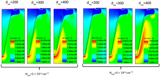
Figure 7.
Electric field distribution at 2 kV, varying the NTOP and sidewall depth for the PSSJ. The sidewall doping concentration corresponds to the optimal BV value for each case.
Table 2 reports an overview of the performance of this planar semi-superjunction design, including percentage variations relative to the benchmark planar structure. The optimal trade-off is observed in Case 2, with a BV of 4101 V and an RDS-ON of 8.7 mΩ·cm2, improving the performance of the benchmark by 2.5% and 48.7%, respectively.
Table 2.
Performance overview of the PSSJ and percentage variation relative to the benchmark.
3.2. Trench Semi-Superjunction
The BV versus the sidewall peak doping concentration for the trench gate semi-superjunction design is reported in Figure 8a. Similar trends to the planar structure are observed, but the reduced pitch in the trench design enables higher BV values across a broader range of design parameter combinations. More specifically, the benchmark values are exceeded for most parameter combinations. The best BV value occurs again at a doping concentration of 2 × 1016 cm−3 with a sidewall depth of 300 nm, resulting in a BV of 4206 V, which improves the value of the benchmark by 5.0%.
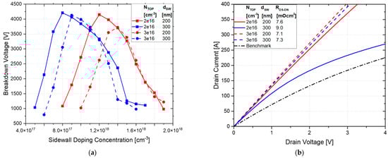
Figure 8.
TSSJ performance. (a) Analysis of the breakdown voltage versus sidewall peak doping concentration, varying NTOP (solid line 2 × 1016 cm−3, dotted line 3 × 1016 cm−3) and sidewall depth (red 200 nm, blue 300 nm, green 400 nm) for the vertical SSJ. (b) On-state characteristics and RDS-ON, varying NTOP and sidewall depth for the TSSJ. The sidewall doping concentration is set to the values that provide the best charge balance for each combination of NTOP and dSW.
The reduced pitch between the trenches further enhances electric field management, allowing for a higher BV. The reduction in SJ n-pillar width allows for better SJ charge balancing (towards the bottom of the SJ trench). The incorporation of a p-well below the gate trench shifts the EF peak away from the oxide, enhancing gate reliability and reducing the risk of oxide breakdown. As a result, the smaller cell pitch reduces the maximum EF compared to the PSSJ structure, further improving the electric field profile at 2 kV, as shown in Figure 9.
Figure 9.
Electric field distribution at 2 kV, varying NTOP and sidewall depth for the TSSJ. The sidewall doping concentration corresponds to the optimal BV value for each case.
The trench design also significantly enhances on-state conduction in certain cases, achieving much better performance compared to the standard planar and planar gate SSJ structures. Figure 8b presents the on-state characteristics and the corresponding RDS-ON. The lowest RDS-ON value is 7.1 mΩ·cm2 (67.3% lower than the benchmark), obtained with a doping concentration of the n-top layer of 3 × 1016 cm−3 and sidewall depth of 200 nm.
For lower n-top layer doping concentrations (e.g., 2 × 1016 cm−3), the depletion region becomes excessively large for deeper sidewall dopings, hindering current conduction between the gate trench and the deep SJ trenches. In other words, the current path between the p-sidewall and the p-ring area becomes very narrow, obstructing the current flow, as shown in Figure 10. This narrow path limits carrier mobility and increases resistance. Thus, optimizing the trench width and sidewall depth is crucial for balancing RDS-ON and BV. According to this, a sidewall doping depth of 400 nm is not considered for this design to prevent worsening conduction performance. The cell pitch is determined according to the resulting JFET resistance, ensuring that the trench dimensions support efficient conduction without compromising breakdown performance. A summary of the performance of the trench structure is provided in Table 3. The best trade-off for the trench gate design is obtained in Case 4, with a BV of 4127 V and an RDS-ON of 7.3 mΩ·cm2, improving the benchmark by 3.1% and 64.8%, respectively.
Figure 10.
Total current density path for an n-top layer doping concentration of 3 × 1016 cm−3 and (a) dSW = 200 nm; and (b) dSW = 400 nm. In the figure is highlighted the junction line (black lines).
Table 3.
Performance overview of the TSSJ and percentage variation relative to the benchmark.
3.3. The Graded Approach
As the width of the n-SJ layer near the trench varies due to the trench inclination, to perfectly balance the charge alongside the tilted trench, the n-top layer doping concentration should decrease as the n-width increases to maintain a constant charge density all across. This approach addresses the issue of unbalanced charges along the tilted trench by compensating for the varying widths of the n-region. In areas where the n-width is greater, the doping concentration is reduced to prevent excessive charge accumulation, while in narrower sections, the n-doping concentration is increased to ensure sufficient charge balance.
A simple and feasible approach to achieve this graded doping profile is to divide the n-top layer into several sections, each with a different doping concentration. This method is straightforward because different doping profiles can be easily achieved through multiple epitaxial growth steps at the initial drift epi growth stage, allowing for more precise control of the charge distribution between the p- and n-regions.
By tailoring the doping levels to the varying widths of the n-region, the graded approach can effectively balance the charge, enhancing the overall performance and reliability of the tilted trench SSJ design.
To explore the effectiveness of this graded approach, a simulation was performed on the PSSJ considering a sidewall depth of 300 nm and a peak p-doping concentration of 1 × 1018 cm−3, which were found to be the optimal parameters for the constant n-top layer case. The n-top layer was divided into four sections, with doping concentrations of 5.0 × 1016 cm−3, 2.5 × 1016 cm−3, 2.1 × 1016 cm−3, and 1.7 × 1016 cm−3. The resulting doping profile is reported in Figure 11.
Figure 11.
Graded n-top layer doping concentration.
The simulation showed a BV of 4055 V and an RDS-ON of 8.2 mΩ·cm2. Therefore, the BV remains high (>4 kV), and the graded approach results in a further 6% improvement in RDS-ON. An overview of the performance of all the analyzed designs is reported in Table 4. These results suggest that there is potential for further optimization by tuning the number of zones, their extension, and their doping concentration.
Table 4.
General performance overview and percentage variation relative to the benchmark.
However, the graded approach might not be suitable for trench designs due to the presence of the p-ring, an external element that further disturbs charge balance. The p-ring complicates the implementation of a precise doping gradient, as it introduces additional variability in the electric field and charge distribution. Consequently, while the graded approach shows promise for the PSSJ design, its applicability to trench-based designs may be limited.
4. Conclusions
This paper presents a detailed analysis of 3.3 kV SiC MOSFETs utilizing a tilted trench semi-superjunction design, demonstrating a cost-effective approach to improving device performance. Through TCAD simulations, we demonstrated the advantages of this design over conventional planar structures, showing an enhanced breakdown voltage and reduced on-state resistance. For the planar gate SSJ design, the best trade-off between on-state and blocking performance was achieved with a p-sidewall doping depth of 300 nm and a JFET n-top layer concentration of 2 × 1016 cm−3, resulting in improvements of 2.5% in the BV and 48.7% in the RDS-ON compared to the benchmark. In the trench gate SSJ design, the trade-off was further optimized, with improvements over the benchmark of 3.1% for BV and 64.8% for RDS-ON.
Additionally, the graded approach was explored by dividing the n-top layer into four zones, each with a different constant doping concentration. This method provided a further improvement of 6% in RDS-ON for the planar gate design without adding any significant fabrication complexity. These findings suggest that tilted trench SSJ designs offer a promising strategy for enhancing the performance and reliability of SiC MOSFETs, making them well suited for demanding power electronic applications.
Author Contributions
Conceptualization, M.B., K.M., A.B.R., P.M.G., V.K., V.A.S., L.M., A.I. and M.A.; methodology, M.B. and K.M.; software, M.B. and K.M.; validation, M.B., K.M., V.K. and L.M.; formal analysis, M.B., K.M. and M.A.; investigation, M.B., K.M., A.B.R. and M.A.; resources, V.A.S., P.M.G., A.I. and M.A.; data curation, M.B. and K.M.; writing—original draft preparation, M.B.; writing—review and editing, M.B. and M.A.; visualization, M.B.; supervision, M.A.; M.B. and K.M. equally contributed to this work. All authors have read and agreed to the published version of the manuscript.
Funding
This research received no external funding.
Data Availability Statement
The original contributions presented in the study are included in the article, further inquiries can be directed to the corresponding author.
Conflicts of Interest
The authors declare no conflicts of interest.
References
- Baliga, B.J. Silicon carbide power devices. In Springer Handbook of Semiconductor Devices; Springer International Publishing: Cham, Switzerland, 2022; pp. 491–523. [Google Scholar]
- Lorenz, L.; Deboy, G.; Zverev, I. Matched Pair of CoolMOS Transistor With SiC-Schottky Diode—Advantages in Application. IEEE Trans. Ind. Appl. 2004, 40, 1265–1272. [Google Scholar] [CrossRef]
- Mori, S.; Aketa, M.; Sakaguchi, T.; Nanen, Y.; Asahara, H.; Nakamura, T.; Kimoto, T. High-Temperature Characteristics of 3-kV 4H-SiC Reverse Blocking MOSFET for High-Performance Bidirectional Switch. IEEE Trans. Electron Devices 2017, 64, 4167–4174. [Google Scholar] [CrossRef]
- Boccarossa, M.; Maresca, L.; Borghese, A.; Riccio, M.; Breglio, G.; Irace, A.; Salvatore, G.A. Substantial Improvement of the Short-circuit Capability of a 1.2 kV SiC MOSFET by a HfO2/SiO2 Ferroelectric Gate Stack. In Proceedings of the 2024 36th International Symposium on Power Semiconductor Devices and ICs (ISPSD), Bremen, Germany, 2–6 June 2024; pp. 88–91. [Google Scholar] [CrossRef]
- Duan, Y.; Zhang, Y.-L.; Zhang, J.Q.; Liu, P. Development of SiC Superjunction MOSFET: A Review. In Proceedings of the 2022 19th China International Forum on Solid State Lighting & 2022 8th International Forum on Wide Bandgap Semiconductors (SSLCHINA: IFWS), Suzhou, China, 7–10 February 2023; pp. 13–17. [Google Scholar] [CrossRef]
- Masuda, T.; Saito, Y.; Kumazawa, T.; Hatayama, T.; Harada, S. 0.63 mΩcm2/1170 V 4H-SiC Super Junction V-Groove Trench MOSFET. In Proceedings of the 2018 IEEE International Electron Devices Meeting (IEDM), San Francisco, CA, USA, 1–5 December 2018; pp. 8.1.1–8.1.4. [Google Scholar] [CrossRef]
- Udrea, F.; Deboy, G.; Fujihira, T. Superjunction Power Devices, History, Development, and Future Prospects. IEEE Trans. Electron Devices 2017, 64, 713–727. [Google Scholar] [CrossRef]
- Baba, M.; Tawara, T.; Morimoto, T.; Harada, S.; Takei, M.; Kimura, H. Ultra-Low Specific on-Resistance Achieved in 3.3 kV-Class SiC Superjunction MOSFET. In Proceedings of the 2021 33rd International Symposium on Power Semiconductor Devices and ICs (ISPSD), Nagoya, Japan, 30 May 2021–3 June 2021; pp. 83–86. [Google Scholar] [CrossRef]
- Kosugi, R.; Sakuma, Y.; Kojima, K.; Itoh, S.; Nagata, A.; Yatsuo, T.; Tanaka, Y.; Okumura, H. First experimental demonstration of SiC super-junction (SJ) structure by multi-epitaxial growth method. In Proceedings of the 2014 IEEE 26th International Symposium on Power Semiconductor Devices & IC’s (ISPSD), Waikoloa, HI, USA, 15–19 June 2014; pp. 346–349. [Google Scholar] [CrossRef]
- Harada, S.; Kobayashi, Y.; Kyogoku, S.; Morimoto, T.; Tanaka, T.; Takei, M.; Okumura, H. First Demonstration of Dynamic Characteristics for SiC Superjunction MOSFET Realized using Multi-epitaxial Growth Method. In Proceedings of the 2018 IEEE International Electron Devices Meeting (IEDM), San Francisco, CA, USA, 1–5 December 2018; pp. 8.2.1–8.2.4. [Google Scholar] [CrossRef]
- Kosugi, R.; Ji, S.; Mochizuki, K.; Kouketsu, H.; Kawada, Y.; Fujisawa, H.; Kojima, K.; Yonezawa, Y.; Okumura, H. Strong impact of slight trench direction misalignment from [112¯0] on deep trench filling epitaxy for SiC super-junction devices. Jpn. J. Appl. Phys. 2017, 56, 04CR05. [Google Scholar] [CrossRef]
- Saito, W.; Omura, I.; Aida, S.; Koduki, S.; Izumisawa, M.; Ogura, T. Semisuperjunction MOSFETs: New design concept for lower on-resistance and softer reverse-recovery body diode. IEEE Trans. Electron Devices 2003, 50, 1801–1806. [Google Scholar] [CrossRef]
- Saito, W.; Omura, I.; Aida, S.; Koduki, S.; Izumisawa, M.; Yoshioka, H.; Ogura, T. High Breakdown Voltage (≫1000 V) Semi-Superjunction MOSFETs Using 600-V Class Superjunction MOSFET Process. IEEE Trans. Electron Devices 2005, 52, 2317–2322. [Google Scholar] [CrossRef]
- Saito, I.O.W. Over 1000V Semi-Superjunction MOSFET with Ultra-Low On-Resistance blow the Si-Limit. In Proceedings of the ISPSD ’05. The 17th International Symposium on Power Semiconductor Devices and ICs, Santa Barbara, CA, USA, 23–26 May 2005; pp. 27–30. [Google Scholar] [CrossRef]
- Kosugi, R.; Ji, S.; Mochizuki, K.; Adachi, K.; Segawa, S.; Kawada, Y.; Yonezawa, Y.; Okumura, H. Breaking the Theoretical Limit of 6.5 kV-Class 4H-SiC Super-Junction (SJ) MOSFETs by Trench-Filling Epitaxial Growth. In Proceedings of the 2019 31st International Symposium on Power Semiconductor Devices and ICs (ISPSD), Shanghai, China, 19–23 May 2019; pp. 39–42. [Google Scholar] [CrossRef]
- Melnyk, K.; Renz, A.B.; Cao, Q.; Gammon, P.M.; Lophitis, N.; Maresca, L.; Irace, A.; Nistor, I.; Rahimo, M.; Antoniou, M. 3.3 kV 4H-SiC Trench Semi-Superjunction Schottky Diode With Improved ON-State Resistance. IEEE Trans. Electron Devices 2024, 71, 5573–5580. [Google Scholar] [CrossRef]
- Melnyk, K.; Renz, A.B.; Cao, Q.; Gammon, P.M.; Shah, V.A.; Lophitis, N.; Rahimo, M.; Nistor, I.; Scognamillo, C.; Borghese, A.; et al. Design and Optimization of 3.3 kV Silicon Carbide Semi-Superjunction Schottky Power Devices. In Proceedings of the 2024 36th International Symposium on Power Semiconductor Devices and ICs (ISPSD), Bremen, Germany, 2–6 June 2024; pp. 132–135. [Google Scholar] [CrossRef]
- Baker, G.W.C.; Gammon, P.M.; Renz, A.B.; Vavasour, O.; Chan, C.W.; Qi, Y.; Dai, T.; Li, F.; Zhang, L.; Kotagama, V.; et al. Optimization of 1700-V 4H-SiC Semi-Superjunction Schottky Rectifiers with Implanted P-Pillars for Practical Realization. IEEE Trans. Electron Devices 2022, 69, 1924–1930. [Google Scholar] [CrossRef]
- Melnyk, K.; Boccarossa, M.; Renz, A.B.; Cao, Q.; Gammon, P.M.; Antoniou, M. Cost-Effective Design and Optimization of a 3300-V Semi-Superjunction 4H-SiC MOSFET Device. In Proceedings of the International Conference on Silicon Carbide and Related Materials (ICSCRM), Raleigh, NC, USA, 29 September–4 October 2024. [Google Scholar]
- Synopsys Sentaurus, Sentaurus Device User Guide Version V-2023.12, December 2023. Available online: https://solvnet.synopsys.com/Install/installation_guide.jsp?id=226&releasedate=2023-12-04 (accessed on 22 December 2024).
- Lee, S.; Chen, F.; Sarlioglu, B. Universally Applicable DC-Link RC Snubber Design Method for Switching Voltage Overshoot Reduction. IEEE Trans. Ind. Electron. 2025, 72, 1249–1260. [Google Scholar] [CrossRef]
- Xu, M.; Yang, X.; Li, J. C-RC Snubber Optimization Design for Improving Switching Characteristics of SiC MOSFET. IEEE Trans. Power Electron. 2022, 37, 12005–12016. [Google Scholar] [CrossRef]
- Baker, G.W.C.; Chan, C.; Renz, A.B.; Qi, Y.; Dai, T.; Li, F.; Shah, V.A.; Mawby, P.A.; Antoniou, M.; Gammon, P.M. Optimization of 1700-V 4H-SiC Superjunction Schottky Rectifiers With Implanted P-Pillars for Practical Realization. IEEE Trans. Electron Devices 2021, 68, 3497–3504. [Google Scholar] [CrossRef]
- Zarȩbski, J.; Górecki, K. Modelling CoolMOS transistors in SPICE. IEE Proc.-Circuits Devices Syst. 2006, 153, 46–52. [Google Scholar] [CrossRef]
- Górecki, K.; Zarębski, J. Modelling CoolMOSC3 transistor characteristics in SPICE. Int. J. Numer. Model. Electron. Netw. Devices Fields 2010, 23, 127–139. [Google Scholar] [CrossRef]
- Yu, S.; White, M.H.; Agarwal, A.K. Experimental Determination of Interface Trap Density and Fixed Positive Oxide Charge in Commercial 4H-SiC Power MOSFETs. IEEE Access 2021, 9, 149118–149124. [Google Scholar] [CrossRef]
- Tachiki, K.; Kimoto, T. Improvement of Both n- and p-Channel Mobilities in 4H-SiC MOSFETs by High-Temperature N2 Annealing. IEEE Trans. Electron Devices 2021, 68, 638–644. [Google Scholar] [CrossRef]
- KNaydenov, K.; Donato, N.; Udrea, F.; Mihaila, A.; Romano, G.; Wirths, S.; Knoll, L. Clamped and Unclamped Inductive Switching of 3.3 kV 4H-SiC MOSFETs with 3D Cellular Layouts. Mater. Sci. Forum 2022, 1062, 627–631. [Google Scholar] [CrossRef]
- Kono, H.; Iguchi, T.; Hirakawa, T.; Irifune, H.; Kawano, T.; Furukawa, M.; Sano, K.; Yamaguchi, M.; Suzuki, H.; Tchouangue, G. 3.3 kV All SiC MOSFET Module with Schottky Barrier Diode Embedded SiC MOSFET. In Proceedings of the International Exhibition and Conference for Power Electronics, Intelligent Motion, Renewable Energy and Energy Management, Online, 3–7 May 2021. [Google Scholar]
- Saito, W. Theoretical limits of superjunction considering with charge imbalance margin. In Proceedings of the 2015 IEEE 27th International Symposium on Power Semiconductor Devices & IC’s (ISPSD), Hong Kong, China, 10–14 May 2015; pp. 125–128. [Google Scholar] [CrossRef]
- Matsushima, H.; Yamada, R.; Shima, A. Two Mechanisms of Charge Accumulation in Edge Termination of 4H-SiC Diodes Caused by High-Temperature Bias Stress and High-Temperature and High-Humidity Bias Stress. IEEE Trans. Electron Devices 2018, 65, 3318–3325. [Google Scholar] [CrossRef]
- Cao, Q.; Renz, A.B.; Gammon, P.M.; Lophitis, N.; Melnyk, K.; Antoniou, M. Trench Etch Processing for SiC Superjunction Schottky Diodes. In Proceedings of the International Conference on Silicon Carbide and Related Materials (ICSCRM), Raleigh, NC, USA, 29 September–4 October 2024. [Google Scholar]
Disclaimer/Publisher’s Note: The statements, opinions and data contained in all publications are solely those of the individual author(s) and contributor(s) and not of MDPI and/or the editor(s). MDPI and/or the editor(s) disclaim responsibility for any injury to people or property resulting from any ideas, methods, instructions or products referred to in the content. |
© 2025 by the authors. Licensee MDPI, Basel, Switzerland. This article is an open access article distributed under the terms and conditions of the Creative Commons Attribution (CC BY) license (https://creativecommons.org/licenses/by/4.0/).