Post-Bonding Crack-Induced Di-Cantilever Bending (PBC-DCB): A Novel Method for Quantitative Evaluation of Bonding Strength for Wafer-to-Wafer and Die-to-Wafer Hybrid Bonding
Abstract
1. Introduction
2. Experimental Method and Theoretical Model
2.1. Experimental Methods and Sample Preparation
2.2. PBC-DCB Model
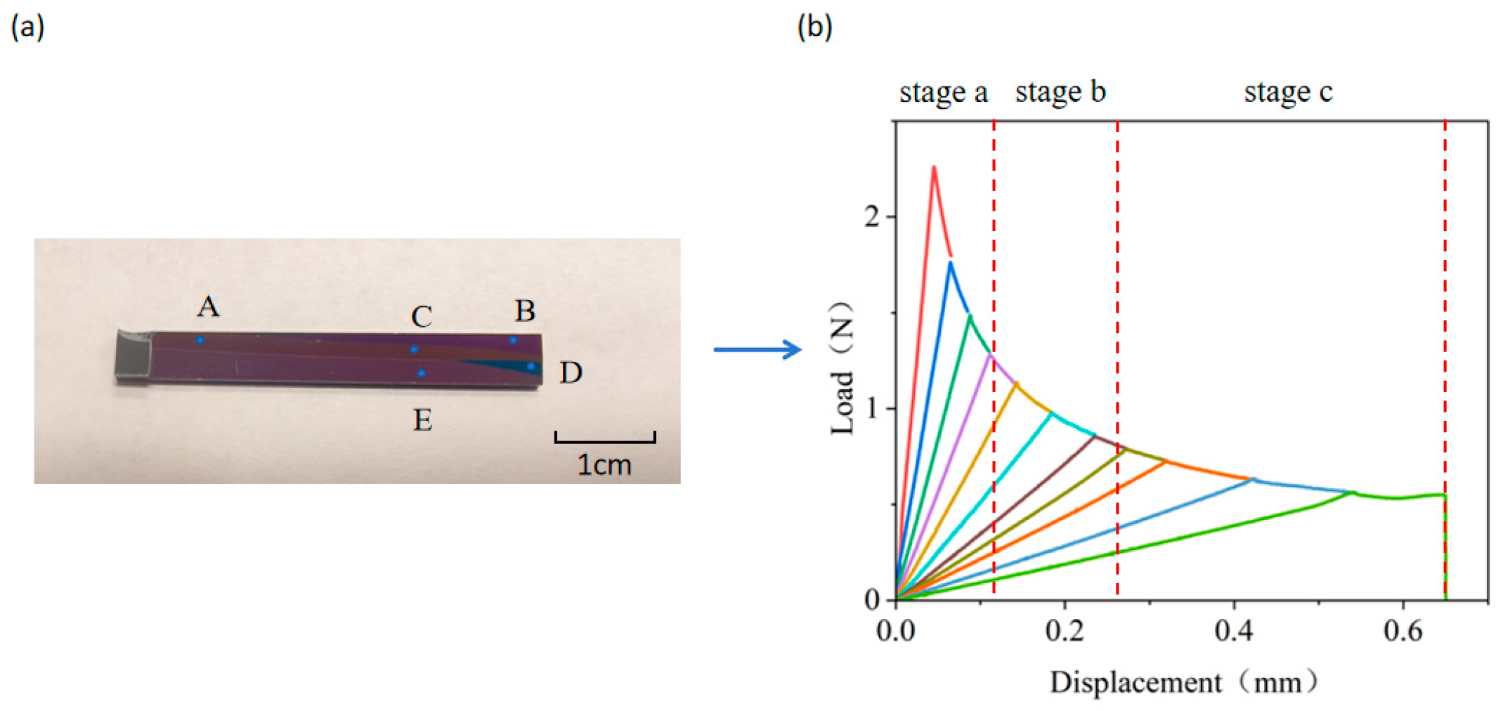
2.3. Crack Propagation Process of PBC-DCB
3. Experimental Results and Discussion
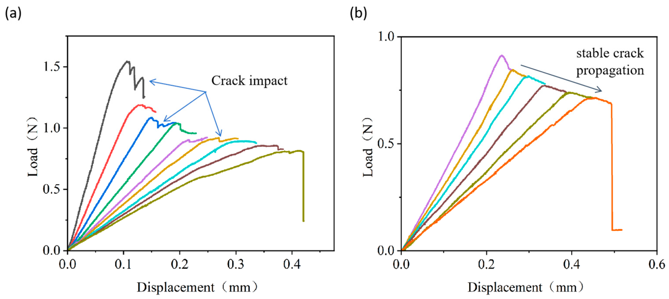
3.1. Load–Displacement Behavior of PBC-DCB
3.2. Load–Displacement Curve Differences of Pre- vs. Post-Bonding Crack Methods
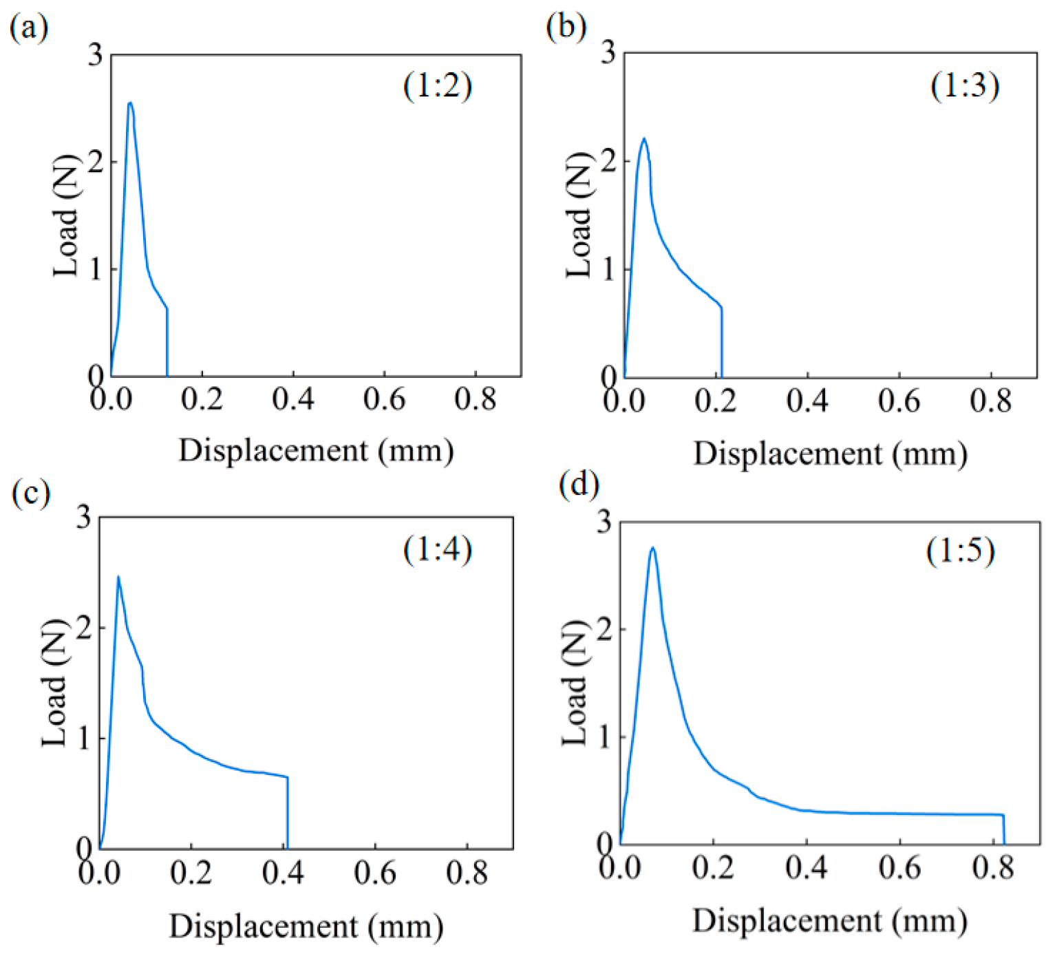
3.3. Impact of Pull Ring/Sample Length Ratios
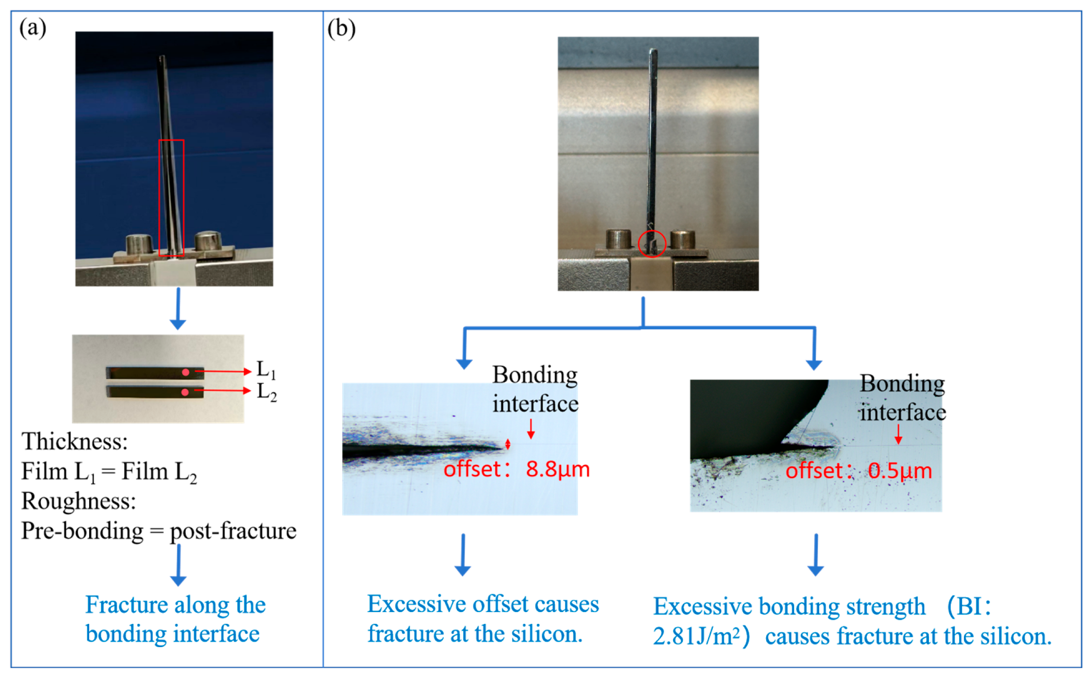
3.4. Fracture Interface Characterization
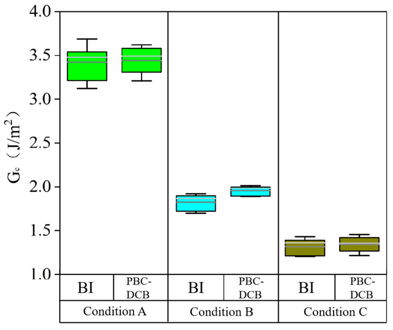
3.5. Comparison of the Bonding Strength Measurement Results Between BI and PBC-DCB
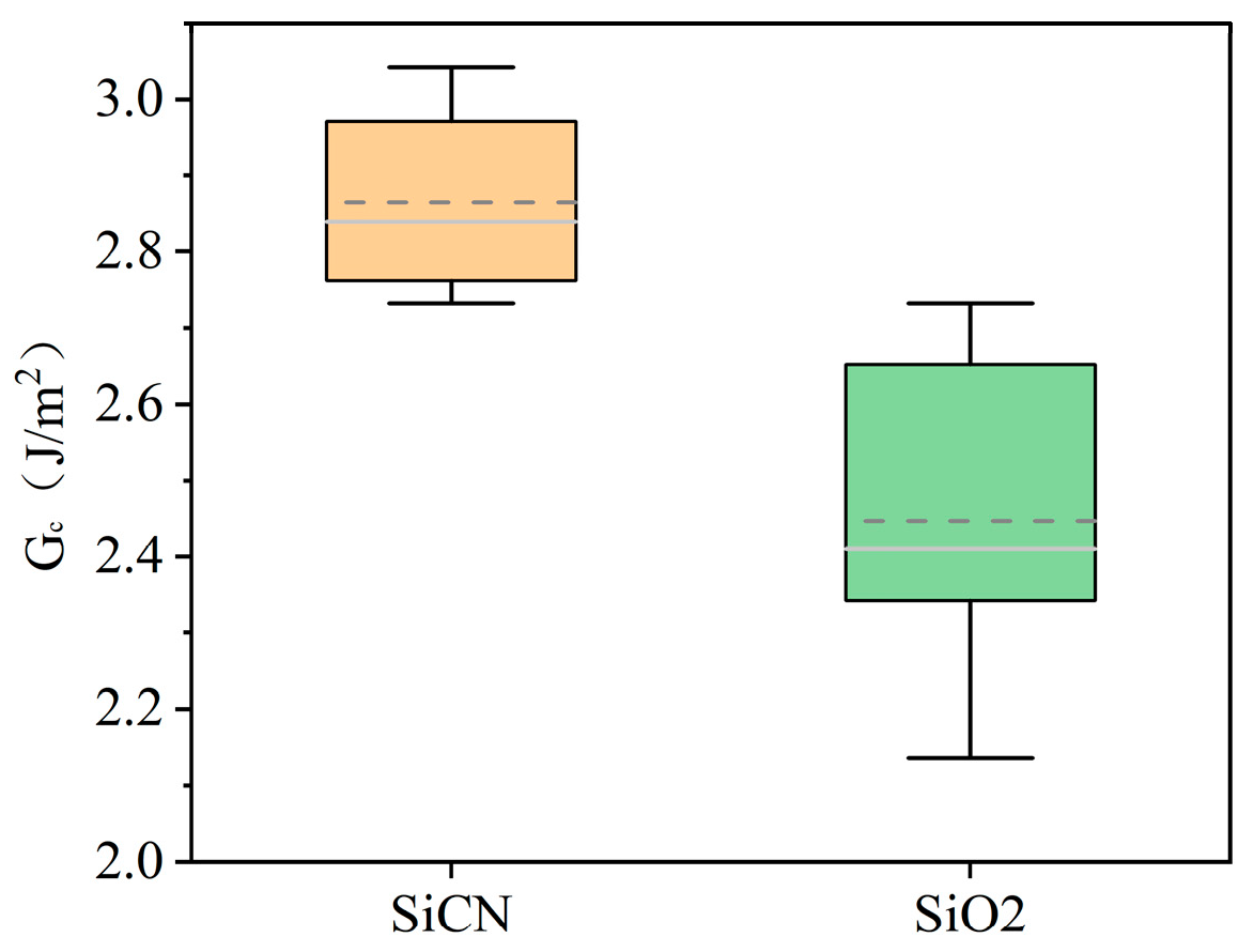
3.6. Comparison of the Bonding Strength Between SiCN and SiO2 Under the Same Conditions
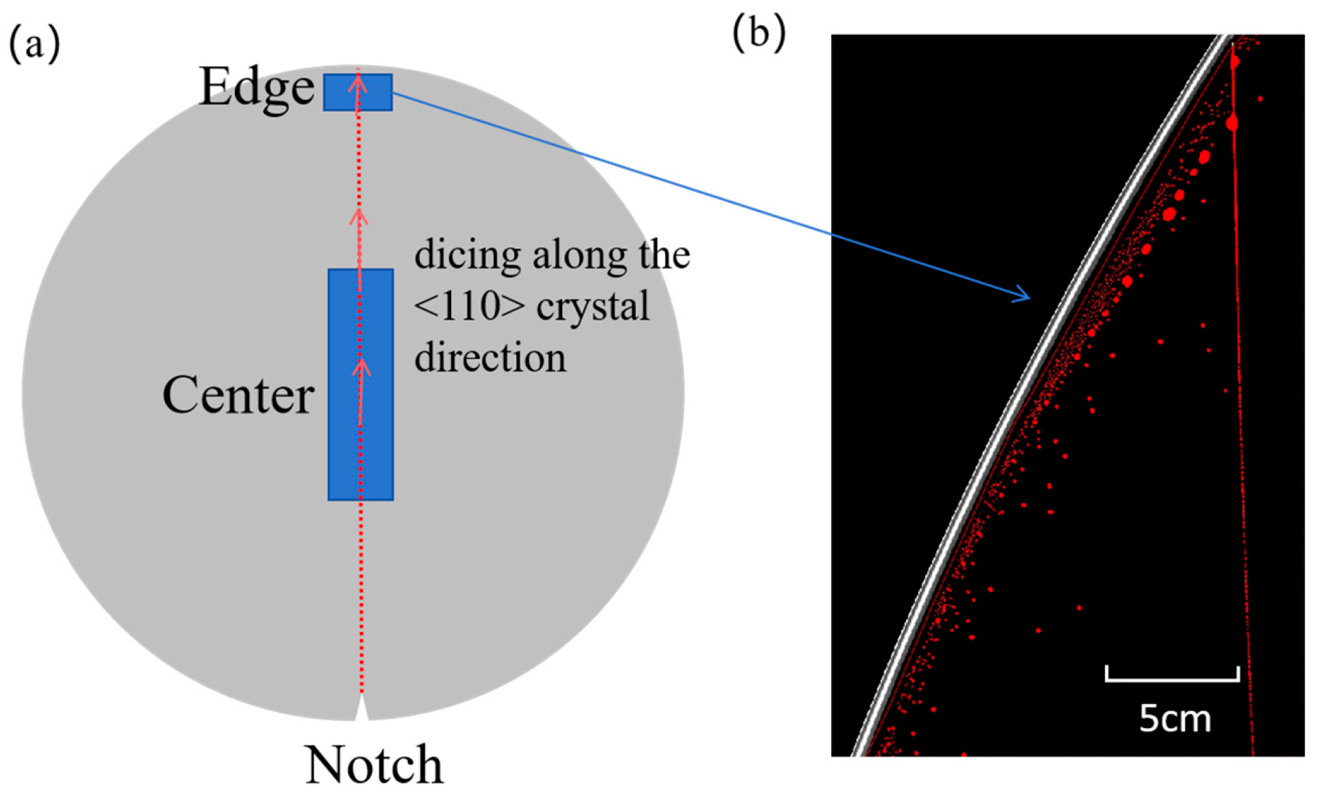
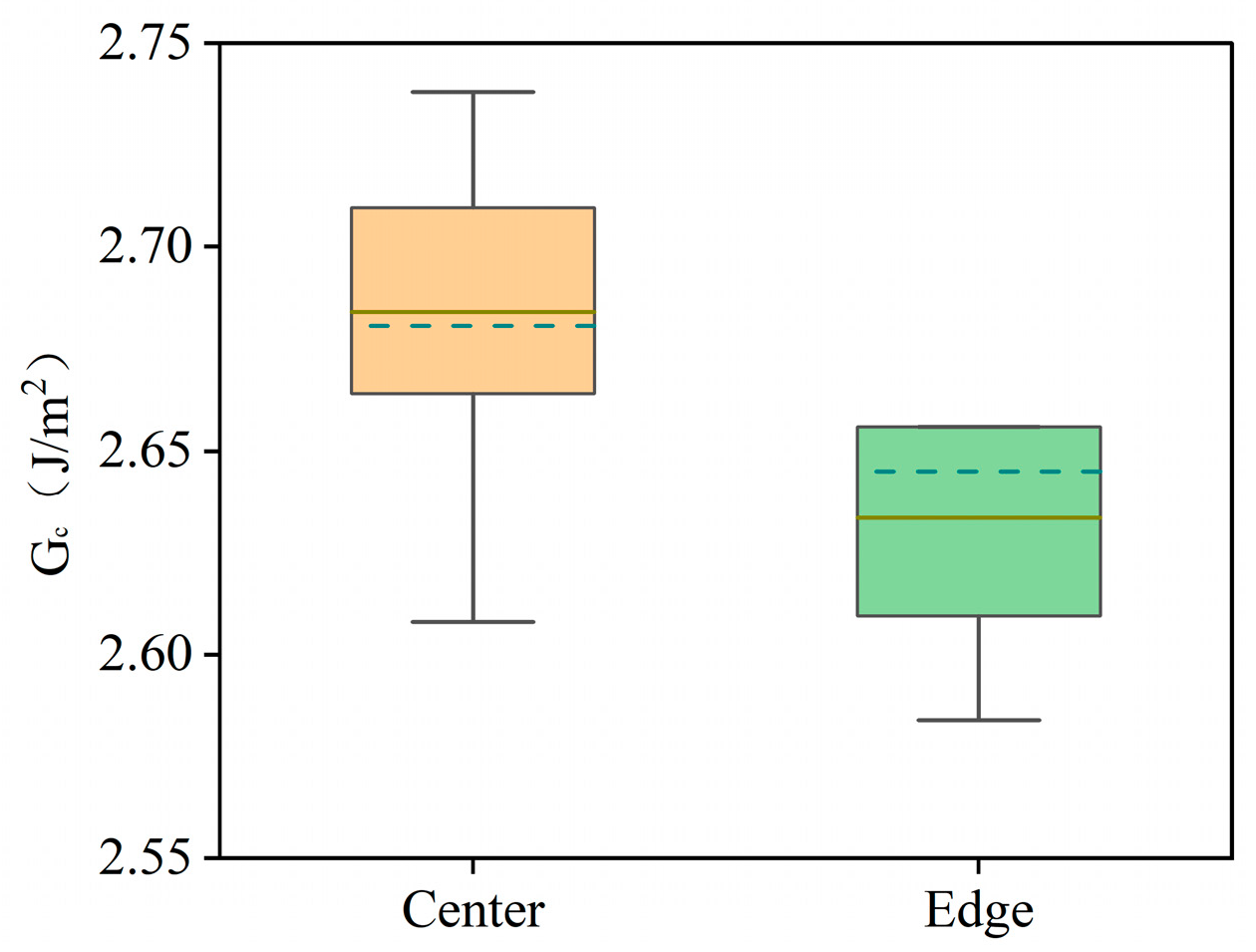
3.7. Measurement Results of Bonding Strength in Different Regions of Wafer Bonding
4. Conclusions
- (1)
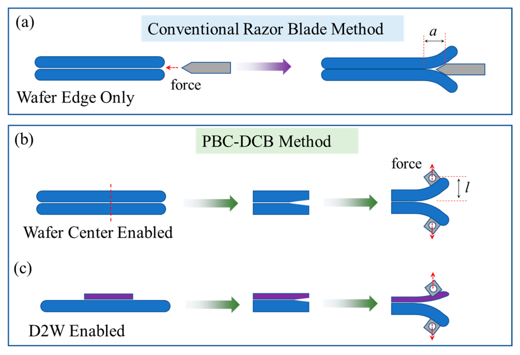
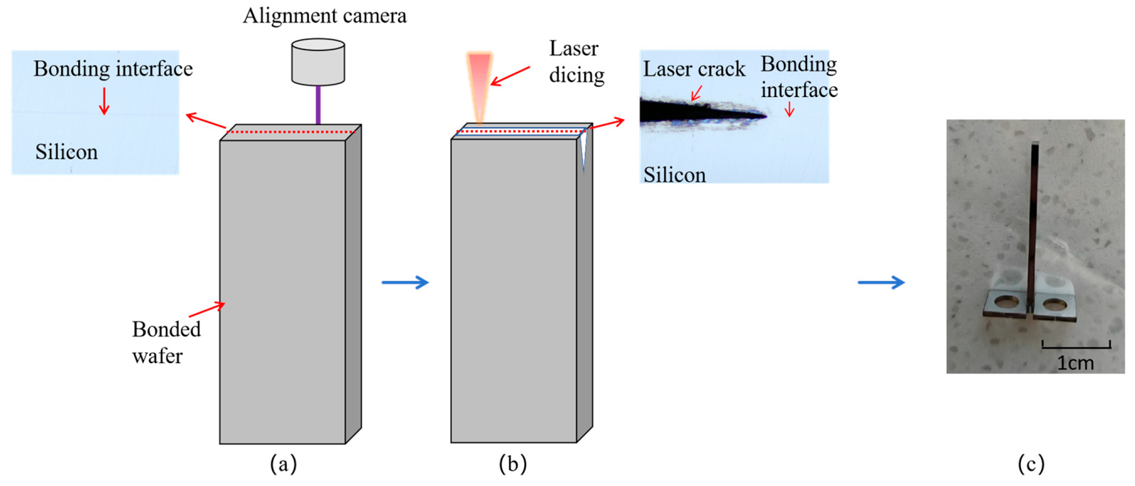
- The core contribution of PBC-DCB lies in its ability to overcome the inherent drawbacks of BI. Specifically, it enables bonding strength measurement at any location on the wafer—including the center region—and is fully applicable to D2W samples that lack bevel structures. Notably, the method’s innovative post-bonding laser crack strategy eliminates contamination and surface damage caused by pre-bonding processing, thereby ensuring the integrity of the bonding interface. This design fundamentally resolves the critical issue, where BI fails to reflect the overall bonding uniformity of wafers.
- (2)
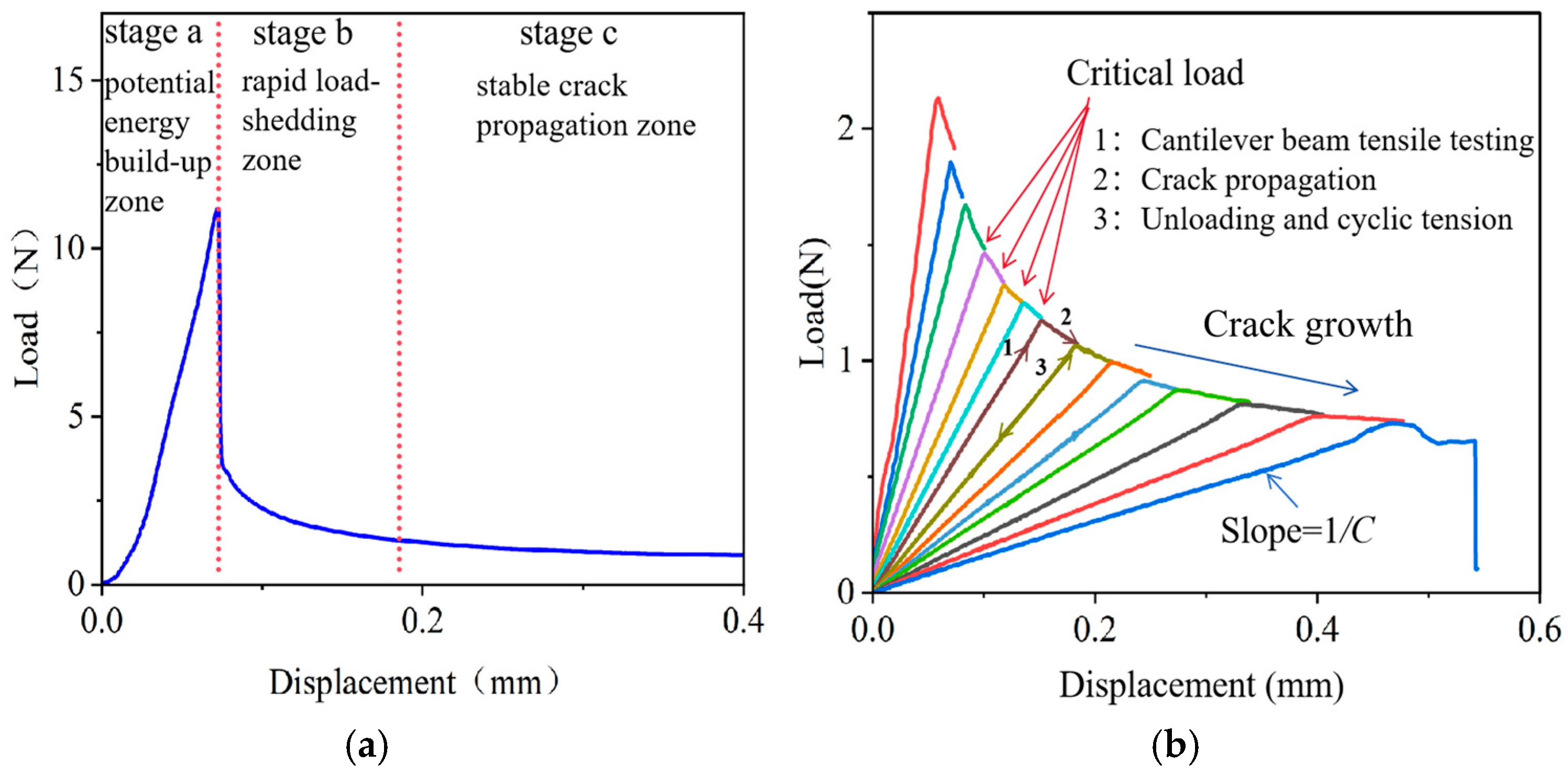
- Experimental validation further confirms the reliability of PBC-DCB: its measurements are highly consistent with those of BI, showing minimal deviation and significantly better repeatability. Additionally, parameter optimization enhances the test accuracy—with an optimal pull ring-to-sample length ratio, the load–displacement curve exhibits a stable descending segment, providing sufficient valid data for precise bonding strength calculation. Furthermore, fracture interface characterization validates that PBC-DCB accurately captures interfacial fracture behavior, avoiding misjudgments caused by improper crack positioning.
- (3)
- Regarding application potential: PBC-DCB can effectively distinguish differences in bonding performance between various dielectric materials, as well as between the center and edge regions of a wafer. Such a capability provides critical technical support for material selection, process optimization, and yield improvement in hybrid bonding—especially in high-density heterogeneous integration scenarios, such as AI chips. Overall, as a reliable testing tool, PBC-DCB holds broad prospects for application in both industrial production quality control and scientific research on hybrid bonding technology.
Supplementary Materials
Author Contributions
Funding
Data Availability Statement
Conflicts of Interest
References
- Bang, J.; Choi, Y.; Kim, M.; Kim, Y.; Rhu, M. vTrain: A Simulation Framework for Evaluating Cost-Effective and Compute-Optimal Large Language Model Training. In Proceedings of the 2024 57th IEEE/ACM International Symposium on Microarchitecture, Toronto, ON, Canada, 2–6 November 2024; pp. 153–167. [Google Scholar]
- Choi, K.S.; Kim, S.H.; Seo, J.W.; Kang, H.S.; Chu, S.W.; Bae, S.W.; Kwon, J.H.; Kim, G.S.; Park, Y.T.; Kwak, J.H.; et al. A Three Dimensional DRAM (3D DRAM) Technology for the Next Decades. In Proceedings of the 2024 IEEE Symposium on VLSI Technology and Circuits, Honolulu, HI, USA, 16–20 June 2024; pp. 1–2. [Google Scholar]
- Bai, F.; Jiang, X.; Wang, S.; Yu, B.; Tan, J.; Zuo, F.; Wang, C.; Wang, F.; Long, X.; Yu, G.; et al. A Stacked Embedded DRAM Array for LPDDR4/4X using Hybrid Bonding 3D Integration with 34GB/s/1Gb 0.88pJ/b Logic-to-Memory Interface. In Proceedings of the 2020 IEEE International Electron Devices Meeting, San Francisco, CA, USA, 12–18 December 2020; pp. 6.6.1–6.6.4. [Google Scholar] [CrossRef]
- Gholami, A.; Yao, Z.; Kim, S.; Hooper, C.; Mahoney, M.W.; Keutzer, K. AI and Memory Wall. IEEE Micro 2024, 44, 33–39. [Google Scholar] [CrossRef]
- Hsiung, C.K.; Chen, K.N. A Review on Hybrid Bonding Interconnection and Its Characterization. IEEE Nanotechnol. Mag. 2024, 18, 41–50. [Google Scholar] [CrossRef]
- Ji, H.-M.; Ji, L.; Che, F.-X.; Li, H.-Y.; Chui, K.-J.; Kawano, M. Wafer Level High Density Hybrid Bonding for High Performance Computing. In Proceedings of the 2020 IEEE International Symposium on the Physical and Failure Analysis of Integrated Circuits, Singapore, 20–23 July 2020; pp. 1–5. [Google Scholar] [CrossRef]
- Kim, J.; Zhu, L.; Torun, H.M.; Swaminathan, M.; Lim, S.K. Micro-bumping, Hybrid Bonding, or Monolithic? A PPA Study for Heterogeneous 3D IC Options. In Proceedings of the 2021 58th ACM/IEEE Design Automation Conference, San Francisco, CA, USA, 5–9 December 2021; pp. 1189–1194. [Google Scholar]
- Lannon, J.M.; Gregory, C.; Lueck, M.; Reed, J.D.; Huffman, C.A.; Temple, D. High Density Metal–Metal Interconnect Bonding for 3-D Integration. IEEE Trans. Compon. Packag. Manuf. Technol. 2012, 2, 71–78. [Google Scholar] [CrossRef]
- Sakuma, K.; Yu, R.; Polomoff, N.; Darling, L.; Chowdhury, P.; Raghavan, S.; Seifert, K.; Knickerbocker, J.; McHerron, D.; Li, M.; et al. Voids-free Die-level Cu/ILD Hybrid bonding. In Proceedings of the 2023 IEEE 73rd Electronic Components and Technology Conference, Las Vegas, NV, USA, 30 May–2 June 2023; pp. 800–805. [Google Scholar]
- Mehta, G.; Abdilla, J.; Hung, R.; Bazizi, E.M.; Bum, Y.C.; Bikajlevic, D.; Jiang, L.; Costrini, G. D2W Hybrid Bonding Challenges for HBM. In Proceedings of the 2024 IEEE International Memory Workshop, Monterey, CA, USA, 12–15 May 2024; pp. 1–4. [Google Scholar] [CrossRef]
- Nigussie, T.; Pan, T.H.; Lipa, S.; Pitts, W.S.; DeLaCruz, J.; Franzon, P. Design Benefits of Hybrid Bonding for 3D Integration. In Proceedings of the 2021 IEEE 71st Electronic Components and Technology Conference, San Diego, CA, USA, 1 June–4 July 2021; pp. 1876–1881. [Google Scholar]
- Vallin, Ö.; Jonsson, K.; Lindberg, U. Adhesion quantification methods for wafer bonding. Mater. Sci. Eng. R Rep. 2005, 50, 109–165. [Google Scholar] [CrossRef]
- Shao, S.; Niu, Y.; Wang, J.; Park, S.; Lee, B. Accessible determination of die-to-wafer bond strength with the Schwickerath test. Eng. Fract. Mech. 2020, 229, 106929. [Google Scholar] [CrossRef]
- Kim, Y.-S.; Nguyen, T.H.; Choa, S.-H. Enhancement of the Bond Strength and Reduction of Wafer Edge Voids in Hybrid Bonding. Micromachines 2022, 13, 537. [Google Scholar] [CrossRef] [PubMed]
- Dai, X.; Brillhart, M.V.; Ho, P.S. Adhesion measurement for electronic packaging applications using double cantilever beam method. IEEE Trans. Compon. Packag. Technol. 2000, 23, 101–116. [Google Scholar] [CrossRef]
- Kanninen, M.F. An augmented double cantilever beam model for studying crack propagation and arrest. Int. J. Fract. 1973, 9, 83–92. [Google Scholar] [CrossRef]
- Fuse, J.; Yoshihara, Y.; Sano, M.; Inoue, F. Bond Strength Measurement for Wafer-Level and Chip-Level Hybrid Bonding. In Proceedings of the 2024 IEEE 10th Electronics System-Integration Technology Conference, Prague, Czech Republic, 11–13 September 2024; pp. 1–5. [Google Scholar] [CrossRef]
- Lianto, P.; Raphael, R.E.; Tan, A.; Chia, C.K.; Li, X.; Lee, H.M.; Chen, X. SiCN CMP Integration for Hybrid Bonding Application. In Proceedings of the 2025 IEEE 75th Electronic Components and Technology Conference, San Diego, CA, USA, 27–30 May 2025; pp. 347–350. [Google Scholar]
- Ebiko, S.; Iacovo, S.; Chew, S.A.; Zhang, B.; Uedono, A.; Inoue, F. Exploring Bonding Mechanism of SiCN for Hybrid Bonding. In Proceedings of the 2024 IEEE 74th Electronic Components and Technology Conference, Orlando, FL, USA, 28–31 May 2024; pp. 1953–1957. [Google Scholar]
- Hahn, S.H.; Kim, W.; Shin, D.; Lee, Y.; Kim, S.; Choi, W.; Lim, K.; Moon, B.; Rhee, M. Contamination-Free Cu/SiCN Hybrid Bonding Process Development for Sub- μm Pitch Devices with Enhanced Bonding Characteristics. In Proceedings of the 2023 IEEE 73rd Electronic Components and Technology Conference, Las Vegas, NV, USA, 30 May–2 June 2023; pp. 1390–1396. [Google Scholar]
- Ma, K.; Bekiaris, N.; Hsu, C.H.; Xue, L.; Ramaswami, S.; Ding, T.; Probst, G.; Wernicke, T.; Uhrmann, T.; Wimplinger, M. 0.5 μm Pitch Wafer-to-wafer Hybrid Bonding at Low Temperatures with SiCN Bond Layer. In Proceedings of the 2024 IEEE 74th Electronic Components and Technology Conference, Orlando, FL, USA, 28–31 May 2024; pp. 331–336. [Google Scholar]
- Ma, K.; Bekiaris, N.; Ramaswami, S.; Ding, T.; Probst, G.; Burggraf, J.; Uhrmann, T. 0.5 ¼m Pitch Wafer-to-wafer Hybrid Bonding with SiCN Bonding Interface for Advanced Memory. In Proceedings of the 2023 IEEE 73rd Electronic Components and Technology Conference, Las Vegas, NV, USA, 30 May–2 June 2023; pp. 1110–1114. [Google Scholar]



| HF/W | Spacing | Pressure/Torr | NH3 Flow Rate/Sccm | N2 Flow Rate/Sccm | TMS Flow Rate/Sccm |
|---|---|---|---|---|---|
| 650 | 290 | 3.7 | 725 | 1200 | 350 |
| Parameter | Symbol (Unit) | Value |
|---|---|---|
| Young’s modulus of Si | Es (GPa) | 169 (<110>) |
| 128 (<100>) | ||
| Poisson’s ratio of Si | vs | 0.064 (<110>) |
| 0.28 (<100>) | ||
| Young’s modulus of SiCN | E0 (GPa) | 200 |
| Poisson’s ratio of SiCN | V0 | 0.21 |
| The thickness of Si-1 | h (μm) | 775 |
| The thickness of Si-2 | h (μm) | 775 |
| The thickness of SiCN/SiO2-1 | t (nm) | 200/300 |
| The thickness of SiCN/SiO2-2 | t (nm) | 200/300 |
| The width of the wafer | b (mm) | 4~5 |
| Half-length of nut | d (mm) | 0.60~0.65 |
Disclaimer/Publisher’s Note: The statements, opinions and data contained in all publications are solely those of the individual author(s) and contributor(s) and not of MDPI and/or the editor(s). MDPI and/or the editor(s) disclaim responsibility for any injury to people or property resulting from any ideas, methods, instructions or products referred to in the content. |
© 2025 by the authors. Licensee MDPI, Basel, Switzerland. This article is an open access article distributed under the terms and conditions of the Creative Commons Attribution (CC BY) license (https://creativecommons.org/licenses/by/4.0/).
Share and Cite
Zheng, T.; Xu, Y.; Mei, C.; Chen, Y.; Chang, L.; Yang, G.; Hu, Q.; Shi, T.; Yuan, Y.; Yu, Z.; et al. Post-Bonding Crack-Induced Di-Cantilever Bending (PBC-DCB): A Novel Method for Quantitative Evaluation of Bonding Strength for Wafer-to-Wafer and Die-to-Wafer Hybrid Bonding. Micromachines 2025, 16, 1304. https://doi.org/10.3390/mi16121304
Zheng T, Xu Y, Mei C, Chen Y, Chang L, Yang G, Hu Q, Shi T, Yuan Y, Yu Z, et al. Post-Bonding Crack-Induced Di-Cantilever Bending (PBC-DCB): A Novel Method for Quantitative Evaluation of Bonding Strength for Wafer-to-Wafer and Die-to-Wafer Hybrid Bonding. Micromachines. 2025; 16(12):1304. https://doi.org/10.3390/mi16121304
Chicago/Turabian StyleZheng, Tianze, Yuan Xu, Cong Mei, Yingjie Chen, Liu Chang, Gangli Yang, Qiuhan Hu, Tailong Shi, Yuan Yuan, Zongguang Yu, and et al. 2025. "Post-Bonding Crack-Induced Di-Cantilever Bending (PBC-DCB): A Novel Method for Quantitative Evaluation of Bonding Strength for Wafer-to-Wafer and Die-to-Wafer Hybrid Bonding" Micromachines 16, no. 12: 1304. https://doi.org/10.3390/mi16121304
APA StyleZheng, T., Xu, Y., Mei, C., Chen, Y., Chang, L., Yang, G., Hu, Q., Shi, T., Yuan, Y., Yu, Z., & Li, L. (2025). Post-Bonding Crack-Induced Di-Cantilever Bending (PBC-DCB): A Novel Method for Quantitative Evaluation of Bonding Strength for Wafer-to-Wafer and Die-to-Wafer Hybrid Bonding. Micromachines, 16(12), 1304. https://doi.org/10.3390/mi16121304


