Bottom-Up Cu Filling of High-Aspect-Ratio through-Diamond vias for 3D Integration in Thermal Management
Abstract
1. Introduction
2. Materials and Methods
3. Results and Discussion
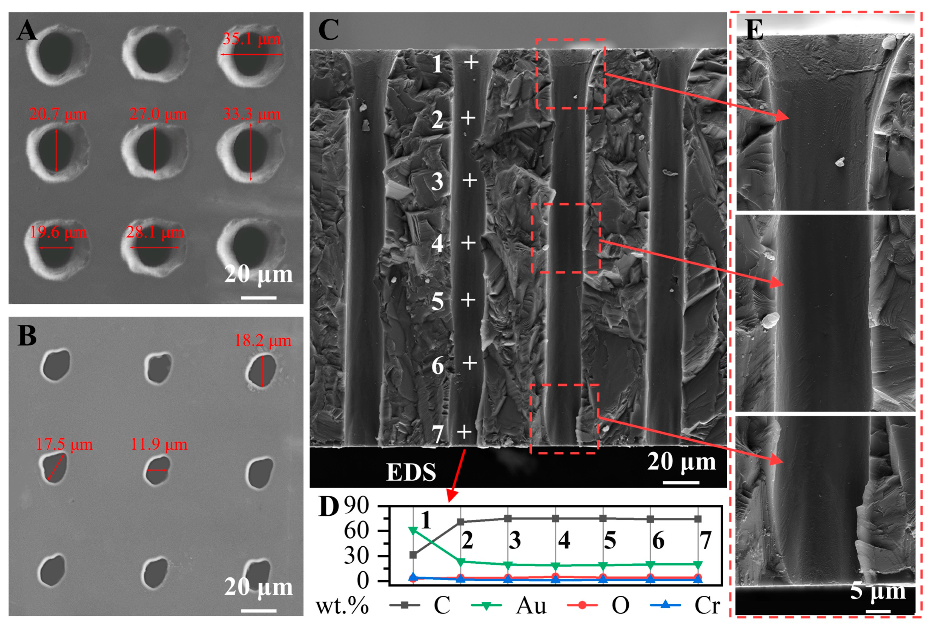
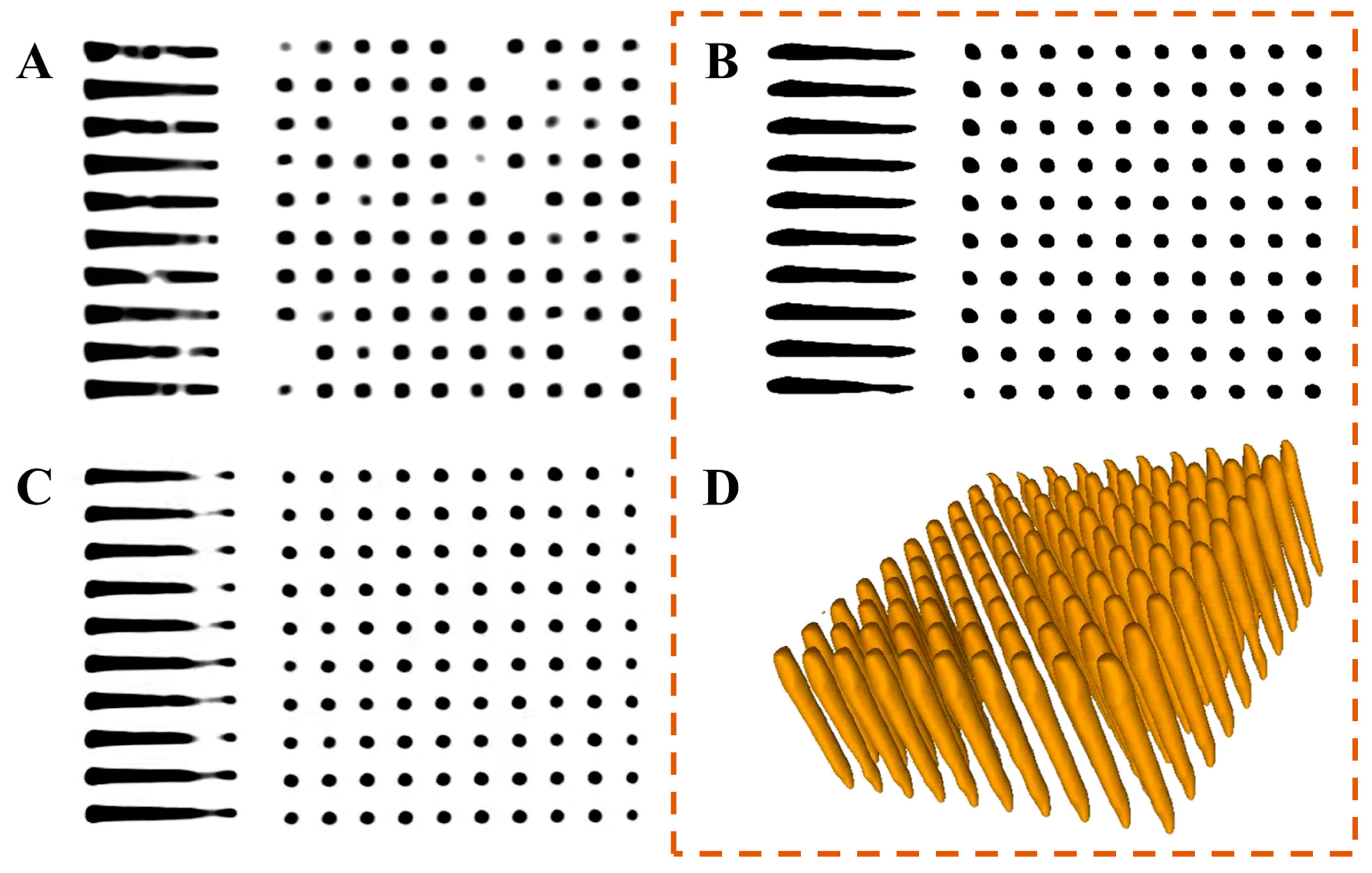
3.1. Morphology of the TDV
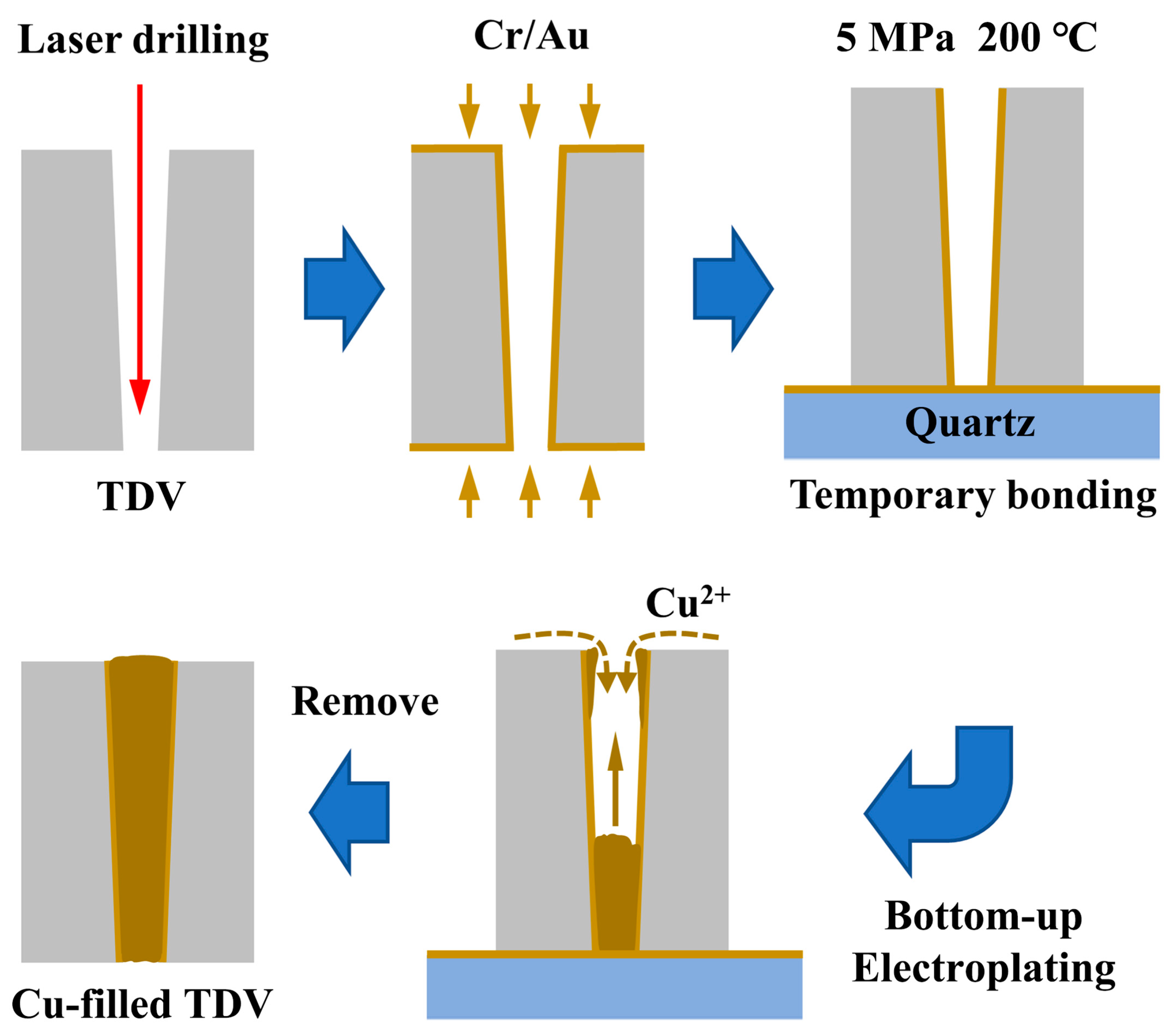
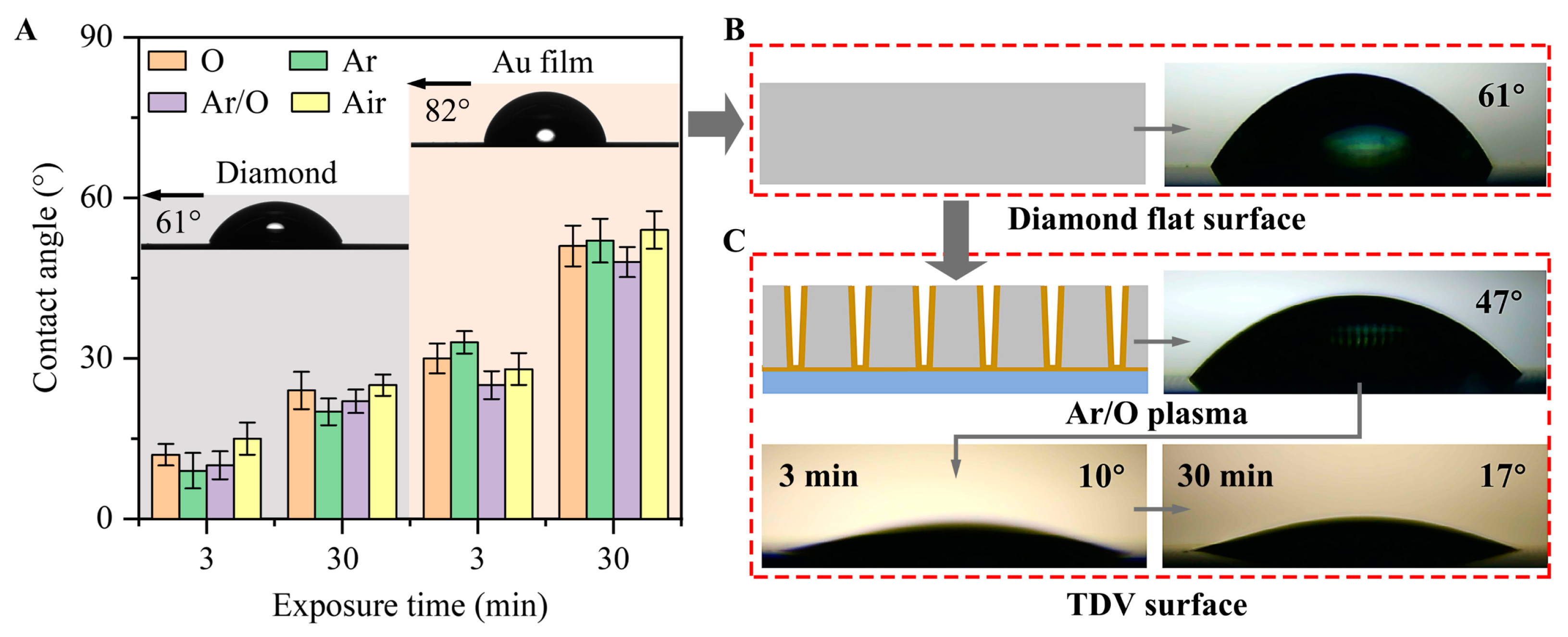
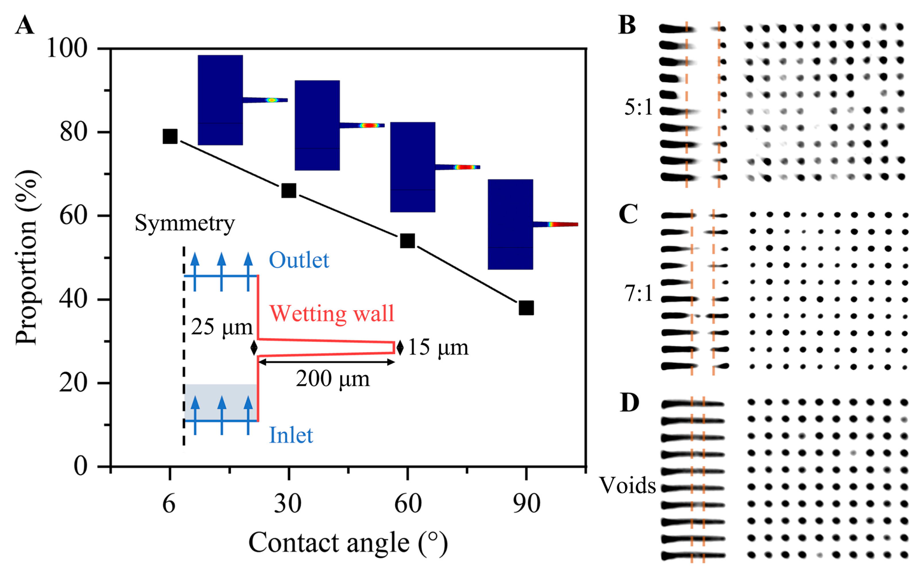
3.2. Bottom-Up Cu Electroplating Process
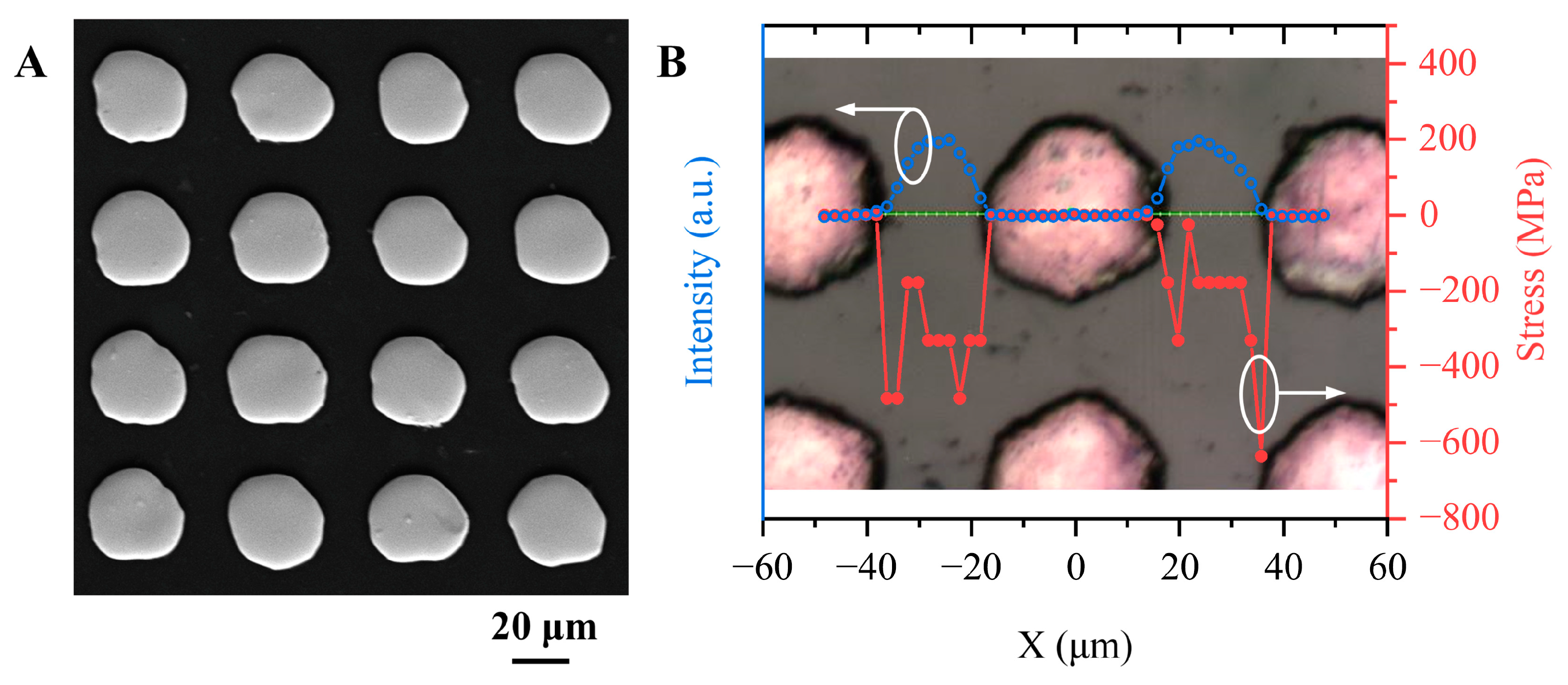
3.3. Raman Measurement of Cu-Filled TDV
3.4. Resistance Measurement of the Cu-Filled TDV
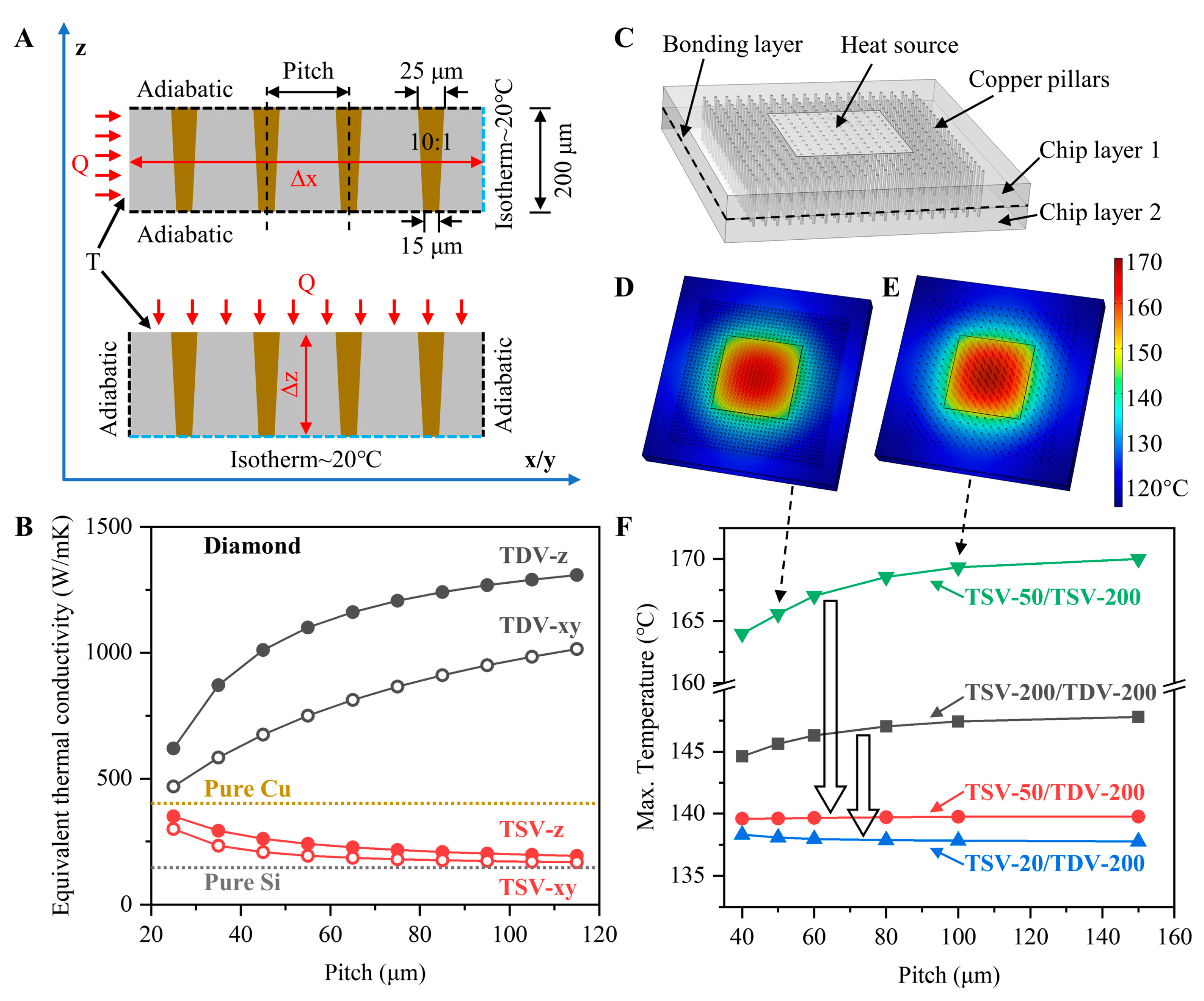
3.5. Thermal Analysis Simulation
4. Conclusions
Author Contributions
Funding
Data Availability Statement
Acknowledgments
Conflicts of Interest
References
- Zhang, S. Review of Modern Field Effect Transistor Technologies for Scaling. J. Phys. Conf. Ser. 2020, 1617. [Google Scholar] [CrossRef]
- Ko, C.T.; Chen, K.N. Wafer-Level bonding/stacking technology for 3D integration. Microelectron. Reliab. 2010, 50, 481–488. [Google Scholar] [CrossRef]
- Zhou, S.; Liu, X.; Yan, H.; Chen, Z.; Liu, Y.; Liu, S. Highly Efficient GaN-Based High-Power Flip- Chip Light-Emitting Diodes. Opt. Express 2019, 27, 669–692. [Google Scholar] [CrossRef] [PubMed]
- Li, C.; Wang, X.; Song, S.; Liu, S. 21-layer 3D chip stacking based on Cu-Sn bump bonding. IEEE Trans. Componen. Packag. Manuf. Technol. 2015, 5, 627–635. [Google Scholar] [CrossRef]
- Liu, B.; Bi, T.; Fu, Y.; Kudara, K.; Imanishi, S.; Liu, K.; Dai, B.; Zhu, J.; Kawarada, H. MOSFETs on (110) C–H Diamond: ALD Al2O3/Diamond Interface Analysis and High Performance Normally-OFF Operation Realization. IEEE Trans. Electron. Devices 2022, 69, 949–955. [Google Scholar] [CrossRef]
- Wang, Z. Microsystems Using Three-Dimensional Integration and TSV Technologies: Fundamentals and Applications. Microelectron. Eng. 2019, 210, 35–64. [Google Scholar] [CrossRef]
- Xu, B.; Liao, Y.; Fang, Z.; Nagato, K.; Kodama, T.; Nishikawa, Y.; Shiomi, J. Ultra-high-performance heat spreader based on a graphite architecture with three-dimensional thermal routing. Cell Rep. Phys. Sci. 2021, 2, 100621. [Google Scholar] [CrossRef]
- Sun, F.L.; Liu, Z.Q.; Li, C.F.; Zhu, Q.S.; Zhang, H.; Suganuma, K. Bottom-up electrodeposition of large-scale nanotwinned copper within 3D through silicon via. Materials 2018, 11, 319. [Google Scholar] [CrossRef]
- Ma, S.; Lian, T.; Cai, H.; Hu, L.; He, S. Thermal property evaluation of TSV interposer embedded microfluidics for cooling 2.5D integrated high power IC device. In Proceedings of the 2019 20th International Conference on Electronic Packaging Technology (ICEPT), Hong Kong, China, 12–15 August 2019. [Google Scholar] [CrossRef]
- Kandlikar, S.G. Review and projections of integrated cooling systems for three-dimensional integrated circuits. J. Electron. Packag. Trans. 2014, 136, 024001. [Google Scholar] [CrossRef]
- Vandersande, J.W.; Zoltan, L.D. High temperature electrical conductivity measurements of natural diamond and diamond films. Surf. Coat. Technol. 1991, 47, 392–400. [Google Scholar] [CrossRef]
- Sang, L. Diamond as the heat spreader for the thermal dissipation of GaN-based electronic devices. Funct. Diam. 2021, 1, 174–188. [Google Scholar] [CrossRef]
- Palko, J.W.; Lee, H.; Agonafer, D.D.; Zhang, C.; Jung, K.W.; Moss, J.; Wilbur, J.D.; Dusseault, T.J.; Barako, M.T.; Houshmand, F.; et al. High heat flux two-phase cooling of electronics with integrated diamond/porous copper heat sinks and microfluidic coolant supply. In Proceedings of the 15th IEEE Intersociety Conference on Thermal and Thermomechanical Phenomena in Electronic Systems (ITherm), Las Vegas, NV, USA, 31 May–3 June 2016; pp. 1511–1517. [Google Scholar] [CrossRef]
- Han, Y.; Lau, B.L.; Zhang, X.; Leong, Y.C.; Choo, K.F. Thermal management of hotspots with a microjet-based hybrid heat sink for GaN-on-Si devices. IEEE Trans. Compon. Packag. Manuf. Technol. 2014, 4, 1441–1450. [Google Scholar] [CrossRef]
- Kang, Q.; Wang, C.; Zhou, S.; Li, G.; Lu, T.; Tian, Y.; He, P. Low-temperature Co-hydroxylated Cu/SiO2 hybrid bonding strategy for a memory-centric chip architecture. ACS Appl. Mater. Interfaces 2021, 13, 38866–38876. [Google Scholar] [CrossRef] [PubMed]
- Oprins, H.; Cherman, V.; Webers, T.; Kim, S.W.; De Vos, J.; Van Der Plas, G.; Beyne, E. 3D wafer-to-wafer bonding thermal resistance comparison: Hybrid Cu/dielectric bonding versus dielectric via-last bonding. In Proceedings of the 2020 19th IEEE Intersociety Conference on Thermal and Thermomechanical Phenomena in Electronic Systems (ITherm), Orlando, FL, USA, 21–23 July 2020; pp. 219–228. [Google Scholar] [CrossRef]
- Inoue, F.; Derakhshandeh, J.; Lofrano, M.; Beyne, E. Fine-pitch bonding technology with surface-planarized solder micro-bump/polymer hybrid for 3D integration. Jpn. J. Appl. Phys. 2021, 60, 026502. [Google Scholar] [CrossRef]
- Yu, J.; Gopinath, S.; Nalla, P.; Thorum, M.; Schloss, L.; Anjos, D.M.; Meshram, P.; Harm, G.; Richardson, J.; Mountsier, T. Advanced integrated metallization enables 3D-IC TSV scaling. In Proceedings of the 2015 IEEE International Interconnect Technology Conference and 2015 IEEE Materials for Advanced Metallization Conference (IITC/MAM), Grenoble, France, 18–21 May 2015; pp. 205–207. [Google Scholar] [CrossRef]
- Arnaud, L.; Karam, C.; Bresson, N.; Dubarry, C.; Borel, S.; Assous, M.; Mauguen, G.; Fournel, F.; Gottardi, M.; Mourier, T.; et al. Three-dimensional hybrid bonding integration challenges and solutions toward multi-wafer stacking. MRS Commun. 2020, 10, 549–557. [Google Scholar] [CrossRef]
- Minoura, Y.; Ohki, T.; Okamoto, N.; Sato, M.; Ozaki, S.; Yamada, A.; Kotani, J. GaN MMICs on a diamond heat spreader with through-substrate vias fabricated by deep dry etching process. Appl. Phys. Express 2022, 15, 036501. [Google Scholar] [CrossRef]
- Liao, Y.; Zhang, F.; Wang, P.; Xie, X.; Zhou, Y.; Xie, D. Experimental study on fabricating micro-hole arrays on CVD diamond film using a nanosecond pulsed laser. J. Superhard Mater. 2021, 43, 248–260. [Google Scholar] [CrossRef]
- Yamamoto, M.; Matsumae, T.; Kurashima, Y.; Takagi, H.; Suga, T.; Itoh, T.; Higurashi, E. Comparison of argon and oxygen plasma treatments for ambient room-temperature wafer-scale Au-Au bonding using ultrathin Au films. Micromachines 2019, 10, 119. [Google Scholar] [CrossRef]
- Kong, J.; Yung, K.L.; Xu, Y.; Tian, W. Wettability transition of plasma-treated polystyrene micro/nano pillars-aligned patterns. Express Polym. Lett. 2010, 4, 753–762. [Google Scholar] [CrossRef]
- Li, C.; Nie, J.; Zou, J.; Liu, S.; Zheng, H.; Fei, P. A new prewetting process of through silicon vias (TSV) electroplating for 3D integration. J. Microelectromechanical Syst. 2019, 28, 447–452. [Google Scholar] [CrossRef]
- Wang, F.; Zhang, Q.; Liu, W.; Wang, Y.; Zhu, W. Interaction effect of suppressor concentration and current density on the copper deposition rate in TSV filling process. Microelectron. Eng. 2019, 216, 111022. [Google Scholar] [CrossRef]
- Erasmus, R.M.; Comins, J.D.; Mofokeng, V.; Martin, Z. Application of Raman spectroscopy to determine stress in polycrystalline diamond tools as a function of tool geometry and temperature. Diam. Relat. Mater. 2011, 20, 907–911. [Google Scholar] [CrossRef]
- Chung, H.; Tu, C.M.; Lwo, B.J.; Lee, C.Y. A complete resistance extraction methodology and circuit models for typical TSV structures. Int. J. Electron. 2013, 100, 1256–1269. [Google Scholar] [CrossRef]
- Lau, J.H.; Yue, T.G. Thermal management of 3D IC integration with TSV (through silicon via). In Proceedings of the 2009 59th Electronic Components and Technology Conference, San Diego, CA, USA, 26–29 May 2009; pp. 624–640. [Google Scholar] [CrossRef]

Disclaimer/Publisher’s Note: The statements, opinions and data contained in all publications are solely those of the individual author(s) and contributor(s) and not of MDPI and/or the editor(s). MDPI and/or the editor(s) disclaim responsibility for any injury to people or property resulting from any ideas, methods, instructions or products referred to in the content. |
© 2023 by the authors. Licensee MDPI, Basel, Switzerland. This article is an open access article distributed under the terms and conditions of the Creative Commons Attribution (CC BY) license (https://creativecommons.org/licenses/by/4.0/).
Share and Cite
Zhao, K.; Zhao, J.; Wei, X.; Guan, X.; Deng, C.; Dai, B.; Zhu, J. Bottom-Up Cu Filling of High-Aspect-Ratio through-Diamond vias for 3D Integration in Thermal Management. Micromachines 2023, 14, 290. https://doi.org/10.3390/mi14020290
Zhao K, Zhao J, Wei X, Guan X, Deng C, Dai B, Zhu J. Bottom-Up Cu Filling of High-Aspect-Ratio through-Diamond vias for 3D Integration in Thermal Management. Micromachines. 2023; 14(2):290. https://doi.org/10.3390/mi14020290
Chicago/Turabian StyleZhao, Kechen, Jiwen Zhao, Xiaoyun Wei, Xiaoyu Guan, Chaojun Deng, Bing Dai, and Jiaqi Zhu. 2023. "Bottom-Up Cu Filling of High-Aspect-Ratio through-Diamond vias for 3D Integration in Thermal Management" Micromachines 14, no. 2: 290. https://doi.org/10.3390/mi14020290
APA StyleZhao, K., Zhao, J., Wei, X., Guan, X., Deng, C., Dai, B., & Zhu, J. (2023). Bottom-Up Cu Filling of High-Aspect-Ratio through-Diamond vias for 3D Integration in Thermal Management. Micromachines, 14(2), 290. https://doi.org/10.3390/mi14020290


