
Optoelectronic Enhancement of Perovskite Solar Cells through the Incorporation of Plasmonic Particles

 and
and 
Abstract
:1. Introduction
2. Experimental Details
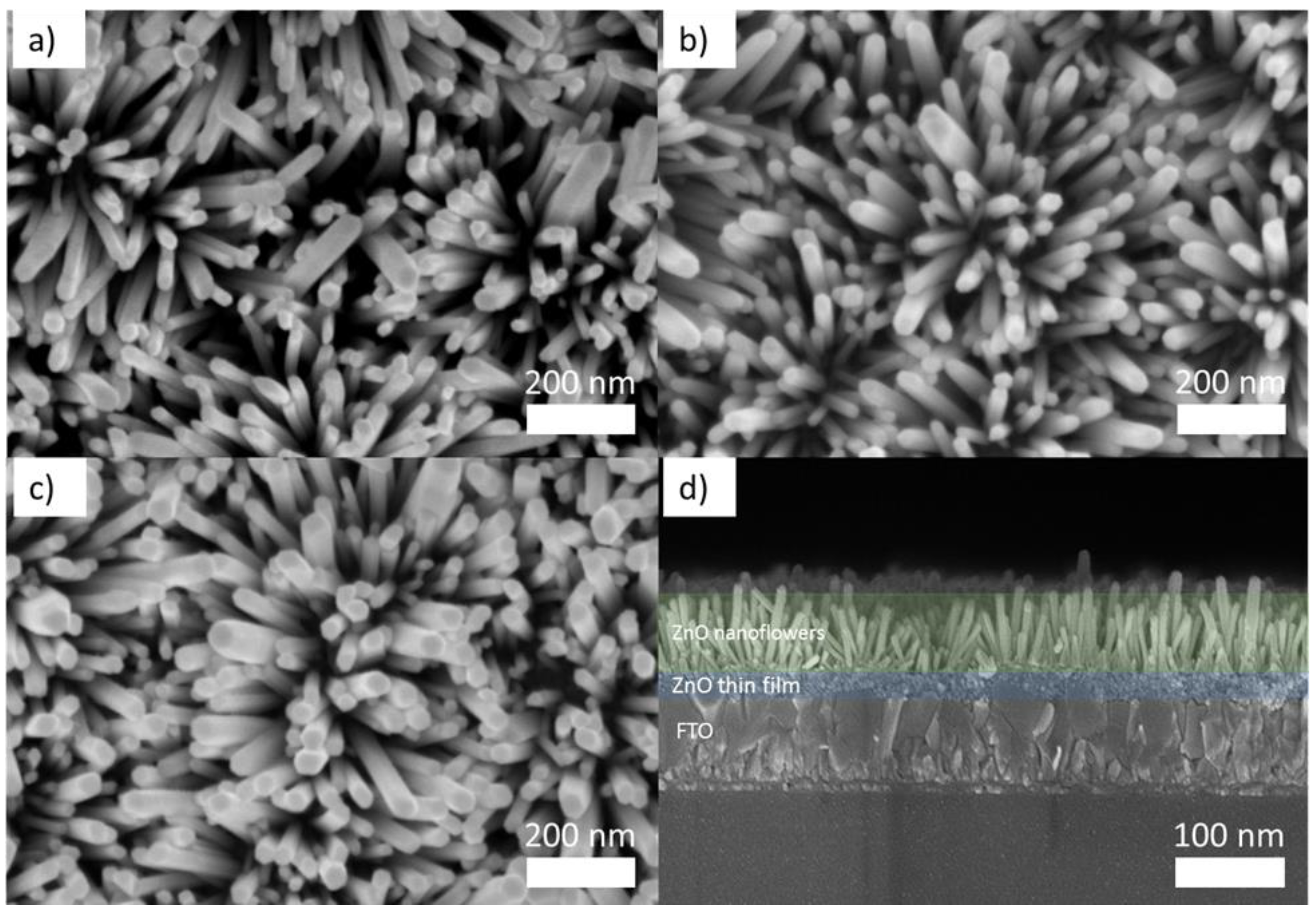
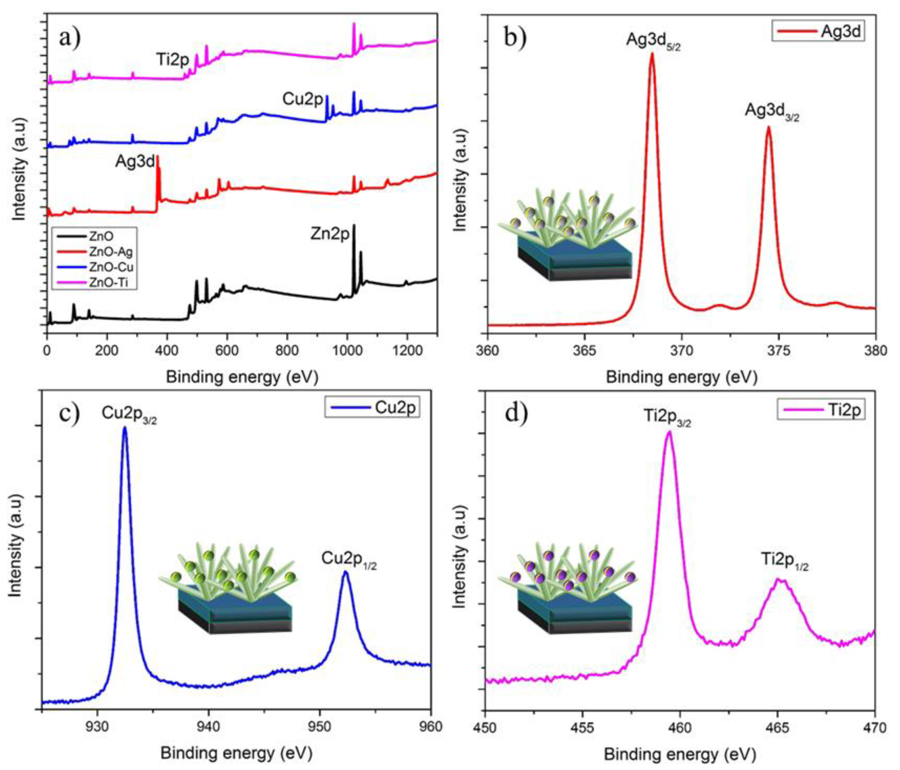
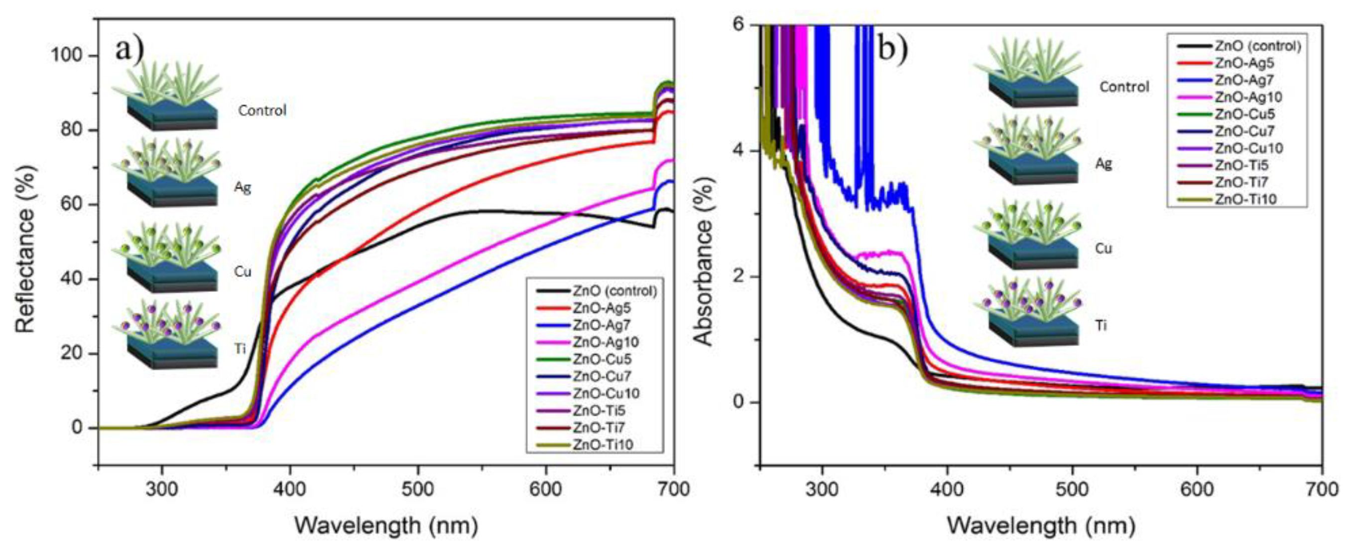
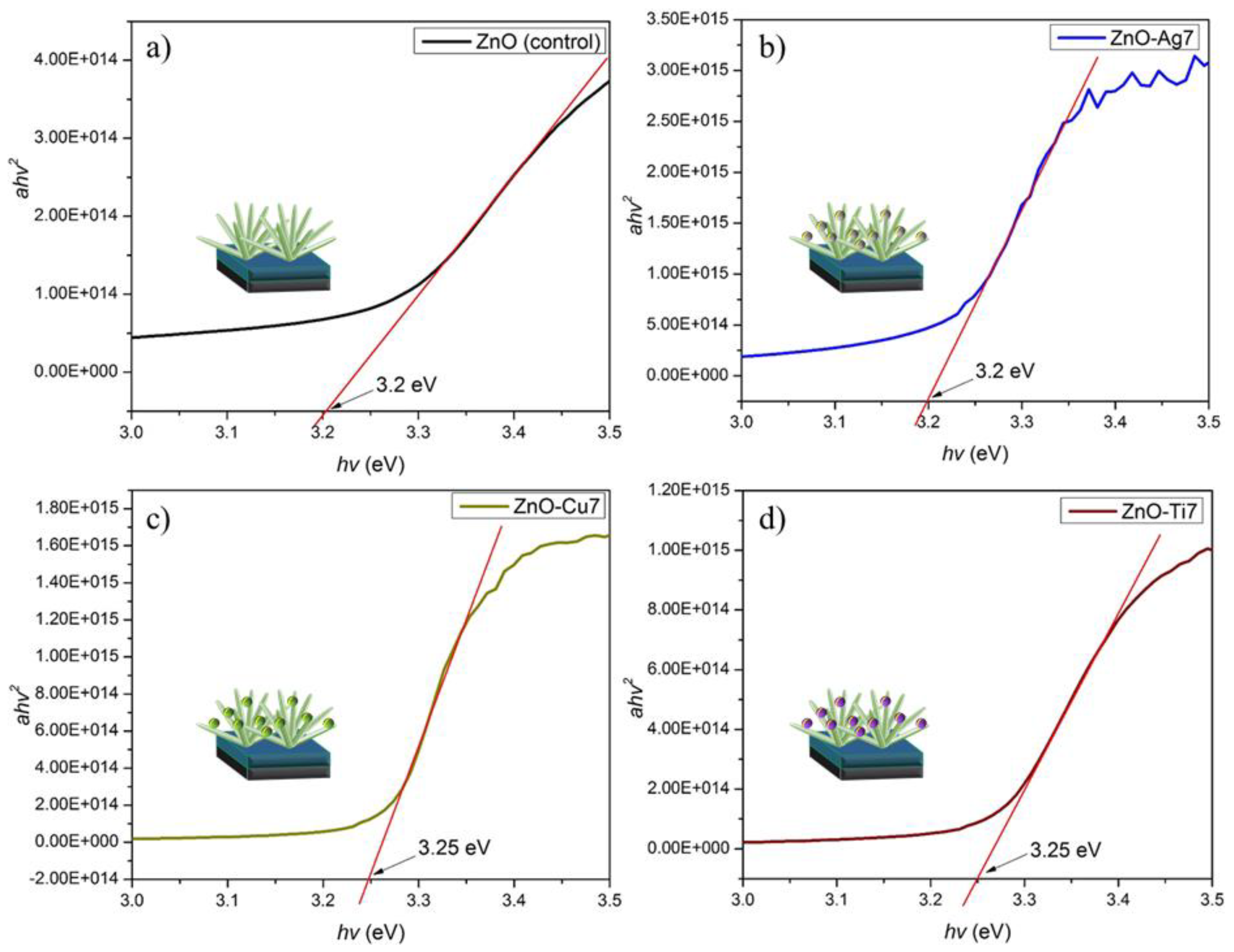
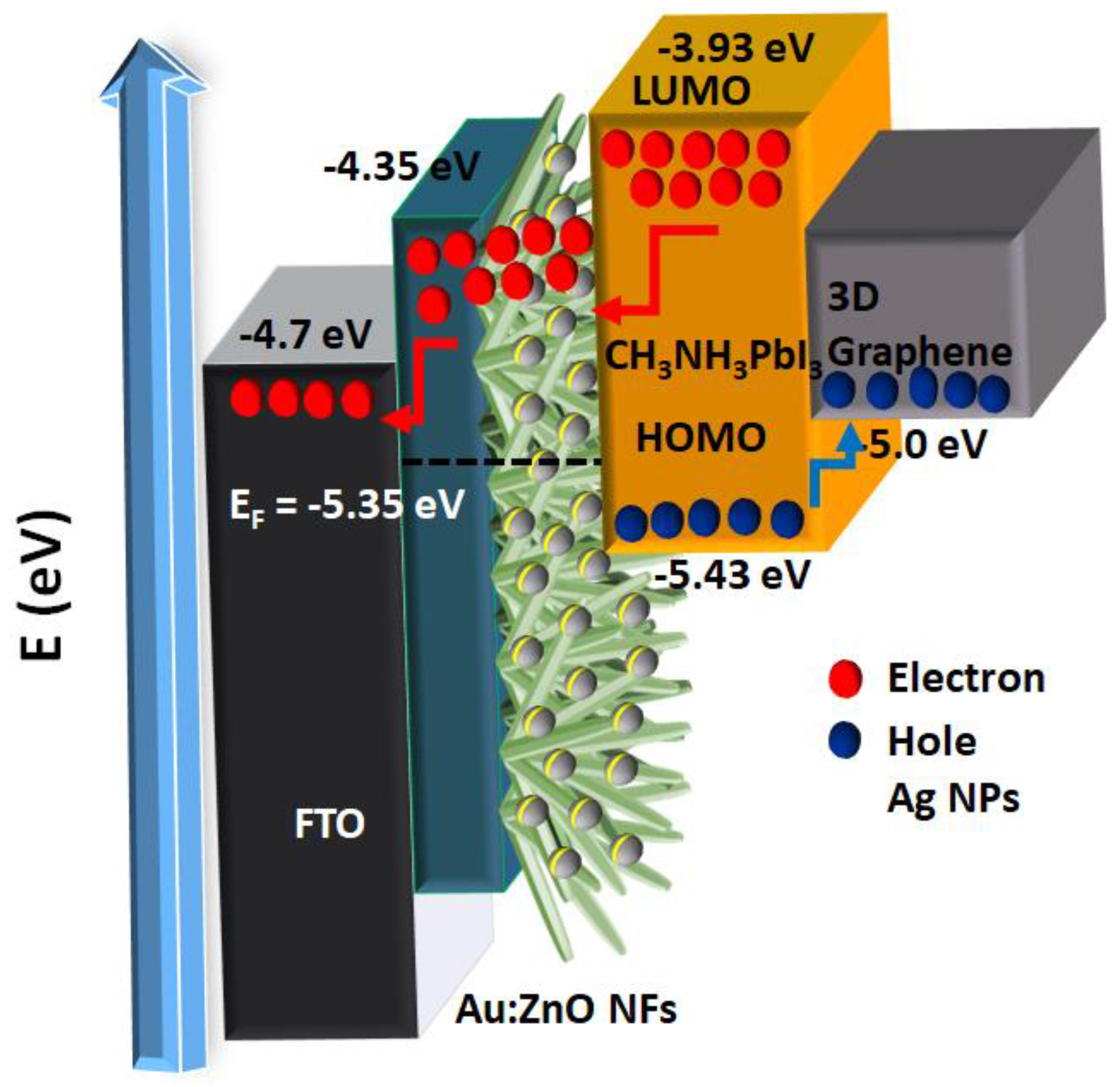
3. Results and Discussion
4. Conclusions
Supplementary Materials
Author Contributions
Funding
Institutional Review Board Statement
Informed Consent Statement
Data Availability Statement
Acknowledgments
Conflicts of Interest
References
- Ling, J.; Wali, Q.; Al-Douri, Y.; Jose, R. Fundamental of Solar Cells. In Renewable Energy: Analysis, Resources, Applications, Management, and Policy; Al-Douri, Y., Ed.; AIP Publishing: Melville, NY, USA, 2022; Volume 1, pp. 5-1–5-26. [Google Scholar]
- Elumalai, N.K.; Mahmud, M.A.; Wang, D.; Uddin, A. Perovskite solar cells: Progress and advancements. Energies 2016, 9, 861. [Google Scholar] [CrossRef] [Green Version]
- Fakharuddin, A.; Schmidt-Mende, L.; Garcia-Belmonte, G.; Jose, R.; Mora-Sero, I. Interfaces in Perovskite Solar Cells. Adv. Energy Mater. 2017, 7, 1700623. [Google Scholar] [CrossRef]
- Ling, J.; Kizhakkedath, P.K.K.; Watson, T.M.; Mora-Seró, I.; Schmidt-Mende, L.; Brown, T.M.; Jose, R. A Perspective on the Commercial Viability of Perovskite Solar Cells. Solar RRL 2021, 5, 2100401. [Google Scholar] [CrossRef]
- Iftikhar, F.J.; Wali, Q.; Yang, S.; Iqbal, Y.; Jose, R.; Munir, S.; Gondal, I.A.; Khan, M.E. Structural and optoelectronic properties of hybrid halide perovskites for solar cells. Org. Electron. 2021, 91, 106077. [Google Scholar] [CrossRef]
- Mahmud, M.A.; Duong, T.; Peng, J.; Wu, Y.; Shen, H.; Walter, D.; Nguyen, H.T.; Mozaffari, N.; Tabi, G.D.; Catchpole, K.R.; et al. Origin of Efficiency and Stability Enhancement in High-Performing Mixed Dimensional 2D-3D Perovskite Solar Cells: A Review. Adv. Funct. Mater. 2022, 32, 2009164. [Google Scholar] [CrossRef]
- Kojima, A.; Teshima, K.; Shirai, Y.; Miyasaka, T. Organometal halide perovskites as visible-light sensitizers for photovoltaic cells. J. Am. Chem. Soc. 2009, 131, 6050–6051. [Google Scholar] [CrossRef]
- Zheng, L.; Shen, L.; Zhu, T.; Zhang, D.; Zheng, J.; Gong, X. Stable and efficient perovskite solar cells by discrete two-dimensional perovskites capped on the three-dimensional perovskites bilayer thin film. Nano Energy 2022, 96, 107126. [Google Scholar] [CrossRef]
- Zhu, T.; Shen, L.; Xun, S.; Sarmiento, J.S.; Yang, Y.; Zheng, L.; Li, H.; Wang, H.; Bredas, J.L.; Gong, X. High-Performance Ternary Perovskite–Organic Solar Cells. Adv. Mater. 2022, 34, 2109348. [Google Scholar] [CrossRef]
- Chen, J.; He, D.; Park, N.G. Methodologies for >30% Efficient Perovskite Solar Cells via Enhancement of Voltage and Fill Factor. Solar RRL 2022, 6, 2100767. [Google Scholar] [CrossRef]
- Yang, S.; Han, Q.; Wang, L.; Zhou, Y.; Yu, F.; Li, C.; Cai, X.; Gao, L.; Zhang, C.; Ma, T. Over 23% power conversion efficiency of planar perovskite solar cells via bulk heterojunction design. Chem. Eng. J. 2021, 426, 131838. [Google Scholar] [CrossRef]
- Kaltenbrunner, M.; Adam, G.; Głowacki, E.D.; Drack, M.; Schwödiauer, R.; Leonat, L.; Apaydin, D.H.; Groiss, H.; Scharber, M.C.; White, M.S.; et al. Flexible high power-per-weight perovskite solar cells with chromium oxide-metal contacts for improved stability in air. Nat. Mater. 2015, 14, 1032–1039. [Google Scholar] [CrossRef] [PubMed]
- Oga, H.; Saeki, A.; Ogomi, Y.; Hayase, S.; Seki, S. Improved understanding of the electronic and energetic landscapes of perovskite solar cells: High local charge carrier mobility, reduced recombination, and extremely shallow traps. J. Am. Chem. Soc. 2014, 136, 13818–13825. [Google Scholar] [CrossRef]
- Gao, P.; Bin Mohd Yusoff, A.R.; Nazeeruddin, M.K. Dimensionality engineering of hybrid halide perovskite light absorbers. Nat. Commun. 2018, 9, 5028. [Google Scholar] [CrossRef] [PubMed] [Green Version]
- Zhao, W.; Xu, J.; He, K.; Cai, Y.; Han, Y.; Yang, S.; Zhan, S.; Wang, D.; Liu, Z.; Liu, S. A Special Additive Enables All Cations and Anions Passivation for Stable Perovskite Solar Cells with Efficiency over 23%. Nano-Micro Lett. 2021, 13, 169. [Google Scholar] [CrossRef]
- Santhosh, N.; Daniel, R.I.; Acchutharaman, K.R.; Pandian, M.S.; Ramasamy, P. Enhanced performance of hole-conductor free carbon-based perovskite solar cells through polyvinylidene fluoride as additive. Mater. Today Commun. 2022, 31, 103446. [Google Scholar] [CrossRef]
- Arjmand, F.; Golshani, Z.; Fatemi, S.J.; Maghsoudi, S.; Naeimi, A.; Hosseini, S.M.A. The lead-free perovskite solar cells with the green synthesized BiI3 and AgI nanoparticles using Vitex agnus-castus plant extract for HTM-free and carbon-based solar cells. J. Mater. Res. Technol. 2022, 18, 1922–1933. [Google Scholar] [CrossRef]
- Bakr, Z.H.; Wali, Q.; Fakharuddin, A.; Schmidt-Mende, L.; Brown, T.M.; Jose, R. Advances in hole transport materials engineering for stable and efficient perovskite solar cells. Nano Energy 2017, 34, 271–305. [Google Scholar] [CrossRef] [Green Version]
- Dong, Q.; Chen, M.; Liu, Y.; Eickemeyer, F.T.; Zhao, W.; Dai, Z.; Yin, Y.; Jiang, C.; Feng, J.; Jin, S.; et al. Flexible perovskite solar cells with simultaneously improved efficiency, operational stability, and mechanical reliability. Joule 2021, 5, 1587–1601. [Google Scholar] [CrossRef]
- Dong, Q.; Zhu, C.; Chen, M.; Jiang, C.; Guo, J.; Feng, Y.; Dai, Z.; Yadavalli, S.K.; Hu, M.; Cao, X.; et al. Interpenetrating interfaces for efficient perovskite solar cells with high operational stability and mechanical robustness. Nat. Commun. 2021, 12, 973. [Google Scholar] [CrossRef]
- Fakharuddin, A.; Di Giacomo, F.; Ahmed, I.; Wali, Q.; Brown, T.M.; Jose, R. Role of morphology and crystallinity of nanorod and planar electron transport layers on the performance and long term durability of perovskite solar cells. J. Power Sources 2015, 283, 61–67. [Google Scholar] [CrossRef] [Green Version]
- Sun, X.; Wu, F.; Zhong, C.; Zhu, L.; Li, Z. A structure—Property study of fluoranthene-cored hole-transporting materials enables 19.3% efficiency in dopant-free perovskite solar cells. Chem. Sci. 2019, 10, 6899–6907. [Google Scholar] [CrossRef] [PubMed] [Green Version]
- Babu, V.; Fuentes Pineda, R.; Ahmad, T.; Alvarez, A.O.; Castriotta, L.A.; Di Carlo, A.; Fabregat-Santiago, F.; Wojciechowski, K. Improved Stability of Inverted and Flexible Perovskite Solar Cells with Carbon Electrode. ACS Appl. Energy Mater. 2020, 3, 5126–5134. [Google Scholar] [CrossRef]
- Huang, C.; Lin, P.; Fu, N.; Liu, C.; Xu, B.; Sun, K.; Wang, D.; Zeng, X.; Ke, S. Facile fabrication of highly efficient ETL-free perovskite solar cells with 20% efficiency by defect passivation and interface engineering. Chem. Commun. 2019, 55, 2777–2780. [Google Scholar] [CrossRef] [PubMed]
- Wu, W.-Q.; Wang, Q.; Fang, Y.; Shao, Y.; Tang, S.; Deng, Y.; Lu, H.; Liu, Y.; Li, T.; Yang, Z.; et al. Molecular doping enabled scalable blading of efficient hole-transport-layer-free perovskite solar cells. Nat. Commun. 2018, 9, 1625. [Google Scholar] [CrossRef] [PubMed]
- Chen, H.N.; Wei, Z.H.; He, H.X.; Zheng, X.L.; Wong, K.S.; Yang, S.H. Solvent Engineering Boosts the Efficiency of Paintable Carbon-Based Perovskite Solar Cells to beyond 14%. Adv. Energy Mater. 2016, 6, 1502087. [Google Scholar] [CrossRef]
- Chen, Q.; Zhou, H.; Hong, Z.; Luo, S.; Duan, H.-S.; Wang, H.-H.; Liu, Y.; Li, G.; Yang, Y. Planar Heterojunction Perovskite Solar Cells via Vapor-Assisted Solution Process. J. Am. Chem. Soc. 2014, 136, 622–625. [Google Scholar] [CrossRef]
- Chen, S.; Lei, L.; Yang, S.; Liu, Y.; Wang, Z.-S. Characterization of Perovskite Obtained from Two-Step Deposition on Mesoporous Titania. ACS Appl. Mater. Interfaces 2015, 7, 25770–25776. [Google Scholar] [CrossRef]
- Leyden, M.R.; Jiang, Y.; Qi, Y. Chemical vapor deposition grown formamidinium perovskite solar modules with high steady state power and thermal stability. J. Mater. Chem. A 2016, 4, 13125–13132. [Google Scholar] [CrossRef] [Green Version]
- Mitzi, D.B.; Prikas, M.T.; Chondroudis, K. Thin Film Deposition of Organic-Inorganic Hybrid Materials Using a Single Source Thermal Ablation Technique. Chem. Mater. 1999, 11, 542–544. [Google Scholar] [CrossRef]
- Tavakoli, M.M.; Gu, L.; Gao, Y.; Reckmeier, C.; He, J.; Rogach, A.L.; Yao, Y.; Fan, Z. Fabrication of efficient planar perovskite solar cells using a one-step chemical vapor deposition method. Sci. Rep. 2015, 5, 14083. [Google Scholar] [CrossRef]
- Chen, L.C.; Lee, K.L.; Huang, C.Y.; Lin, J.C.; Tseng, Z.L. Preparation and characteristics of MAPbBr3 perovskite quantum dots on NiOx film and application for high transparent solar cells. Micromachines 2018, 9, 205. [Google Scholar] [CrossRef] [Green Version]
- Dagar, J.; Paramasivam, G.; Klimm, C.; Fenske, M.; Schultz, C.; Schlatmann, R.; Stegemann, B.; Unger, E. Stability assessment of p-i-n perovskite photovoltaic mini-modules utilizing different top metal electrodes. Micromachines 2021, 12, 423. [Google Scholar] [CrossRef] [PubMed]
- Di Giacomo, F.; Castriotta, L.A.; Kosasih, F.U.; Di Girolamo, D.; Ducati, C.; Di Carlo, A. Upscaling inverted perovskite solar cells: Optimization of laser scribing for highly efficient mini-modules. Micromachines 2020, 11, 1127. [Google Scholar] [CrossRef] [PubMed]
- Raminafshar, C.; Raptis, D.; Mohammadi, M.R.; Lianos, P. Study of hole-transporter-free perovskite solar cells based on fully printable components. Micromachines 2019, 10, 266. [Google Scholar] [CrossRef] [Green Version]
- Vrakatseli, V.E.; Kalarakis, A.N.; Kalampounias, A.G.; Amanatides, E.K.; Mataras, D.S. Glancing angle deposition effect on structure and light-induced wettability of RF-sputtered TiO2 thin films. Micromachines 2018, 9, 389. [Google Scholar] [CrossRef] [Green Version]
- Zhou, P.; Li, W.; Li, T.; Bu, T.; Liu, X.; Li, J.; He, J.; Chen, R.; Li, K.; Zhao, J.; et al. Ultrasonic spray-coating of large-scale TiO2 compact layer for efficient flexible perovskite solar cells. Micromachines 2017, 8, 55. [Google Scholar] [CrossRef] [Green Version]
- Bag, A.; Radhakrishnan, R.; Nekovei, R.; Jeyakumar, R. Effect of absorber layer, hole transport layer thicknesses, and its doping density on the performance of perovskite solar cells by device simulation. Sol. Energy 2020, 196, 177–182. [Google Scholar] [CrossRef]
- Rai, M.; Wong, L.H.; Etgar, L. Effect of Perovskite Thickness on Electroluminescence and Solar Cell Conversion Efficiency. J. Phys. Chem. Lett. 2020, 11, 8189–8194. [Google Scholar] [CrossRef]
- Du, T.; Xu, W.; Xu, S.; Ratnasingham, S.R.; Lin, C.-T.; Kim, J.; Briscoe, J.; McLachlan, M.A.; Durrant, J.R. Light-intensity and thickness dependent efficiency of planar perovskite solar cells: Charge recombination versus extraction. J. Mater. Chem. C 2020, 8, 12648–12655. [Google Scholar] [CrossRef]
- Mohamed Saheed, M.S.; Mohamed, N.M.; Mahinder Singh, B.S.; Wali, Q.; Saheed, M.S.M.; Jose, R. Foam-like 3D Graphene as a Charge Transport Modifier in Zinc Oxide Electron Transport Material in Perovskite Solar Cells. Photochem 2021, 1, 523–536. [Google Scholar] [CrossRef]
- Ai, B.; Fan, Z.; Wong, Z.J. Plasmonic–Perovskite solar cells, light emitters, and sensors. Microsyst. Nanoeng. 2022, 8, 5. [Google Scholar] [CrossRef] [PubMed]
- Mohamed Saheed, M.S.; Mohamed, N.M.; Mahinder Singh, B.S.; Jose, R. Surface Plasmon Assisted Electron–Hole Migration for High Photocurrent Density Generation in a Perovskite Solar Cell. ACS Appl. Energy Mater. 2019, 2, 8707–8714. [Google Scholar] [CrossRef]
- Cheng, C.J.; Balamurugan, R.; Liu, B.T. Enhanced efficiencies of perovskite solar cells by incorporating silver nanowires into the hole transport layer. Micromachines 2019, 10, 682. [Google Scholar] [CrossRef] [Green Version]
- Jacak, J.E.; Jacak, W.A. Routes for Metallization of Perovskite Solar Cells. Materials 2022, 15, 2254. [Google Scholar] [CrossRef]
- Lie, S.; Bruno, A.; Wong, L.H.; Etgar, L. Semitransparent Perovskite Solar Cells with >13% Efficiency and 27% Transperancy Using Plasmonic Au Nanorods. ACS Appl. Mater. Interfaces 2022, 14, 11339–11349. [Google Scholar] [CrossRef] [PubMed]
- Talebi, H.; Emami, F. Broadband plasmonic absorption enhancement of perovskite solar cells with embedded Au@SiO2@graphene core-shell nanoparticles. Semicond. Sci. Technol. 2022, 37, 055002. [Google Scholar] [CrossRef]
- Wu, Y.; Sun, X.; Dai, S.; Li, M.; Zheng, L.; Wen, Q.; Tang, B.; Yun, D.Q.; Xiao, L. Broad-Band-Enhanced Plasmonic Perovskite Solar Cells with Irregular Silver Nanomaterials. ACS Appl. Mater. Interfaces 2022, 14, 16269–16278. [Google Scholar] [CrossRef] [PubMed]
- Shen, T.; Tan, Q.; Dai, Z.; Padture, N.P.; Pacifici, D. Arrays of plasmonic nanostructures for absorption enhancement in perovskite thin films. Nanomaterials 2020, 10, 1342. [Google Scholar] [CrossRef]
- Song, D.H.; Kim, H.S.; Suh, J.S.; Jun, B.H.; Rho, W.Y. Multi-shaped Ag nanoparticles in the plasmonic layer of dye-sensitized solar cells for increased power conversion efficiency. Nanomaterials 2017, 7, 136. [Google Scholar] [CrossRef]
- Wang, B.; Zhu, X.; Li, S.; Chen, M.; Liu, N.; Yang, H.; Ran, M.; Lu, H.; Yang, Y. Enhancing the photovoltaic performance of perovskite solar cells using plasmonic Au@Pt@Au core-shell nanoparticles. Nanomaterials 2019, 9, 1263. [Google Scholar] [CrossRef] [Green Version]
- Xia, Z.; Zhang, C.; Feng, Z.; Wu, Z.; Wang, Z.; Chen, X.; Huang, S. Synergetic effect of plasmonic gold nanorods and mgo for perovskite solar cells. Nanomaterials 2020, 10, 1830. [Google Scholar] [CrossRef] [PubMed]
- Irandoost, R.; Soleimani-Amiri, S. Design and analysis of high efficiency perovskite solar cell with ZnO nanorods and plasmonic nanoparticles. Optik 2020, 202, 163598. [Google Scholar] [CrossRef]
- Chen, Z.; Deng, C.; Xi, X.; Chen, Y.; Feng, Y.; Jiang, S.; Chen, W.; Kang, X.; Wang, Q.; Zhang, G.; et al. Study on localized surface plasmon coupling with many radiators. Nanomaterials 2021, 11, 3105. [Google Scholar] [CrossRef] [PubMed]
- Gaur, R.; Manikandan, P.; Manikandan, D.; Umapathy, S.; Padhy, H.M.; Maaza, M.; Elayaperumal, M. Noble Metal Ion Embedded Nanocomposite Glass Materials for Optical Functionality of UV–Visible Surface Plasmon Resonance (SPR) Surface-Enhanced Raman Scattering (SERS) X-ray and Electron Microscopic Studies: An Overview. Plasmonics 2021, 16, 1461–1493. [Google Scholar] [CrossRef]
- Hang, Y.; Boryczka, J.; Wu, N. Visible-light and near-infrared fluorescence and surface-enhanced Raman scattering point-of-care sensing and bio-imaging: A review. Chem. Soc. Rev. 2022, 51, 329–375. [Google Scholar] [CrossRef] [PubMed]
- Liu, S.; Sun, Y.; Chen, L.; Zhang, Q.; Li, X.; Shuai, J. A review on plasmonic nanostructures for efficiency enhancement of organic solar cells. Mater. Today Phys. 2022, 24, 100680. [Google Scholar] [CrossRef]
- Priest, L.; Peters, J.S.; Kukura, P. Scattering-based Light Microscopy: From Metal Nanoparticles to Single Proteins. Chem. Rev. 2021, 121, 11937–11970. [Google Scholar] [CrossRef]
- Wang, Z.; Zheng, X.; Gao, M.; Zhao, J.; Lan, J.; Ye, X.; Wan, J.; Fei, Y.; Guo, S.; Wu, Y.; et al. Plasmonic properties and sensor application of the Ag nanocaps. J. Phys. Chem. Solids 2022, 161, 110414. [Google Scholar] [CrossRef]
- Abd-Ellah, M.; Moghimi, N.; Zhang, L.; Thomas, J.P.; McGillivray, D.; Srivastava, S.; Leung, K.T. Plasmonic gold nanoparticles for ZnO-nanotube photoanodes in dye-sensitized solar cell application. Nanoscale 2016, 8, 1658–1664. [Google Scholar] [CrossRef] [PubMed]
- Bai, H.; Lam, S.H.; Yang, J.; Cheng, X.; Li, S.; Jiang, R.; Shao, L.; Wang, J. A Schottky-Barrier-Free Plasmonic Semiconductor Photocatalyst for Nitrogen Fixation in a “One-Stone-Two-Birds” Manner. Adv. Mater. 2022, 34, 2104226. [Google Scholar] [CrossRef]
- Hsu, C.L.; Lin, J.H.; Hsu, D.X.; Wang, S.H.; Lin, S.Y.; Hsueh, T.J. Enhanced non-enzymatic glucose biosensor of ZnO nanowires via decorated Pt nanoparticles and illuminated with UV/green light emitting diodes. Sens. Actuators B Chem. 2017, 238, 150–159. [Google Scholar] [CrossRef]
- Lin, L.; Feng, X.; Lan, D.; Chen, Y.; Zhong, Q.; Liu, C.; Cheng, Y.; Qi, R.; Ge, J.; Yu, C.; et al. Coupling Effect of Au Nanoparticles with the Oxygen Vacancies of TiO2- xfor Enhanced Charge Transfer. J. Phys. Chem. C 2020, 124, 23823–23831. [Google Scholar] [CrossRef]
- Novitsky, A.; Uskov, A.V.; Gritti, C.; Protsenko, I.E.; Kardynał, B.E.; Lavrinenko, A.V. Photon absorption and photocurrent in solar cells below semiconductor bandgap due to electron photoemission from plasmonic nanoantennas. Prog. Photovolt. Res. Appl. 2014, 22, 422–426. [Google Scholar] [CrossRef] [Green Version]
- Park, J.Y.; Kim, S.M.; Lee, H.; Nedrygailov, I.I. Hot-Electron-Mediated Surface Chemistry: Toward Electronic Control of Catalytic Activity. Acc. Chem. Res. 2015, 48, 2475–2483. [Google Scholar] [CrossRef]
- Schick, I.; Gehrig, D.; Montigny, M.; Balke, B.; Panthöfer, M.; Henkel, A.; Laquai, F.; Tremel, W. Effect of Charge Transfer in Magnetic-Plasmonic Au@MOx (M = Mn, Fe) Heterodimers on the Kinetics of Nanocrystal Formation. Chem. Mater. 2015, 27, 4877–4884. [Google Scholar] [CrossRef]
- Li, F.; Lo, T.W.; Deng, X.; Li, S.; Fan, Y.; Lin, F.R.; Cheng, Y.; Zhu, Z.; Lei, D.; Jen, A.K.Y. Plasmonic Local Heating Induced Strain Modulation for Enhanced Efficiency and Stability of Perovskite Solar Cells. Adv. Energy Mater. 2022, 12, 2200186. [Google Scholar] [CrossRef]
- Zhao, F.; Lin, J.; Lei, Z.; Yi, Z.; Qin, F.; Zhang, J.; Liu, L.; Wu, X.; Yang, W.; Wu, P. Realization of 18.97% theoretical efficiency of 0.9 μm thick c-Si/ZnO heterojunction ultrathin-film solar cells via surface plasmon resonance enhancement. Phys. Chem. Chem. Phys. 2022, 24, 4871–4880. [Google Scholar] [CrossRef]
- Deng, Y.; Cao, G.; Wu, Y.; Zhou, X.; Liao, W. Theoretical Description of Dynamic Transmission Characteristics in MDM Waveguide Aperture-Side-Coupled with Ring Cavity. Plasmonics 2015, 10, 1537–1543. [Google Scholar] [CrossRef]
- Chen, H.; Chen, Z.; Yang, H.; Wen, L.; Yi, Z.; Zhou, Z.; Dai, B.; Zhang, J.; Wu, X.; Wu, P. Multi-mode surface plasmon resonance absorber based on dart-type single-layer graphene. RSC Adv. 2022, 12, 7821–7829. [Google Scholar] [CrossRef]
- Chen, J.; Nie, H.; Tang, C.; Cui, Y.; Yan, B.; Zhang, Z.; Kong, Y.; Xu, Z.; Cai, P. Highly sensitive refractive-index sensor based on strong magnetic resonance in metamaterials. Appl. Phys. Express 2019, 12, 052015. [Google Scholar] [CrossRef]
- Perumal, V.; Hashim, U.; Gopinath, S.C.B.; Haarindraprasad, R.; Foo, K.L.; Balakrishnan, S.R.; Poopalan, P. ‘Spotted Nanoflowers’: Gold-seeded zinc oxide nanohybrid for selective bio-capture. Sci. Rep. 2015, 5, 12231. [Google Scholar] [CrossRef] [Green Version]
- Bagha, G.; Mersagh, M.R.; Naffakh-Moosavy, H.; Matin, L.F. The role of rGO sheet and Ag dopant in reducing ZnO electron transport layer recombination in planar perovskite solar cells. Ceram. Int. 2021, 47, 16111–16123. [Google Scholar] [CrossRef]
- Elseman, A.M.; Shalan, A.E.; Sajid, S.; Rashad, M.M.; Hassan, A.M.; Li, M. Copper-Substituted Lead Perovskite Materials Constructed with Different Halides for Working (CH3NH3)2CuX4-Based Perovskite Solar Cells from Experimental and Theoretical View. ACS Appl. Mater. Interfaces 2018, 10, 11699–11707. [Google Scholar] [CrossRef]
- Hirchenhahn, P.; Al Sayyad, A.; Bardon, J.; Plapper, P.; Houssiau, L. Probing the reaction mechanism between a laser welded polyamide thin film and titanium with XPS and ToF-SIMS. Talanta 2022, 247, 123539. [Google Scholar] [CrossRef]


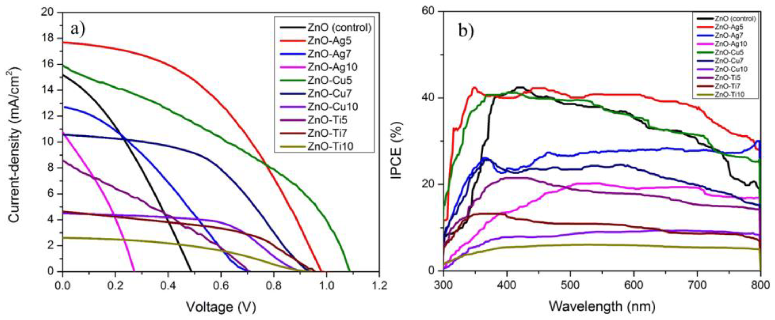
| JSC (mA/cm2) | VOC (V) | FF | PCE (%) | |
|---|---|---|---|---|
| ZnO NFs (control) | 15.08 | 0.49 | 0.33 | 2.41 |
| ZnO-Ag5 | 17.83 | 0.99 | 0.47 | 8.30 |
| ZnO-Ag7 | 12.69 | 0.71 | 0.31 | 2.82 |
| ZnO-Ag10 | 10.90 | 0.27 | 0.31 | 0.93 |
| ZnO-Cu5 | 16.00 | 1.09 | 0.37 | 6.41 |
| ZnO-Cu7 | 10.58 | 0.96 | 0.47 | 4.78 |
| ZnO-Cu10 | 4.53 | 0.92 | 0.54 | 2.27 |
| ZnO-Ti5 | 8.60 | 0.70 | 0.28 | 1.75 |
| ZnO-Ti7 | 4.65 | 0.96 | 0.46 | 2.05 |
| ZnO-Ti10 | 2.61 | 0.94 | 0.40 | 0.98 |
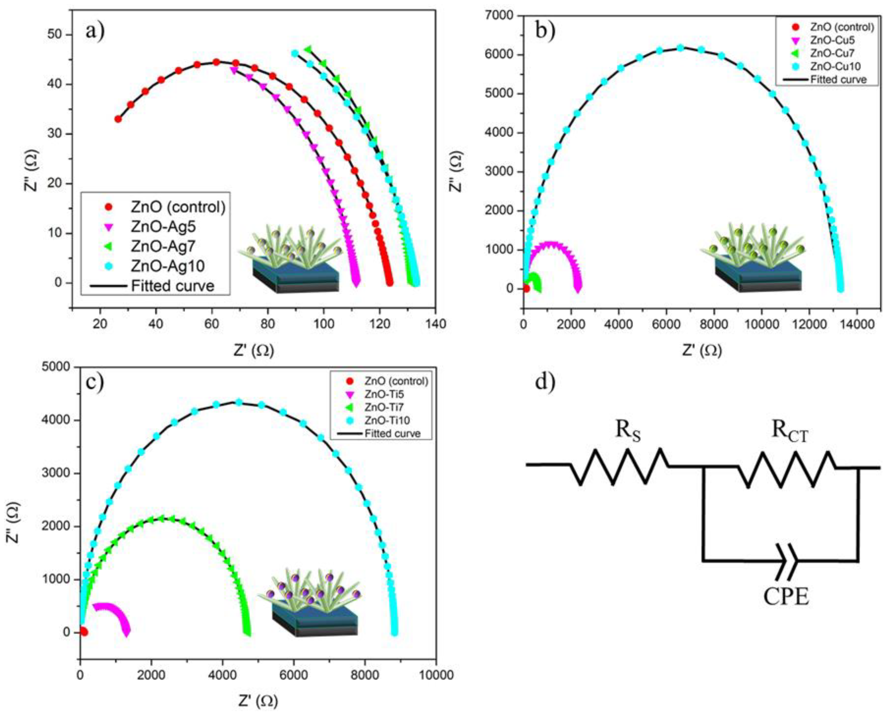
| RS (Ω) | RCT (Ω) | CPE (µF) | n | |
|---|---|---|---|---|
| ZnO NFs (control) | 2.29 × 10⁻¹¹ | 121.38 | 44.0 | 0.805 |
| ZnO-Ag5 | 1.58 × 10⁻¹¹ | 111.61 | 302 | 0.85 |
| ZnO-Ag7 | 7.45 × 10⁻¹² | 131.74 | 156 | 0.86 |
| ZnO-Ag10 | 7.45 × 10⁻¹² | 133.21 | 326 | 0.82 |
| ZnO-Cu5 | 1.57 × 10⁻¹¹ | 2284.4 | 2646 | 0.95 |
| ZnO-Cu7 | 1.13 × 10⁻¹¹ | 637.14 | 1948 | 0.95 |
| ZnO-Cu10 | 21.84 | 13287 | 3190 | 0.95 |
| ZnO-Ti5 | 0.00021 | 1297.1 | 4751 | 0.86 |
| ZnO-Ti7 | 4.05 | 4709.5 | 4462 | 0.94 |
| ZnO-Ti10 | 18.98 | 8811.3 | 2763 | 0.99 |
Publisher’s Note: MDPI stays neutral with regard to jurisdictional claims in published maps and institutional affiliations. |
© 2022 by the authors. Licensee MDPI, Basel, Switzerland. This article is an open access article distributed under the terms and conditions of the Creative Commons Attribution (CC BY) license (https://creativecommons.org/licenses/by/4.0/).
Share and Cite
Mohamed Saheed, M.S.; Mohamed, N.M.; Singh, B.S.M.; Saheed, M.S.M.; Jose, R. Optoelectronic Enhancement of Perovskite Solar Cells through the Incorporation of Plasmonic Particles. Micromachines 2022, 13, 999. https://doi.org/10.3390/mi13070999
Mohamed Saheed MS, Mohamed NM, Singh BSM, Saheed MSM, Jose R. Optoelectronic Enhancement of Perovskite Solar Cells through the Incorporation of Plasmonic Particles. Micromachines. 2022; 13(7):999. https://doi.org/10.3390/mi13070999
Chicago/Turabian StyleMohamed Saheed, Mohamed Salleh, Norani Muti Mohamed, Balbir Singh Mahinder Singh, Mohamed Shuaib Mohamed Saheed, and Rajan Jose. 2022. "Optoelectronic Enhancement of Perovskite Solar Cells through the Incorporation of Plasmonic Particles" Micromachines 13, no. 7: 999. https://doi.org/10.3390/mi13070999
APA StyleMohamed Saheed, M. S., Mohamed, N. M., Singh, B. S. M., Saheed, M. S. M., & Jose, R. (2022). Optoelectronic Enhancement of Perovskite Solar Cells through the Incorporation of Plasmonic Particles. Micromachines, 13(7), 999. https://doi.org/10.3390/mi13070999