Abstract
This paper presents a hybrid waveguide based on metal surface plasmon polaritons (SPPs) at 1550 nm comprising two silver (Ag) nanowires and a rectangular silicon (Si) waveguide. Due to the strong coupling effect observed in both the metal SPP mode and Si waveguide mode, excellent waveguide characteristics, such as a small effective modal area and long transmission length, could be achieved. The research results revealed that the proposed hybrid waveguide could achieve an ultra-long transmission distance of 270 µm and normalized effective mode area of 0.01. Furthermore, the cross-sectional size of the waveguide was 500 nm × 500 nm, which helped in achieving a subwavelength size. In addition, the hybrid waveguide was resistant to manufacturing errors. These excellent performances indicate that the proposed waveguide has great application potential in optoelectronic integrated circuits.
1. Introduction
With the recent advances in the field of optical communications, there has been an increase in the performance requirements of waveguides [1,2,3,4,5]. In particular, there have been rapid advances in optoelectronic integrated systems. These systems require smaller optical devices [6] to improve the system integration. Therefore, the waveguides require both a long transmission distance and small normalized mode area [7,8,9]. In this context, surface plasmon polaritons (SPPs) can be introduced into the waveguide design, which will help in improving the normalized effective mode area of the waveguide [10,11,12], thereby reducing the size of waveguide-based optical devices.
SPPs are caused by the resonance excitation of incident photons with free electron gas on a metal surface [13,14,15,16]. They are widely used for optical manipulation at the subwavelength scale because they can restrict light to a considerably smaller range than the diffraction limit [17,18]. Currently, the most widely used precious metal SPPs are gold (Au) and silver (Ag) [19]. In recent years, several types of waveguides have been designed based on SPPs [20,21,22], and the normalized effective mode area of waveguides has been significantly improved [10,24,25]. However, further research is required to simultaneously ensure a long transmission distance and small normalized effective mode area.
In this study, we developed a long-range hybrid waveguide operating at 1550 nm. The hybrid waveguide is composed of two Ag nanowires and a silicon (Si) waveguide. The waveguide structure has two coupling regions, which strengthens the mode coupling. Due to the strong coupling between the Ag SPPs and Si medium, the hybrid waveguide exhibits both a compact mode area and an extremely long transmission distance. The cross-sectional area of the waveguide is 500 nm × 500 nm, and a subwavelength structure is realized. Moreover, the proposed hybrid waveguide is resistant to manufacturing errors and has a wide range of applications in optical communication systems owing to its advantages.
2. Structure Design
The hybrid waveguide consists of two Ag nanowires and a conventional Si waveguide structure. The entire structure is filled with SiO2 cladding, which acts as a low exponential gap between Si and Ag [23]. Excellent waveguide characteristics were obtained as a result of the double-mode coupling of Ag and Si in this structure.
The 3D structure and cross-section of the proposed hybrid waveguide are shown in Figure 1a,b, respectively. The cross-sectional area of the waveguide was 500 nm × 500 nm. Note that rAg, TSi, and g denote the radius of the Ag nanowire, thickness of the rectangular Si waveguide, and gap height between the Ag nanowire and Si waveguide, respectively.
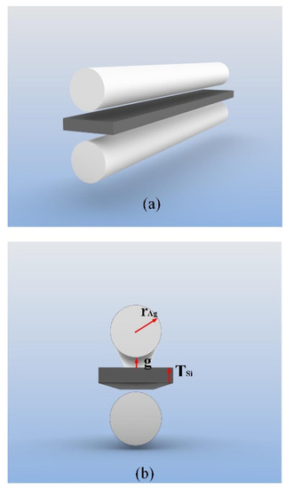
Figure 1.
Structure of the proposed waveguide: (a) 3D layout and (b) cross-section.
3. Methods
The proposed hybrid waveguide utilizes the strong coupling of the Si waveguide and SPP modes to achieve good waveguide performance. It supports an ultra-long transmission distance and has an ultra-compact effective mode area. More importantly, there are two couplings in the hybrid waveguide structure. The superposition of these two couplings resulted in stronger light field localization, which helped improve the waveguide characteristics.
The properties of the hybrid waveguide can be characterized by the following four parameters: Aeff, Lm, FOM, and neff [19,24].
Here, Aeff is the effective modal area; its value determines the optical field constraint capability of the waveguide [25]. A smaller value of Aeff indicates that the light is more localized in the waveguide [26]. Aeff is the ratio of the total electromagnetic energy to the maximum energy density [18]. It is calculated as follows:
where H(r) and E(r) represent the magnetic and electric fields, respectively. In this study, the normalized effective mode area was used; it is calculated using the formula Aeff/A0, where A0 = λ2/4 [27].
Note that Lm represents the transmission length of the hybrid waveguide, and it is defined as follows [28]:
where Neff denotes the effective modal index of the waveguide. Note that Aeff and Lm represent two mutually restrictive parameters, and a smaller effective modal area is often accompanied by a shorter transmission length. FOM is the quality factor of the waveguide, which is a tradeoff between Aeff and Lm. FOM is calculated using the following equation:
where Neff represents the loss of light in the waveguide, and neff represents the real part of Neff, which can be defined as follows:
neff = Re(Neff)
4. Results and Discussion
The hybrid waveguide utilizes the mode coupling of the Si photon and Ag nanowire plasma modes, thereby achieving excellent waveguide characteristics. Strong mode coupling can be obtained easily by adjusting the key structural parameters of the hybrid waveguide, including g, rAg, and TSi.
COMSOL Multiphysics software was used for the numerical analysis of the parameters described in the methods section. In the following simulations, the incident wavelength was 1550 nm, and the relative dielectric constants of Ag, Si, and SiO2 were −129 + 3.3i, 12.25, and 2.25 [18], respectively. In this study, the classical control variable method was adopted to obtain the relationship between the waveguide characteristics and parameters to optimize the waveguide characteristics.
First, the relationship between the waveguide characteristics and g was studied. Herein, g had a range of 1–20 nm. To ensure effective mode coupling and moderate transmission loss, rAg and TSi were fixed at 30 and 20 nm, respectively.
As illustrated in Figure 2, with an increase in g, the normalized effective mode area, transmission length, and neff increased, whereas FOM decreased. The main reason for these results is that the coupling of the hybrid mode weakened with increasing g. The weakened mode coupling resulted in reduced light localization and an increase in the effective mode area. In turn, the length of the light transmission increased. The proposed hybrid waveguide had an extremely long transmission length (Lm: 180–270 µm) while maintaining a very small normalized effective mode area (Aeff/A0: 0.01–0.05). FOM is a compromise between the effective mode area and transmission length. From its calculation formula, it can be observed that the FOM and transmission length exhibit the same change trend, and the proposed hybrid waveguide has a very high-quality factor (FOM: 1350–2000).
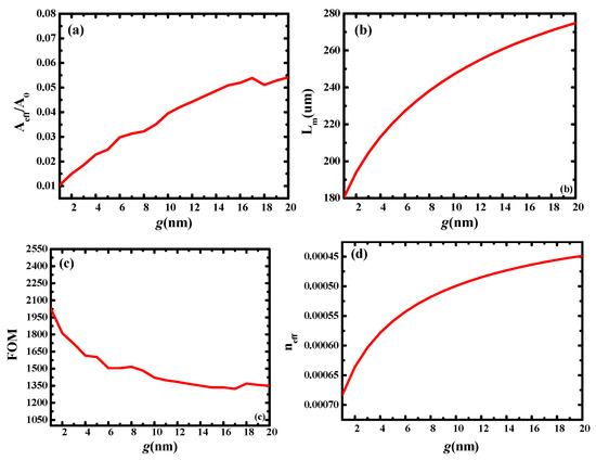
Figure 2.
Dependence of waveguide characteristics on gap height (g): (a) normalized mode area (Aeff/A0); (b) propagation length (Lm); (c) quality factor of waveguide (FOM); and (d) modal effective index (neff).
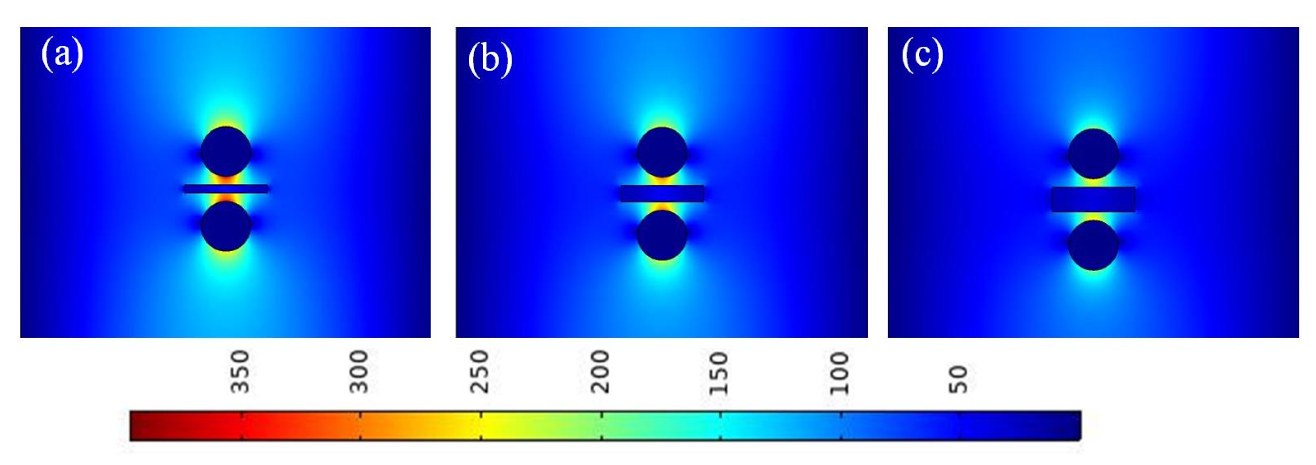
To further verify the abovementioned calculation results, the electric field distributions of the waveguide at different gap heights (i.e., different values of g) are presented. As shown in Figure 3, with an increase in g, the electric field distribution was increasingly diffused. The electric field was most concentrated at g = 5 nm, and it was concentrated in the gap region. As g increased, the electric field gradually spread beyond the gap region. This result is consistent with that shown in Figure 2. In this study, considering the characteristics of the waveguide and the actual manufacturing process, a value of 10 nm was selected for g in the following simulations.
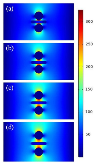
Figure 3.
Electric field distributions of waveguide at different gap heights (g): (a) g = 5 nm; (b) g = 10 nm; (c) g = 15 nm; and (d) g = 20 nm.
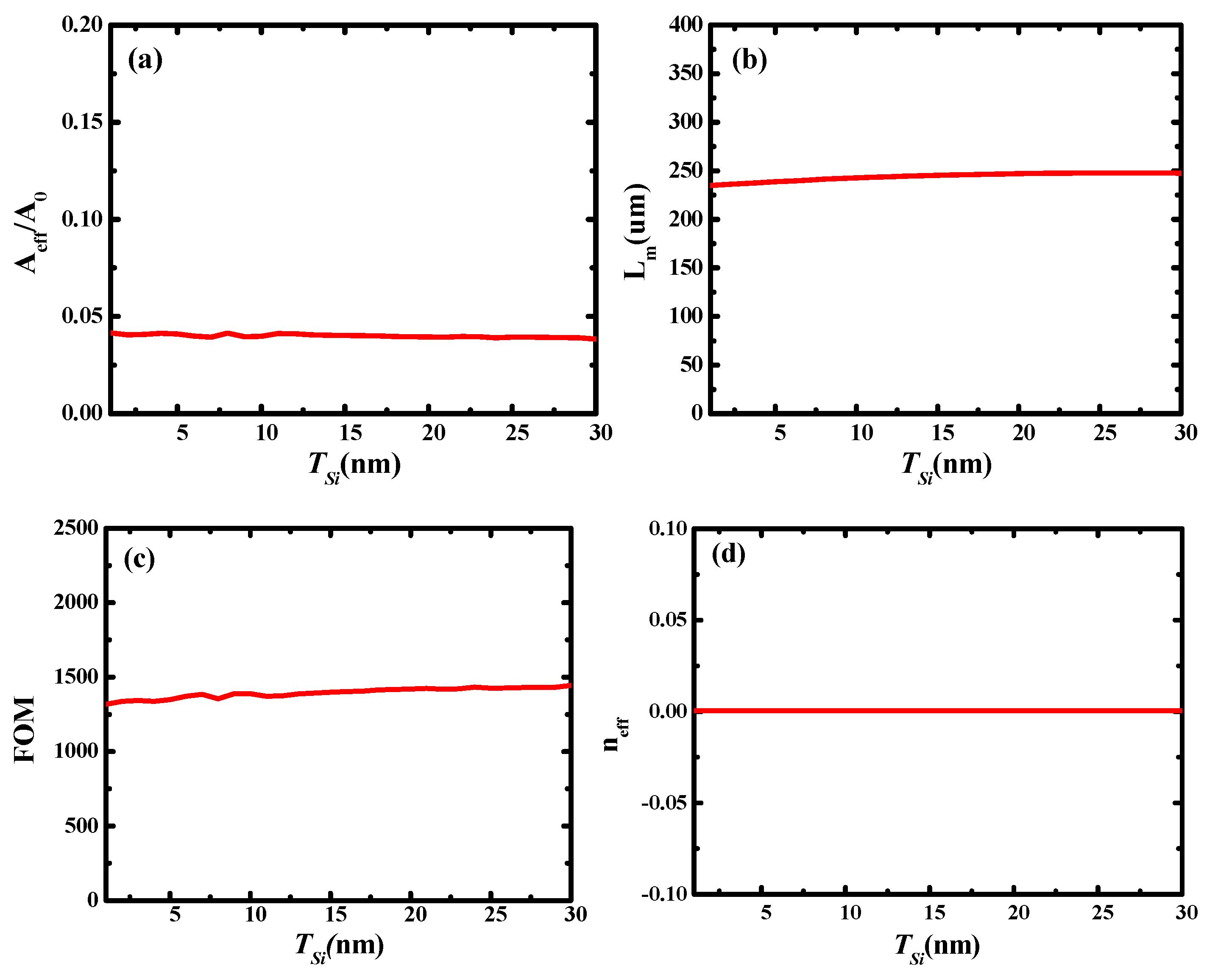
Subsequently, the influence of different Si thicknesses (i.e., different values of TSi) on the waveguide characteristics was investigated. In this calculation, the value of TSi varied in the range of 1–30 nm, rAg was 30 nm, and g was 10 nm. The results are shown in Figure 4, wherein, it can be observed that the characteristics of the hybrid waveguide were only slightly affected by the Si thickness because it had no effect on the coupling of the two hybrid modes.

Figure 4.
Dependence of waveguide characteristics on Si thickness (TSi): (a) normalized mode area (Aeff/A0); (b) propagation length (Lm); (c) quality factor of waveguide (FOM); and (d) modal effective index (neff).
To verify the above conclusions, the electric field distributions for different Si thicknesses were obtained. Here, Figure 5a–c show the electric field distributions at different values of TSi. It can be observed that for different Si thicknesses, the electric field of the waveguide did not diffuse, and the light was well localized. This is consistent with the calculation results shown in Figure 4. Therefore, we fixed TSi at 20 nm in the following simulations.

Figure 5.
Electric field distributions at different Si thicknesses (TSi): (a) TSi = 10 nm; (b) TSi = 20 nm; and (c) TSi = 30 nm.
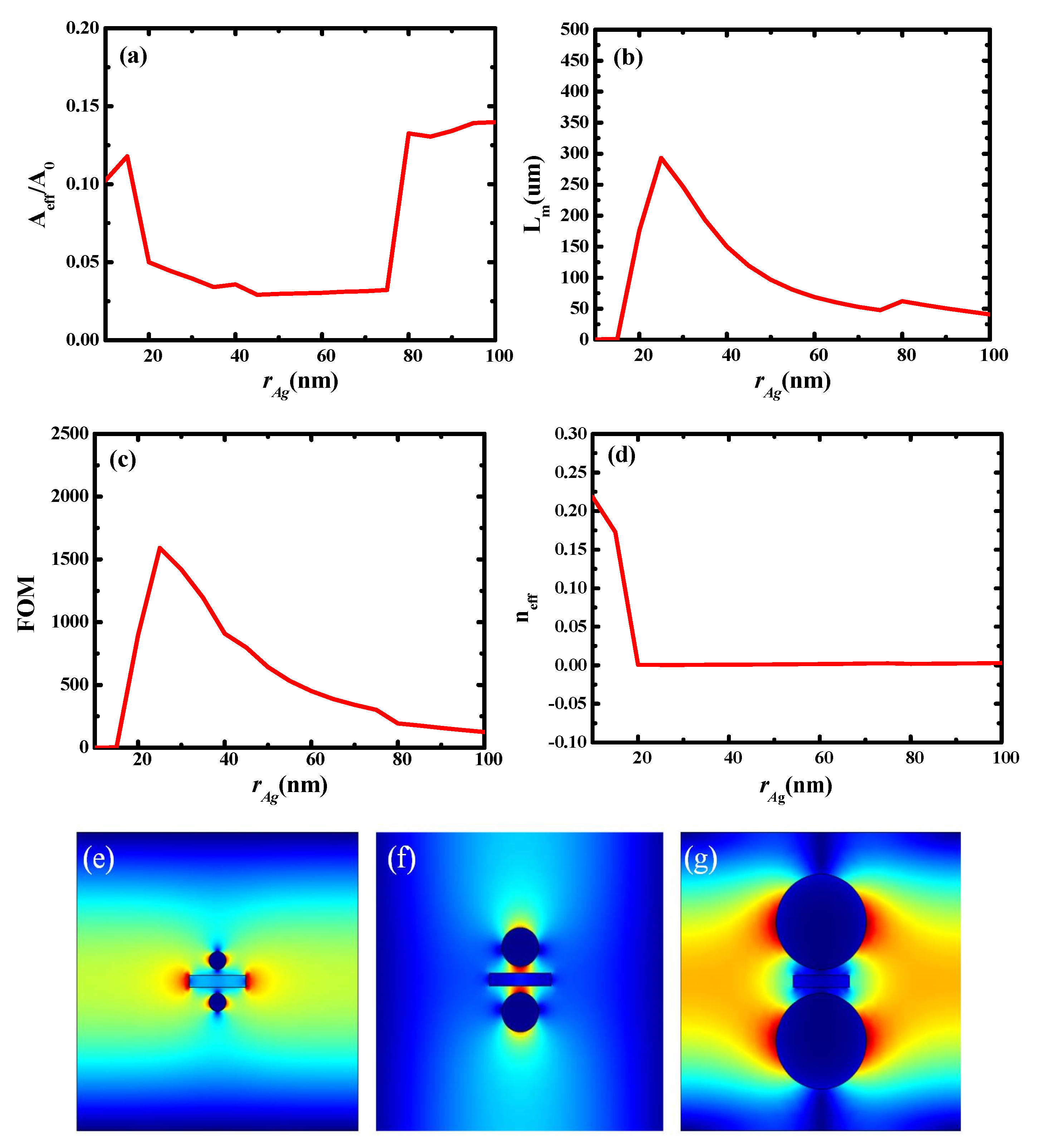
Subsequently, the effect of the radius of the Ag nanowires (rAg) on the waveguide characteristics was explored. Here, rAg had a range of 10–100 nm, and g and TSi were fixed at 10 and 20 nm, respectively. Figure 6a–d show the dependence of Aeff/A0, Lm, FOM, and neff on rAg, respectively. It can be observed that the effective mode area (Aeff/A0) was very large, and the transmission distance (Lm) was short in the region where rAg was less than 20 nm and rAg was greater than 75 nm. The primary reason for this phenomenon is that no mode coupling occurred in this region. Furthermore, the waveguide exhibited good characteristics when rAg was in the range of 20–75 nm. This is due to the strong mode coupling occurring in this region.
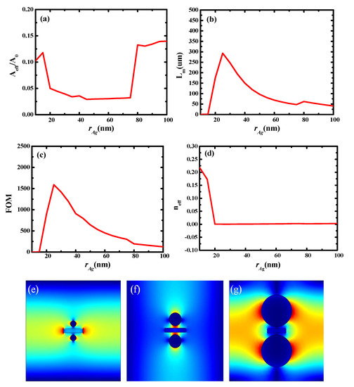
Figure 6.
Dependence of waveguide characteristics on radius of Ag nanowires (rAg): (a) normalized mode area (Aeff/A0); (b) propagation length (Lm); (c) quality factor of waveguide (FOM); (d) modal effective index (neff); (e) electric field distributions at rAg = 15 nm; (f) electric field distributions at rAg = 30 nm; and (g) electric field distributions at rAg = 80 nm.
Here, Figure 6e–g show the electric field distributions at rAg = 15, 30, and 80 nm, respectively. It can be observed that at rAg = 15 and 80 nm, no coupling occurred, and the electric field was dispersed in the cladding, whereas at rAg = 30 nm, mode coupling occurred, and the electric field was concentrated in the gap region. This is consistent with the calculation results shown in Figure 6a–d.
Figure 7 shows the electric field distributions at different values of rAg (20–70 nm). As rAg increased, the electric field became more localized because a larger radius of the Ag nanowires leads to stronger mode coupling. Considering this observation in combination with the results observed in Figure 6, a value of 30 nm was selected for rAg in the following simulations.
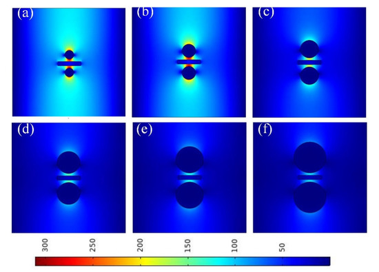
Figure 7.
Electric field distributions at different values of rAg: (a) rAg = 20 nm; (b) rAg = 30 nm; (c) rAg = 40 nm; (d) rAg = 50 nm; (e) rAg = 60 nm; and (f) rAg = 70 nm.
Based on the aforementioned results, it can be concluded that the characteristics of the waveguide can be optimized by adjusting the geometric parameters. Thus, the proposed hybrid waveguide exhibited a small effective mode area and an ultra-long transmission distance.
5. Fabrication Processing and Fabrication Error Tolerance
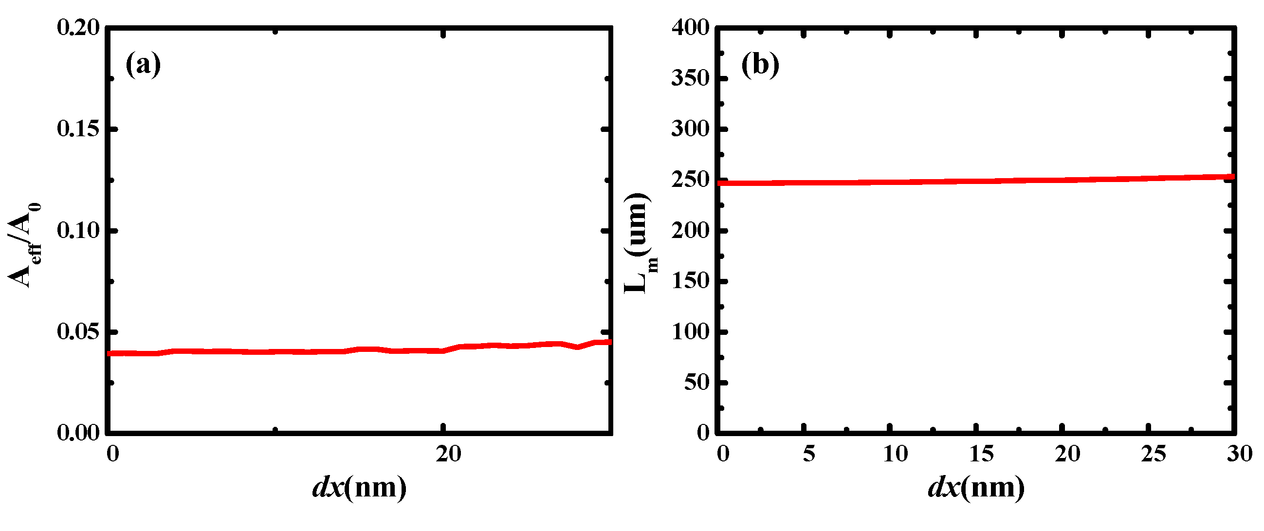
After all the geometric parameters were determined, a hybrid waveguide was fabricated using the standard micromachining process [29,30]. All the geometric parameters of the waveguide could be precisely controlled, except for the central symmetry of the two Ag nanowires. Next, we investigated the difference in waveguide characteristics caused by the deviation of the center position of the two Ag nanowires (dx). In this simulation, g, rAg, and TSi were 10, 30, and 20 nm, respectively. As shown in Figure 8, the center asymmetry error, dx (1–30 nm), caused errors of only 7% and 2.4% for Aeff/A0 and Lm, respectively.
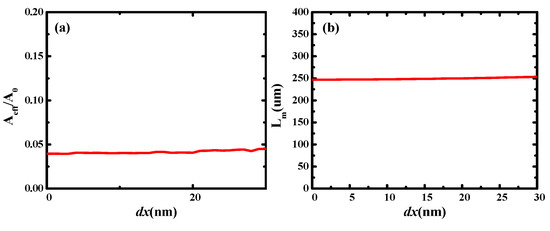
Figure 8.
Dependence of waveguide properties on central symmetric error (dx): (a) normalized mode area (Aeff/A0); (b) propagation length (Lm); (c) quality factor of waveguide (FOM); and (d) modal effective index (neff).
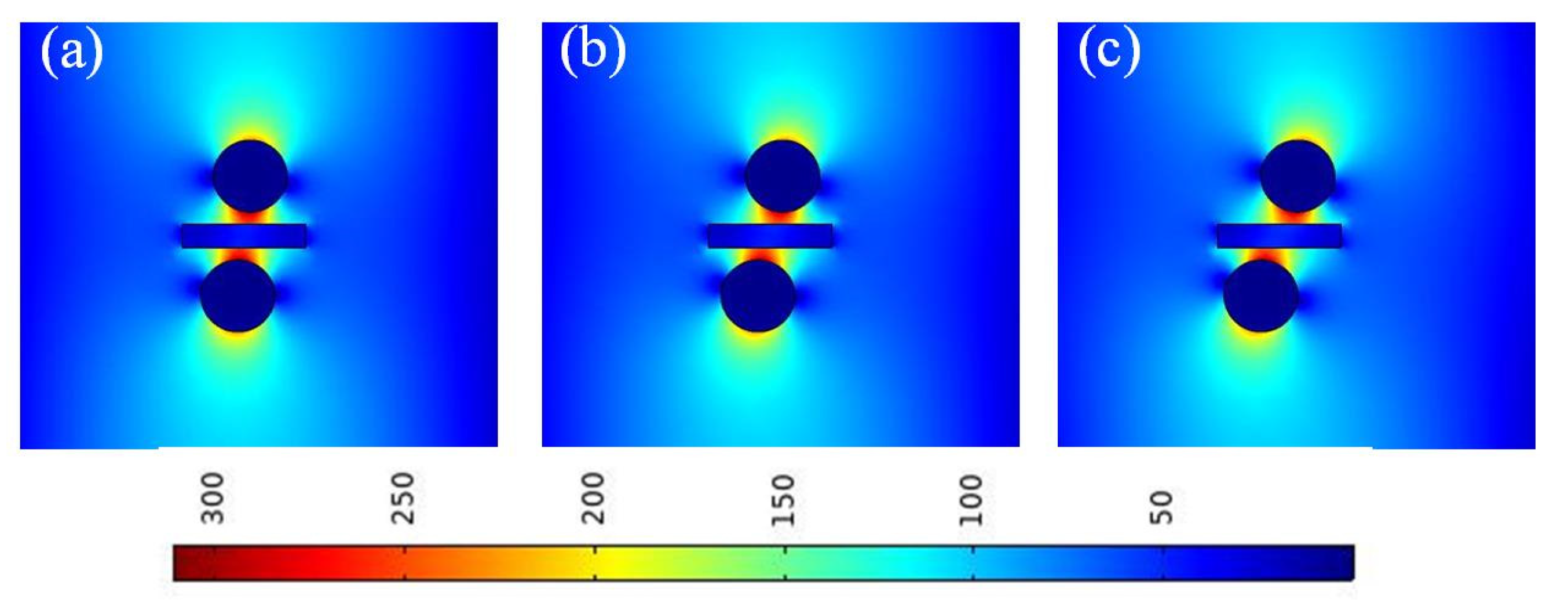
Figure 9 shows the electric field distributions at different values of dx (10, 20, and 30 nm). As dx increased, the waveguide maintained strong mode coupling and good electric field localization, which is consistent with the results observed in Figure 8. These results showed that the hybrid waveguide is reliable and robust against manufacturing errors.

Figure 9.
Electric field distributions at different values for dx: (a) dx = 10 nm; (b) dx = 20 nm; and (c) dx = 30 nm.
6. Conclusions
In this study, a hybrid waveguide based on metal SPPs and operating at 1550 nm was proposed. The hybrid waveguide achieved both a small effective modal area and long transmission length using the strong coupling between the metal SPP mode and Si waveguide mode. The results showed that the waveguide achieved an ultra-long transmission distance of 270 µm and effective mode area of 0.01. The cross-sectional size of the waveguide was only 500 nm × 500 nm, which realized a subwavelength size. The results showed that the properties of the proposed waveguide are resistant to manufacturing errors. These excellent performances indicate that the proposed waveguide has great application potential in optoelectronic integrated circuits.
Author Contributions
Y.W. wrote the main manuscript text and performed the simulations and calculations. H.L. and S.W. gave the constructive suggestion. Other authors edited the manuscript. All authors have read and agreed to the published version of the manuscript.
Funding
This research was funded by the National Natural Science Foundation of China (Grant No. U1866212).
Institutional Review Board Statement
Not applicable.
Informed Consent Statement
Not applicable.
Data Availability Statement
Not applicable.
Acknowledgments
We would like to thank Qu Sheng and Dong Lu for their precious advice in this paper.
Conflicts of Interest
The authors declare no conflict of interest.
References
- Ferreira, P.; Almeida, G.; Mendona, C.R. A simple strategy for increasing optical waveguide performance using spherical aberration. Opt. Laser Technol. 2021, 142, 107235. [Google Scholar] [CrossRef]
- Chandra, V.; Ranjan, R. Performance analysis of different slot waveguide structures for evanescent field based gas sensor applications. Opt. Quantum Electron. 2021, 53, 1–5. [Google Scholar] [CrossRef]
- Arianfard, H.; Wu, J.; Juodkazis, S.; Moss, D.J. High Performance Optical Filters Using Three Waveguide Coupled Sagnac Loop Reflectors. arXiv 2021, arXiv:2103.07822. [Google Scholar]
- Oulton, R.F.; Sorger, V.J.; Genov, D.A.; Pile, D.F.P.; Zhang, X. A hybrid plasmonic waveguide for subwavelength confinement and long-range propagation. Nat. Photonics 2008, 2, 496–500. [Google Scholar] [CrossRef] [Green Version]
- Dai, D.; He, S. A silicon-based hybrid plasmonic waveguide with a metal cap for a nano-scale light confinement. Opt. Express 2009, 17, 16646–16653. [Google Scholar] [CrossRef] [PubMed]
- Chan, S.J. Automated inspection systems for the electronics industry: As IC devices get smaller and smaller, the challenge of detecting faults becomes bigger and bigger. EE-Eval. Eng. 2005, 44, 56–59. [Google Scholar]
- Hu, Y.-J.; Xu, L.; Zhang, Q.; Yuan, C.-W.; Liu, J.-L.; Sun, Y.-F. A compact high-power microwave TM01-TE01 mode converter. Rev. Sci. Inst. 2021, 92, 094703. [Google Scholar] [CrossRef] [PubMed]
- Rui, X.; Jian, S. The Graphene Square Waveguide with Small Normalized Mode Area. IEEE Photonics Technol. Lett. 2017, 29, 1643–1646. [Google Scholar]
- Singh, R.; Priye, V. Si3N4—SiO2 Based Curve Slot Waveguide for High Confinement Factor and Low Mode Effective Area along with Biosensing Application. Silicon 2021, 14, 859–867. [Google Scholar] [CrossRef]
- He, X.; Liu, F.; Lin, F.; Shi, W. Tunable 3D Dirac-semimetals supported mid-IR hybrid plasmonic waveguides. Opt. Lett. 2021, 46, 472–475. [Google Scholar] [CrossRef]
- Teng, D.; Wang, K.; Huan, Q.; Chen, W.; Li, Z. High-performance light transmission based on graphene plasmonic waveguides. J. Mater. Chem. C 2020, 8, 6832–6838. [Google Scholar] [CrossRef]
- Teng, D.; Wang, K. Theoretical Analysis of Terahertz Dielectric–Loaded Graphene Waveguide. Nanomaterials 2021, 11, 210. [Google Scholar] [CrossRef] [PubMed]
- Cuevas, M.; Depine, R.A. Excitation of surface plasmon polaritons along the sinusoidal boundary of a metamaterial. Phys. Rev. B Condens. Matter 2008, 78, 125412. [Google Scholar] [CrossRef] [Green Version]
- Tgab, C.; Erb, D. Propagation of surface plasmon polaritons at the interface of metal-free metamaterial with anisotropic semiconductor inclusions. Optik 2022, 254, 168678. [Google Scholar]
- Wang, Y.; Liu, H.; Wang, S.; Cai, M.; Ma, L. Optical Transport Properties of Graphene Surface Plasmon Polaritons in Mid-Infrared Band. Crystals 2019, 9, 354. [Google Scholar] [CrossRef] [Green Version]
- Teng, D.; Wang, Z.; Huan, Q.; Wang, H.; Wang, K. A low loss platform for subwavelength terahertz graphene plasmon propagation. Opt. Mater. 2022, 128, 112436. [Google Scholar] [CrossRef]
- Wang, Y.; Wang, S.; Cai, M.; Liu, H. A Long Propagation Distance Hybrid Triangular Prism Waveguide for Ultradeep Subwavelength Confinement. IEEE Sens. J. 2019, 19, 11159–11166. [Google Scholar] [CrossRef]
- Lu, D.; Liu, H.; Wang, S.; Sheng, Q.; Lei, W. Hybrid Tube-Triangle Plasmonic Waveguide for Ultradeep Subwavelength Confinement. J. Lightwave Technol. 2017, 35, 2259–2265. [Google Scholar]
- Bian, Y.; Ren, Q.; Kang, L.; Yue, T.; Werner, P.L.; Werner, D.H. Deep-subwavelength light transmission in hybrid nanowire-loaded silicon nano-rib waveguides. Photonics Res. 2018, 6, 37–45. [Google Scholar] [CrossRef] [Green Version]
- Zhou, T.; Gou, X.; Xu, W.; Li, Y.; Zhai, X.; Li, H.; Wang, L. Dynamically Tunable Plasmon-induced Transparency in a T-shaped Cavity Waveguide Based on Bulk Dirac Semimetals. Plasmonics 2021, 16, 323–332. [Google Scholar] [CrossRef]
- Qiao, Q.; Xu, Y.; Zhang, L.; Li, W.; Shi, Z. Spoof surface plasmon polariton waveguide with spiral structure units. Eur. Phys. J. Plus 2021, 136, 874. [Google Scholar] [CrossRef]
- Teng, D.; Wang, K.; Li, Z. Graphene-Coated Nanowire Waveguides and Their Applications. Nanomaterials 2020, 10, 229. [Google Scholar] [CrossRef] [PubMed] [Green Version]
- Huang, J. Terahertz graphene modulator based on hybrid plasmonic waveguide. Phys. Scr. 2021, 96, 125525. [Google Scholar] [CrossRef]
- Ma, Y.; Farrell, G.; Semenova, Y.; Wu, Q. Hybrid nanowedge plasmonic waveguide for low loss propagation with ultra-deep-subwavelength mode confinement. Opt. Lett. 2014, 39, 973–976. [Google Scholar] [CrossRef]
- Dan, X.; Huang, Y.; Wang, X.; Hao, H.; He, H. Hybrid Surface Plasmon Polariton Waveguide of Low-Loss and Ultra-Small Modal Area. Acta Opt. Sin. 2015, 35, 0623003. [Google Scholar] [CrossRef]
- Ma, Z.A.; Zhang, P.B.; Li, L.; Ni, X.A. Endless single-polarization single-mode photonic-crystal planar waveguide arrays with ultra-large mode area and ultra-low transmission loss—ScienceDirect. Optik 2021, 238, 166474. [Google Scholar] [CrossRef]
- Kumar, S.; Kumar, P.; Ranjan, R. A Metal-Cap Wedge Shape Hybrid Plasmonic Waveguide for Nano-Scale Light Confinement and Long Propagation Range. Plasmonics 2021, 17, 95–105. [Google Scholar] [CrossRef]
- Wang, Y.; Liu, H.; Wang, S.; Cai, M. A waveguide-integrated graphene-based subwavelength electro-optic switch at 1550 nm. Opt. Commun. 2021, 495, 127121. [Google Scholar] [CrossRef]
- Tilmans, H.; Baert, K.; Verbist, A.; Puers, R. CMOS foundry-based micromachining. J. Micromech. Microeng. 1996, 6, 122. [Google Scholar] [CrossRef]
- Mohammad, T.; He, S.; Mrad, R.B. Conventional surface micromachining process for the fabrication of a linear optical phased array based on piston micromirrors. J. Micromech. Microeng. 2021, 31, 065009. [Google Scholar] [CrossRef]


Publisher’s Note: MDPI stays neutral with regard to jurisdictional claims in published maps and institutional affiliations. |
© 2022 by the authors. Licensee MDPI, Basel, Switzerland. This article is an open access article distributed under the terms and conditions of the Creative Commons Attribution (CC BY) license (https://creativecommons.org/licenses/by/4.0/).