Article

Design and Fabrication of Silicon-Blazed Gratings for Near-Infrared Scanning Grating Micromirror

1
Key Laboratory of Optoelectronic Technology and System of the Education Ministry of China, Chongqing University, Chongqing 400030, China
2
National Key Laboratory of Fundamental Science of Novel Micro/Nano Device and System Technology, Chongqing University, Chongqing 400030, China
3
Chongqing Chuanyi Automation Co., Ltd., Chongqing 401121, China
*
Author to whom correspondence should be addressed.
Micromachines 2022, 13(7), 1000; https://doi.org/10.3390/mi13071000
Submission received: 9 May 2022 / Revised: 17 June 2022 / Accepted: 20 June 2022 / Published: 25 June 2022
(This article belongs to the Special Issue Advanced Micro- and Nano-Manufacturing Technologies)

Abstract

:
Blazed gratings are the critical dispersion elements in spectral analysis instruments, whose performance depends on structural parameters and topography of the grating groove. In this paper, high diffraction efficiency silicon-blazed grating working at 800–2500 nm has been designed and fabricated. By diffraction theory analysis and simulation optimization based on the accurate boundary integral equation method, the blaze angle and grating constant are determined to be 8.8° and 4 μm, respectively. The diffraction efficiency is greater than 33.23% in the spectral range of 800–2500 nm and reach the maximum value of 85.62% at the blaze wavelength of 1180 nm. The effect of platform and fillet on diffraction efficiency is analyzed, and the formation rule and elimination method of the platform are studied. The blazed gratings are fabricated by anisotropic wet etching process using tilted (111) silicon substrate. The platform is minished by controlling etching time and oxidation sharpening process. The fillet radius of the fabricated grating is 50 nm, the blaze angle is 7.4°, and the surface roughness is 0.477 nm. Finally, the blazed grating is integrated in scanning micromirror to form scanning grating micromirror by MEMS fabrication technology, which can realize both optical splitting and scanning. The testing results show that the scanning grating micromirror has high diffraction efficiency in the spectral range of 810–2500 nm for the potential near-infrared spectrometer application.

1. Introduction

Diffraction gratings are widely used as core optical splitters in modern optical devices such as ultra-precision measurement systems [1,2], spectrometers [3,4,5,6], semiconductor lasers [7,8], display techniques [9,10], and so on. With the development of micro-electro-mechanical system (MEMS) technology, there are kinds of silicon diffraction gratings developed, including rectangle gratings, sine gratings, and blazed gratings. Particularly, the blazed gratings exhibit excellent optical characteristics since they can focus the major part of the incident energy on a single non-zero diffraction order, which is beneficial for spectral analysis and detection. Generally, the diffraction and spectral characteristics of the blazed gratings are primarily dependent on the shape of the grating grooves, such as blaze angle and the topography of the grating groove. Therefore, it is important to design a proper blaze angle in a certain spectral range and control the grating shape during fabrication. For example, Zamkotsian et al. designed blazed gratings with a blaze angle of 5.04° working at the spectral range of 400–800 nm for high throughput spectrographs in space missions [11]. Sokolov et al. proposed blazed gratings with a blaze angle of 0.6°, 0.8°, and 1.0°, respectively, to achieve high diffraction efficiency at the tender X-ray region [12].
Mechanical ruling technique [12,13,14,15,16], ion beam etching (IBE) technique [17,18,19,20,21,22], and anisotropic wet etching technique [23,24,25] are commonly used to fabricate silicon-blazed gratings. Mechanical ruling technique using a specific shape diamond cutting tool extrudes on the grating substrate coated with aluminum or gold film to form grating grooves, which is simple and low-cost. But this method is not suitable for batch manufacturing of large area grating due to its low efficiency. Moreover, it is not compatible with MEMS fabrication process, and it is difficult to fabricate gratings on movable MEMS devices. During the IBE process, the grating structure is shaped through physical sputtering of materials. The blazed gratings with different blaze angle can be fabricated by adjusting the incident angle of ion beam, the duty cycle of the photoresist mask, and the etching rate ratio of the photoresist to the substrate material, which has the advantages of good direction, speed and shape control, high precision and smooth grating surface can be achieved [17,18]. Nevertheless, the fabrication process depends on the IBE equipment, so it is complex and costly. Furthermore, the etching rate of IBE is very low, and it is also not suitable for batch preparation of gratings. Anisotropic wet etching is the most promising technique for fabrication of high-performance blazed grating. It is a simple and convenient method to realize arbitrary blazed angle by using tilted (111) silicon wafers. Moreover, it provides atomically smooth blazed facets since it is formed by (111) lattice plane. However, there is always a small platform or nub left on the top of grating groove after etching, which will lead to amounts of stray light and reduce the diffraction efficiency. Voronov et al. fabricated 6° tilted blazed facets grating grooves by KOH solution, but there were silicon nubs on its top [26]. So, they used piranha solution (H2SO4 + H2O2) to chemically oxidize the silicon nubs, and then sharpened the gratings by hydrofluoric acid (HF) removal of the resulting oxides. However, there were 26 cycles applied to remove the 25-nm wide nubs in total, leading to complex fabrication process and large surface roughness. Fr u ¨ hauf and Kr o ¨ nert prepared triangular grating grooves with 500 nm width platform by anisotropic wet etching process using tetramethylammonium hydroxide (TMAH) solution [27], then the grating grooves were etched for a short time by isotropic etching (mixed solution of HNO3, HF, and CH3COOH). Finally, the radius of the convex edge was diminished to 50 nm, but the surface of the triangular gratings was relatively rough. Miles et al. fabricated a master blazed grating with platform width of 30 nm by combining electron beam etching and anisotropic wet etching [28]. To maximize the diffraction efficiency, the master grating was replicated using UV nanoimprinting lithography with the result that the platform became a flat trough which was small enough to be shadowed by the neighboring facet. However, gratings made on the imprint resist are limited in applications compared with those made on the silicon substrate. In our previous work, an 800–1800 nm blazed grating whose blaze angle is 7.4° was prepared by anisotropic wet etching and oxidation sharpening, but the width of the platform was 540 nm and there was a lack of systematic optimization research on etching and sharpening process [29].
The purpose of this paper is to design and fabricate high performance silicon-blazed gratings for near-infrared scanning grating micromirror used in miniature spectrometers. First, the blazed grating working at wavelength range from 800 nm to 2500 nm was designed. Effect of platform and fillet on diffraction efficiency is simulated and optimized. Reactive ion etching (RIE) and wet isotropic etching are investigated to prepare SiO2 mask and narrow its width. The grating groove is formed by anisotropic wet etching of tilted (111) silicon substrate, and then sharpened by high temperature oxidation sharpening process. The optimal anisotropic wet etching time and oxidation sharpening time was obtained, and the grating grooves were analyzed by optical profiler, scanning electron microscope (SEM), and atomic force microscope (AFM). Finally, the blazed grating is integrated in scanning micromirror by MEMS fabrication technology to form scanning grating micromirror, and the optical properties are tested by diffraction efficiency measurement system and diffracted wavelength range test system.

2. Design of the Grating Structure
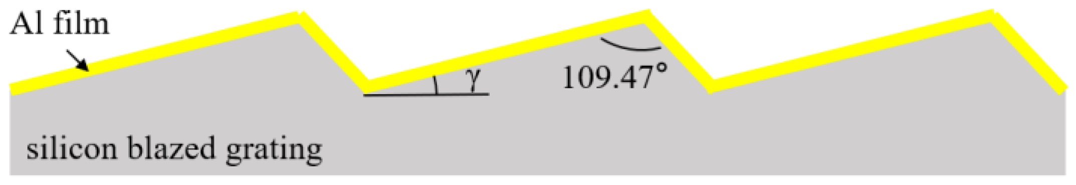
Performance of the blazed grating is quite dependent on its groove parameters, including blaze angle and grating constant. In this section, based on diffraction theory and diffraction efficiency simulation, the blazed grating structure is determined.

2.1. Principles

Blazed grating exhibits excellent optical characteristics because it can concentrate light energy at a specific diffraction order through diffraction plane at a specific blaze angle. The blazed grating and the optical path of its diffraction are depicted in Figure 1.
The monochromatic light obliquely incident on the blazed grating, and then it is diffracted into discrete directions. Each grating profile can be considered to be a small, slit-shaped source of diffracted light that combines to form a set of diffracted wave fronts. Because the diffracted lights from different grating surfaces have the same phase, thus resulting in constructive interference. The relationships of incident angle α, diffraction angle β, grating constant d and the incident light wavelength λ are given by the diffraction grating equation, as shown in Equation (1):
d sin α sin β = m λ
where m is the diffraction order. When the light is blazing at +1 diffraction order, a relationship between the incident, diffraction, and blaze angle γ can be extracted as Equation (2):
α γ = β + γ
Then substituting Equation (2) into Equation (1), the relationship between wavelength, grating constant, incident angle, and blaze angle is expressed by Equation (3).
γ = 1 2 α arcsin sin α λ d
It is seen that the wavelength of the grating is closely related to blaze angle and grating constant. Moreover, a spectrum will be generated at +1 diffraction order if a polychromatic light incident on the blazed grating in the same way, and any wavelength λ in the spectrum must satisfy the grating equation. Substituting sin β ≥ −1 into Equation (2), the reasonable range of grating constant is obtained by Equation (4),
d λ max 1 + sin α
where λmax denotes the maximum wavelength in the spectrum.
As the blazed grating is applied in the miniature near-infrared spectrometer whose spectrum range is from 800 nm to 2500 nm. The incident angle α is fixed at 14.1° as the requirement of optical path in the spectrometer. According to Equation (4), grating constant must satisfy d ≥ 2 μm. However, a large grating constant will result in a low spectral resolution. Therefore, considering the spectral range, spectral resolution, and lithography resolution, the grating constant is determined to be 4 μm. The blaze wavelength is derived from the thumb rule that the diffraction efficiency drops to 50% of its peak value at 2/3 λb and at 9/5 λb, where λb is the blaze wavelength [30]. The wide spectrum ranges from 800 nm to 2500 nm should contain the range from 2/3 λb to 9/5 λb to get high diffraction efficiency. So, the blaze wavelength is calculated as 1200–1389 nm. Substituting it into Equation (3), the desired blaze angle is 8.7°–10.0°.

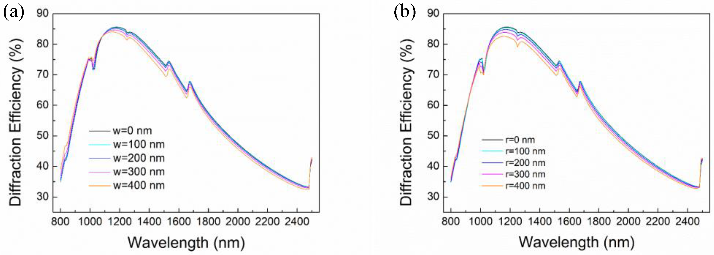
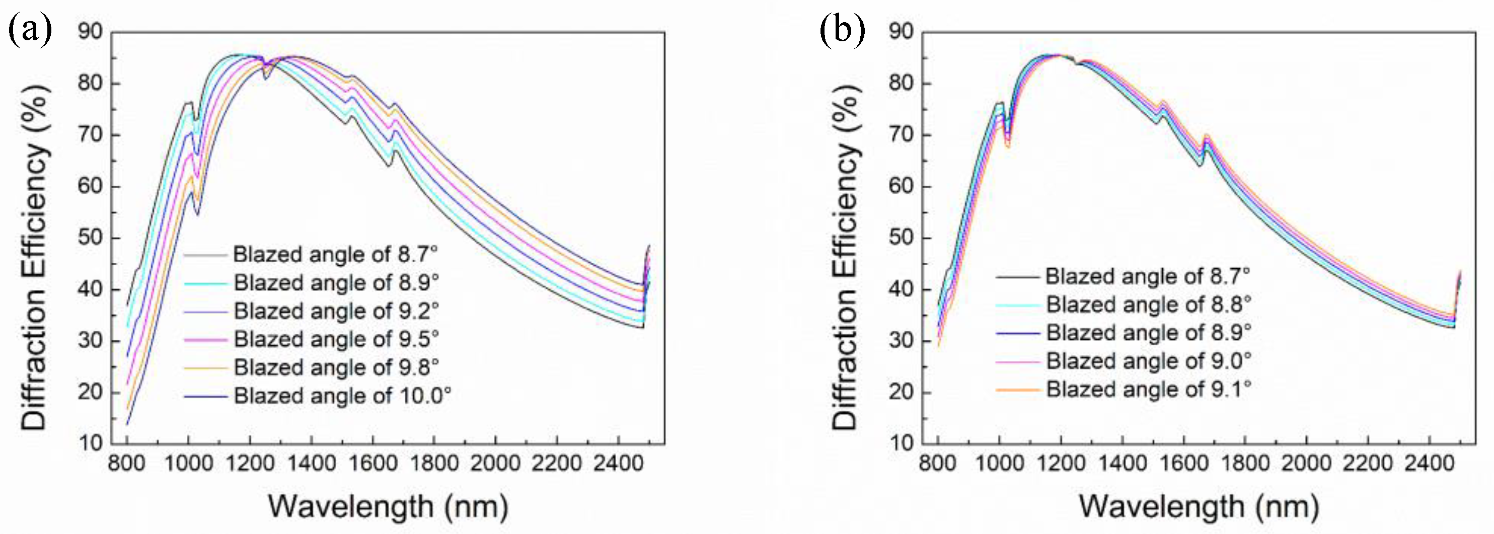
2.2. Optimization of the Blaze Angle

PCGrate is the software used for the exact calculation of diffraction efficiency by the accurate boundary integral equation method. In this work, the diffraction efficiency curves under different blaze angles are simulated using PCGrate Demo v.6.4 to get optimal blaze angle. Figure 2 shows the grating model for simulation. The gray area is the planar silicon-blazed grating with grating constant of 4 μm. To increase reflectivity, a 100 nm-thick aluminum (Al) film is added to cover the grating surface. Since the grating is fabricated by anisotropic wet etching process, the grating groove is formed by intersecting (111) faces and the apex angle of the grating is 109.47°. So, the border profile of the grating is defined by the blaze angle.
In order to preliminarily determine the range of optimal blaze angel, diffraction efficiency curves under blaze angle of 8.7°, 8.9°, 9.2°, 9.5°, 9.8°, and 10.0° are analyzed, as shown in Figure 3a. It can be seen that the diffraction efficiency increases rapidly and then decreases slowly as the wavelength increases. It gradually goes down in short wavelength and changes in the opposite direction in long wavelength as the increase of the blaze angle. Moreover, some anomalous jumps are clearly observed on these curves, which can be attributed to the exceeding 90° of the diffraction angle at a high order. The diffraction efficiency jumps into the lower orders when higher orders are diffracted into the grating surface and become evanescent. Through comparative analysis of diffraction efficiency at different blazed angles and different wavelengths, it is found that the blazed grating has higher diffraction efficiency when the blaze angle is 8.9°. The diffraction efficiency is higher than 32.84%. It means that the optimal blaze angle is around 8.9°. Then, the blaze angle is further optimized by setting blaze angle as 8.7°, 8.8°, 8.9°, 9.0°, 9.1° respectively. The diffraction efficiency curves are shown in Figure 3b. It shows that the diffraction efficiency is higher than 33.24% when the blaze angle is 8.8°, so the final optimized blaze angle is 8.8°. At this time, the lowest diffraction efficiency is 33.24% at wavelength 800 nm, while the maximum value is 85.62% at blaze wavelength 1180 nm.
However, a platform or fillet usually remains on the top of the grating groove during the blazed grating fabrication process, which induces stray light and degrades the diffraction efficiency. Therefore, it should be considered in the design process. For a clear view, diffraction efficiency under blaze angle of 8.8° varying with different platform and fillet size are also investigated, as shown in Figure 4. It can be seen that the diffraction efficiency gradually decreases as the platform becomes wider. Assuming the top of the grating is a platform, the diffraction efficiency at blaze wavelength of 1150 nm is 84.03% when the platform width is 400 nm, while it is 85.45% when the platform width is 100 nm. While for fillet, the diffraction efficiency at blaze wavelength is 82.54% and 85.39% respectively, when the radius is 400 nm and 100 nm. The result denotes that the diffraction efficiency indeed decreases with the increase of platform or fillet size, so it needs to be minimized in subsequent fabrication process. Furthermore, the effect of platform or fillet on diffraction efficiency becomes small when the width of the platform or fillet is less than 100 nm. Therefore, the platform width or the fillet radius of the blazed gratings should be sharpened to less than 100 nm to obtain high performance.

3. Fabrication and Characterization of Blazed Gratings

After the determination of the grating structure, it is important to control the groove shape during the next fabrication process. In this section, an improved process is proposed to fabricate the blazed gratings.

3.1. Experimental

To fabricate the sawtooth grating groove, the tilted (111) silicon wafer was used as the substrate. Figure 5a illustrates the schematic diagram of titled silicon wafer cutting. It was cut by (111) silicon ingot, which rotated a certain angle θ from (111) crystal plane to (110) plane along [ 1 ¯ 10] orientation. The cutting angle θ is equal to the designed blaze angle γ. According to the characteristics of anisotropic wet etching, the grating groove was formed by the intersection of slowly etched surface (111) faces, as shown in Figure 5b.
The microfabrication process of the blazed grating is depicted in Figure 6. First, the double sides polished, tilted (111) silicon wafer with cutting angle of 8.8° was used as the substrate (Figure 6a), whose thickness was 500 ± 20 μm, resistivity was 70–80 Ω · cm, and error of the cutting angle is ±0.5°. Then, a 300-nm-thick SiO2 layer was thermally oxidated on the wafer surface (Figure 6b). Next, a photoresist layer was coated on the SiO2 layer and a series of 500-nm-wide photoresist stripes which had 4 μm period and paralleled to the [ 1 ¯ 10] direction was fabricated by stepper lithography (Figure 6c). The SiO2 layer was etched by reactive ion etching (RIE) technique and buffered oxidate etch (BOE) to form etching mask of gratings (Figure 6d). Subsequently, the grating groove was shaped by anisotropic wet etching (Figure 6e). An additional oxidation of gratings without removing the SiO2 etching mask was purposely taken to further decrease the platform on grating top (Figure 6f). The desired grating groove was obtained by removing SiO2 on both sides of the wafer (Figure 6g). Finally, a 100 nm-thick aluminum was deposited on the grating surface using magnetron sputtering to increase the reflectivity for spectral range of 800–2500 nm (Figure 6h).

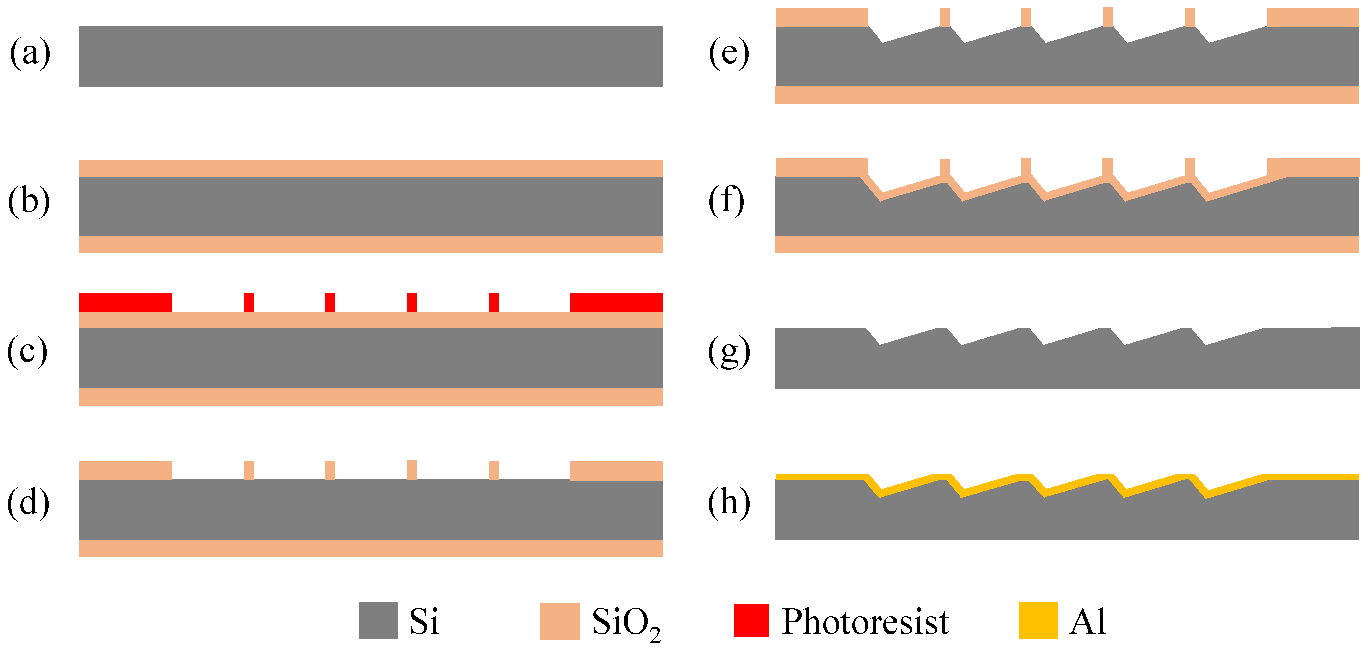
3.2. Fabrication of Grating Etching Mask

SiO2 mask was used as etching mask of gratings in the experiment. In order to reduce the influence of platform on the performance of gratings, the SiO2 mask should be minimized. RIE and BOE isotropic etching was used to fabricate SiO2 mask and reduce its width. Generally, it was difficult to accurately etch 300 nm-thick SiO2 layer and stop on the Si surface only using RIE technique. If the SiO2 layer was overetched, the underlying Si substrate would be also slightly etched, forming a large nub on the top of the grating groove after anisotropic wet etching process, as shown in Figure 7a. The nub was also shaped by (111) plane and hard to be eliminated, so the diffraction efficiency is reduced because of introducing stray light and narrowing the blazed facet. Whereas, long-time wet etching in BOE could damage and cause peeling of the photoresist. Therefore, after RIE etching of SiO2 for 250 nm, BOE was applied to etch the remaining SiO2, and the etching would spontaneously stop at the interface of SiO2 and Si. The grating groove fabricated in this way is shown in Figure 7b, and the nub is successfully avoided.
Optimized parameters of RIE and BOE wet etching were investigated for good etching uniformity and small size etching mask. Sulfur hexafluoride (SF6) was used as the etchant gas, and oxygen (O2) was used as protection gas in the RIE process. A high SF6 flow and high etching power resulted in a high etching rate, which was set to be 30 sccm and 150 W respectively. As the O2 flow increased, anisotropy and uniformity of RIE etching were both improved. However, a small width of SiO2 stripes was needed in the experiment, which can be realized by isotropic lateral etching at low O2 flow. Moreover, high O2 flow would easily remove the photoresist, so O2 flow was set to be 5 sccm. After 180 s of etching by RIE, the thickness of the remaining SiO2 was 50nm, then it was overetched by BOE solution for 90 s. Images of photoresist stripes before etching process and SiO2 stripes after photoresist removing are shown in Figure 8. It could be seen that the width of the grating mask was narrowed from 500 nm to 200 nm.

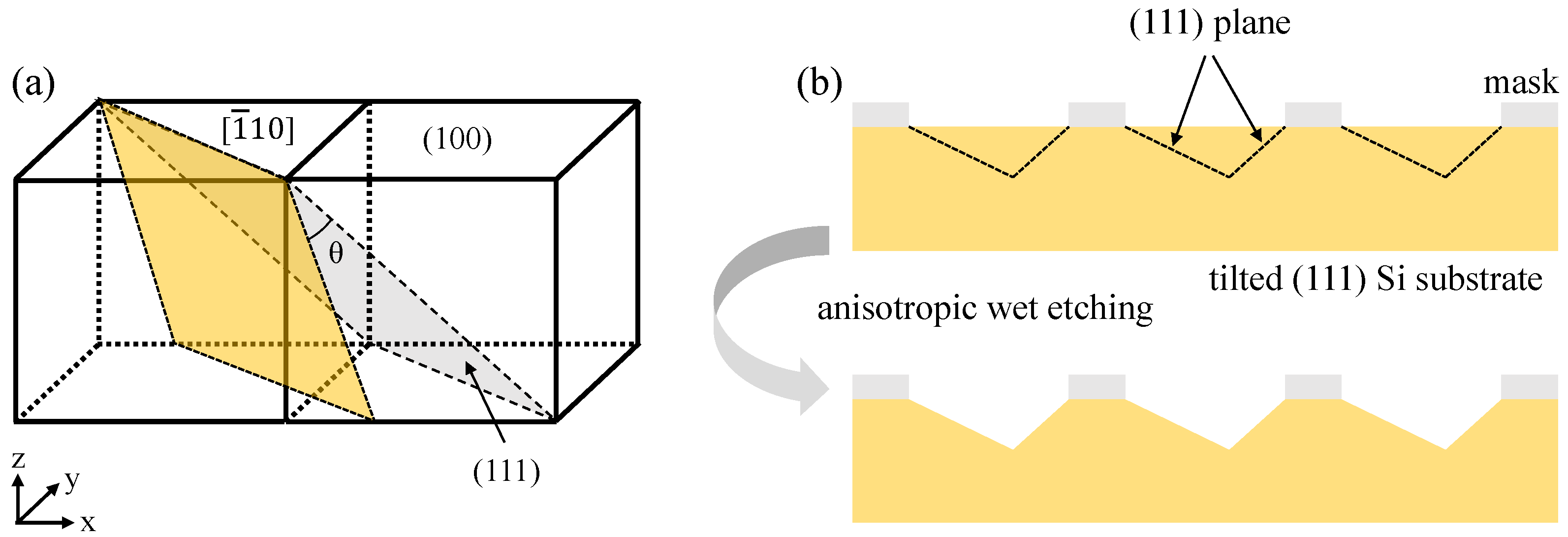
3.3. Anisotropic Wet Etching of Blazed Gratings

The gratings were prepared by anisotropic wet etching process. The exposed silicon was etched in the anisotropic etching solution at different rates according to the crystal direction. When the two (111) crystal planes intersected, the etching stopped, and the triangle blazed gratings were obtained. The blaze angle of the gratings was the tangent angle of tilted silicon wafer. For smooth grating surface, tetramethylammonium hydroxide (TMAH) solution with mass fraction of 25% was used in the experiment. The grating groove shapes at different etching time of 75 s, 3 min, 5 min, and 7 min were observed by scanning electron microscopy (SEM) after SiO2 mask removing, and the morphology of the platform on the top of the grating was analyzed. It was seen that a 165-nm-width platform was formed on the top of the grating due to the protection of a narrow SiO2 mask as the etching time was 75 s, as shown in Figure 9a. The rounded edge was caused by lateral corner cut corrosion. Then, a small nub emerges as the etching time increases, due to the over etching of the (111) planes and shaped by new (111) sidewalls. The height of the nub was 32 nm and the width was 163 nm after 3 min etching, as shown in Figure 9b. The nub became larger in depth and smaller in width with the increasing of etching time because of the constant etching of (111) planes, as shown in Figure 9c,d. When the etching time was 7 min, the width of the nub was 52 nm, and the height was 57 nm. However, the nub was difficult to eliminate further because the SiO2 stripes fell off as continuous etching. Moreover, the long-term wet etching led to an increase in surface roughness of the grating surface, which ultimately affected the diffraction efficiency. Hence, the suitable etching time was 75 s.

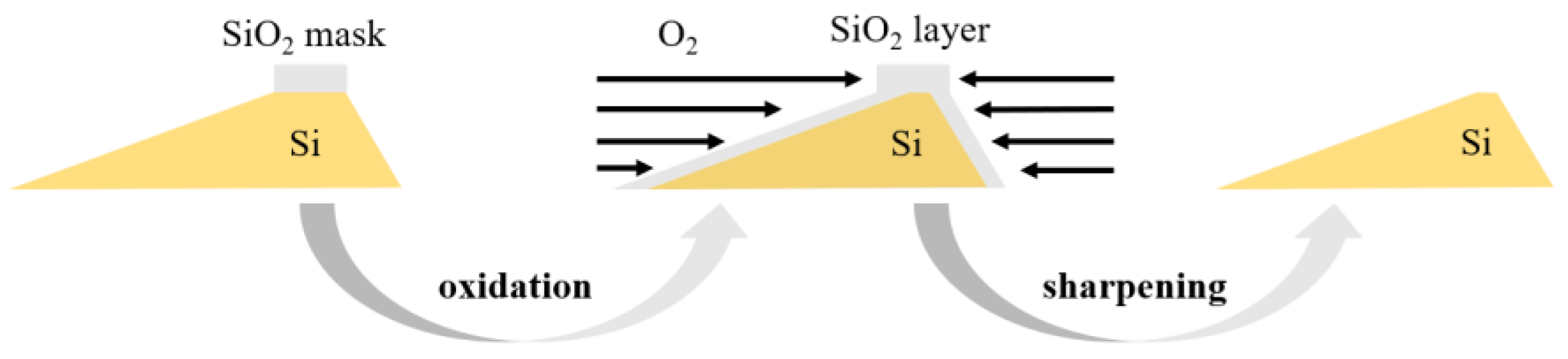
3.4. Oxidation Sharpening

After anisotropic wet etching process, an oxidation sharpening process was subsequently employed to further decrease the platform without removing the SiO2 etching mask. Figure 10 schematically displays the oxidation sharpening process. The grating samples were thermally oxidated for hours at 1050 °C, oxidation rate at the top of the grating groove was much lower than that of the groove sides since the SiO2 mask was served as a barrier layer. As a result, the thermal oxide layers are mainly grown at the sides of the groove. Subsequently, the oxidation layer was etched in BOE solution until the Si surface was hydrophobic, and the grating groove was effectively sharpened.
The grating groove depended on the oxidation time. The grating samples was oxidated at 1050 °C for 1 h, 2 h, and 4 h, respectively, and the SEM images of the gratings after the oxide layer removing are shown in Figure 11. It can be seen that the platforms decreased and finally converted to a fillet. The radius of the fillet first decreased and then increased as the oxidation time increased. There was a 150-nm-wide platform on the grating top when the oxidation time was 1 h. When the oxidation time increased to 2 h, the platform turned to a fillet, whose radius was 50 nm. However, continued oxidation for 4 h caused the fillet to become larger, and the radius was about 130 nm. Therefore, the optimized oxidation sharpening time was 2 h.
The grating profile measured by the optical profiler is shown in Figure 12a. The actual blaze angle was 7.4°, which had an offset of 1.4° to the designed value. This deviation mainly came from two sources. One was the cutting angle error of the tilted (111) substrate, another was the etching time difference between upper and lower surfaces. The atomic force microscopy (AFM) image of the blazed grating is also presented in Figure 12b. It could be seen that the measured root mean square (RMS) roughness of the grating surface with aluminum reflective coating was 0.477 nm, that proved the grating surface possessed great smoothness.

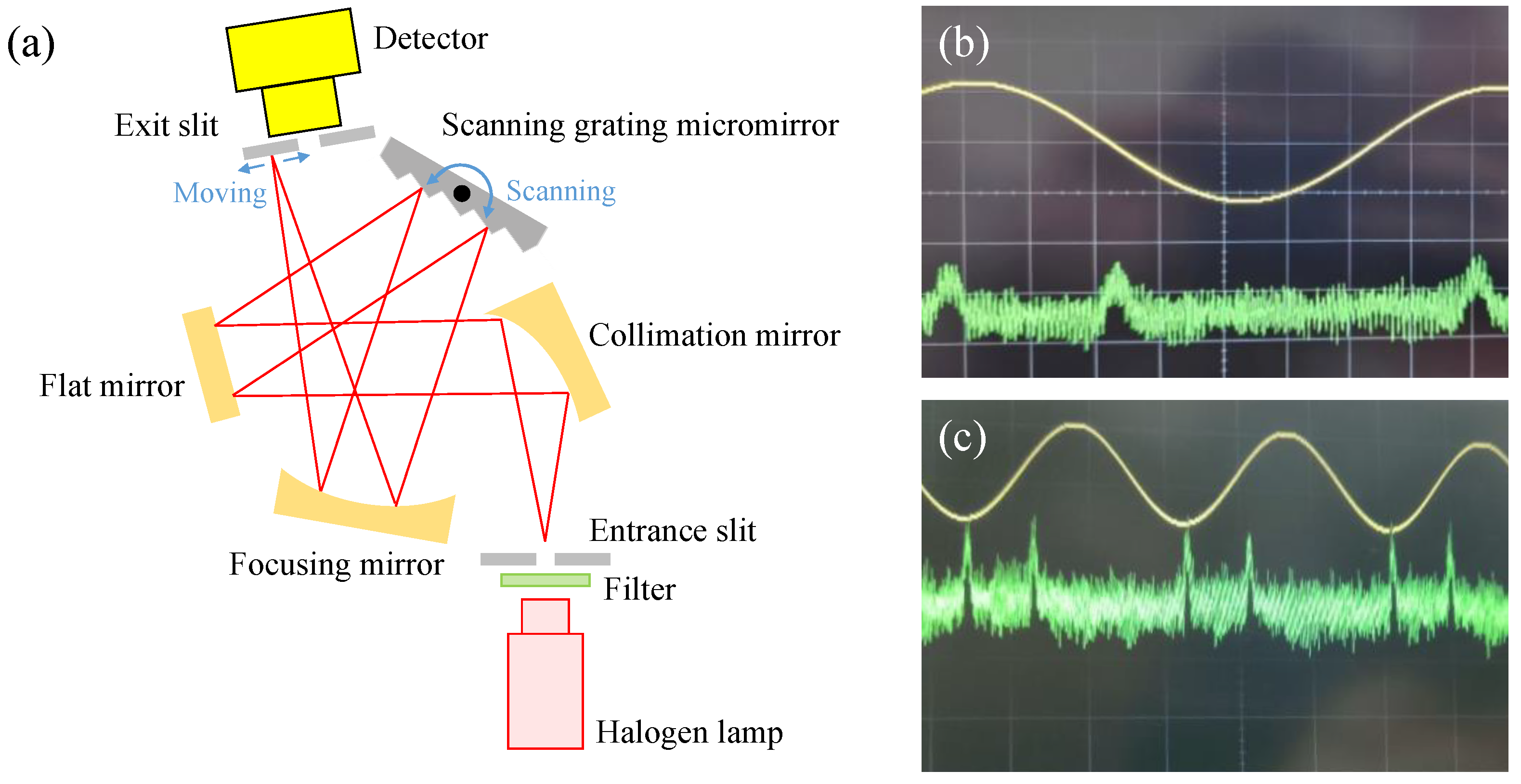
4. Application in Scanning Grating Micromirror

The fabricated blazed grating was integrated on the movable micromirror to form a scanning grating micromirror applying in the miniature near-infrared spectrometer. It could realize optical splitting and scanning at the same time. The schematic diagram of the scanning grating micromirror is shown in Figure 13. A compound light dispersed into lights arranging in order of wavelength to form a spectrum by the dispersion role of the integrated blazed grating. With the micromirror rotating around torsional springs, the incident angle continuously changed as well as the diffraction angle, resulting in scanning of the diffracted lights. Consequently, a single detector at a fixed position could be able to detect the diffraction spectrum. Applying this device in the near-infrared spectrometer can avoid using expensive near-infrared detection array and reduce the spectrometer size. Using standard MEMS fabrication technology, the blazed grating was integrated on the backside of the scanning micromirror to form scanning grating micromirror. The fabricated device is shown in Figure 13b,c.
The absolute diffraction efficiency is an important performance parameter for the scanning grating micromirror, which indicates the optical energy transfer capability. It is a measure of how much optical power is diffracted into a designated direction compared to the power incident onto the diffractive element, which is defined as:
η λ , m = I λ , m I λ
where Iλ,m is diffraction light power at diffraction order of m, and Iλ is the incident light power. Figure 14a schematically showed the measurement for absolute diffraction efficiency. The set up mainly consisted of a laser device, an optical power meter, and a scanning grating micromirror. First, the laser was normally incident into the optical power meter to directly detect the incident laser power Iλ. Then, the laser was incident into the center of the scanning grating micromirror with the incident angle of 14.1°, and the optical power meter was moved to detect the light power at +1 diffraction order Iλ+1. According to Equation (5), the absolute diffraction efficiency could be calculated. Figure 14b shows the photographic image of the measurement set up.
Since the laser emitted TM-polarized wave in our test system, the measured results indicated as diffraction efficiency under TM polarization. Here, theoretical diffraction efficiency of blazed grating with blaze angle of 7.4° under TM polarization was obtained by PCGrate, and the theoretical values at given wavelength spots are given in Table 1. The actual diffraction efficiency was tested and compared to its corresponding theoretical value. The results showed high diffraction efficiency of the blazed grating but an error of 4–5% to the ideal value. This error was derived from the oxidation of Al reflective layer and dust adhesion on the grating surface in the test environment, which was acceptable.
The diffracted wavelength range of the proposed scanning grating micromirror was tested with our previous NIR spectrometer setup [31]. As Figure 15a demonstrates, the light was emitted through a filter and an entrance slit. Then it was collimated by an off-axis parabolic mirror and reflected toward the scanning grating micromirror by using a flat mirror. The diffracted lights were reflected and focused on the detector’s plane through an exit slit. As the scanning grating micromirror tilted, the diffraction lights with varying wavelengths were scanned through the detector which gave the spectrum information for the incoming lights.
During the diffracted wavelength range measurement, a set of narrow band filters and a halogen tungsten lamp were used. The detector’s response over scanning process was amplified and recorded with an oscilloscope. The measured data with 810 nm (bandwidth of 10 nm) and 2580 nm (bandwidth of 50 nm) filters are given in Figure 15b and c respectively. The yellow line is the driving voltage for the rotation of scanning grating micromirror, and the green line is the spectral signal received by the detector. Two peaks of detected signal per period of driving voltage are observed since the diffracted light scans through the detector back and forth in a rotation period of scanning grating micromirror. The peaks on the recorded detector’s response (the green line) indicates that the proposed scanning grating micromirror has enough diffraction efficiency in the spectral range of 810–2500 nm for potential spectrometer application.

5. Conclusions

In this paper, a blazed grating applied in near-infrared scanning grating micromirror was designed, fabricated, and characterized. Based on the diffraction theory and diffraction efficiency simulation, the blaze angle and grating constant were determined as 8.8° and 4 μm, respectively. The effects of the platform and fillet on the diffraction efficiency were also investigated, showing a larger platform and fillet resulted in lower diffraction efficiency. However, the diffraction efficiency hardly decreased when the platform width or the fillet radius was less than 100 nm, which provided a target for controlling the defects on grating shapes in the fabrication process. By optimizing RIE and wet etching process, the SiO2 mask width was narrowed from 500 nm to 200 nm. The blazed grating was fabricated by anisotropic wet etching combined with high temperature oxidation sharpening process using tilted (111) silicon substrate. The platform was minished to a fillet with radius of 50 nm by optimizing etching time and oxidation sharpening time. The grating grooves were analyzed by optical profiler and AFM, showing the fabricated blaze angle was 7.4° and the RMS roughness of the grating surface with aluminum reflective coating was 0.477 nm. Finally, the blazed grating was integrated in scanning micromirror to form scanning grating micromirror using MEMS fabrication technology, which can realize both optical splitting and scanning. The testing results show that the scanning grating micromirror has high diffraction efficiency in the spectral range of 810–2500 nm. The proposed design and fabrication method of blazed gratings are promising to obtain high-performance blazed gratings applied in spectral analysis instruments.

Author Contributions

S.Z. and D.L. designed and fabricated the blazed grating. Y.Z. gave suggestions on grating design and test. Q.W. designed the scanning grating micromirror and its test system. S.Z. and H.Z. completed the optical performance measurement of the scanning grating micromirror. S.Z. and D.L. wrote and revised the paper. All authors have read and agreed to the published version of the manuscript.

Funding

This work was supported by the National Key R&D Program of China (Grant No. 2018YFF01011200) and the National Natural Science Foundation of China (Grant No. 61804016).

Institutional Review Board Statement

Not applicable.

Informed Consent Statement

Not applicable.

Data Availability Statement

Data available on request due to restrictions, e.g., privacy or ethical. The data and material presented in this study are available on request from the corresponding author.

Conflicts of Interest

The authors declare no conflict of interest.

References

  1. Chen, F.; Brown, G.M.; Song, M.M. Overview of 3-D shape measurement using optical methods. Opt. Eng. 2000, 39, 10–22. [Google Scholar]
  2. Sansoni, G.; Patrioli, A. Noncontact 3D sensing of free-form complex surfaces. Proc. SPIE 2001, 4309, 232–239. [Google Scholar]
  3. Lin, D.M.; Fan, P.Y.; Hasman, E.; Brongersma, M.L. Dielectric gradient metasurface optical elements. Science 2014, 345, 298–302. [Google Scholar] [CrossRef] [PubMed]
  4. Zhao, B.S.; Meijer, G.; Schöllkopf, W. Quantum reflection of He2 several nanometers above a grating surface. Science 2011, 331, 892–894. [Google Scholar] [CrossRef] [PubMed]
  5. Xing, J.Y.; Cui, H.; Hu, P.H.; Jin, S.Q.; Hu, M.Y.; Xia, G.; Hu, H.B. Gratings in dispersion-compensated polarization Sagnac interferometer. Opt. Commun. 2020, 458, 124806. [Google Scholar] [CrossRef]
  6. Sandfuchs, O.; Kraus, M.; Brunner, R. Structured metal double-blazed dispersion grating for broadband spectral efficiency achromatization. J. Opt. Soc. Am. A 2020, 37, 1369–1380. [Google Scholar] [CrossRef] [PubMed]
  7. Cheng, F.M.; Zhang, J.C.; Wang, D.B.; Gu, Z.H.; Zhuo, N.; Zhai, S.Q.; Wang, L.J.; Liu, J.Q.; Liu, S.M.; Liu, F.Q.; et al. Demonstration of high-power and stable single-mode in a quantum cascade laser using buried sampled grating. Nanoscale Res. Lett. 2019, 14, 123. [Google Scholar] [CrossRef] [Green Version]
  8. Yang, K.; Liu, Y.G.; Wang, Z.; Li, G.Y.; Han, Y.; Zhang, H.W.; Yu, J. Five-wavelength-switchable all-fiber erbium-doped laser based on few-mode tilted fiber Bragg grating. Opt. Laser Technol. 2018, 108, 273–278. [Google Scholar] [CrossRef]
  9. Wang, X.; Wilson, D.; Muller, R.; Maker, P.; Psaltis, D. Liquid-crystal blazed-grating beam deflector. Appl. Opt. 2000, 39, 6545–6555. [Google Scholar] [CrossRef] [Green Version]
  10. Zhou, F.; Hua, J.Y.; Shi, J.C.; Qiao, W.; Chen, L.S. Pixelated blazed gratings for high brightness multiview holographic 3D display. IEEE Photonics Technol. Lett. 2020, 32, 283–286. [Google Scholar] [CrossRef]
  11. Zamkotsian, F.; Zhurminsky, I.; Lanzoni, P.; Tchoubaklian, N.; Schneider, C.; Fricke, S.; Schnieper, M.; Lütolf, F.; Luitot, C.; Costes, V. Convex blazed gratings for high throughput spectrographs in space missions. Proc. SPIE 2019, 11180, 1118051. [Google Scholar]
  12. Sokolov, A.; Huang, Q.S.; Senf, F.; Feng, J.T.; Lemke, S.; Alimov, S.; Knedel, J.; Zeschke, T.; Kutz, O.; Seliger, T.; et al. Optimized highly efficient multilayer-coated blazed gratings for the tender X-ray region. Opt. Express 2019, 27, 16833–16846. [Google Scholar] [CrossRef] [PubMed]
  13. Wood, R.W. The echelette grating for the infra-red. Philos. Mag. 1910, 20, 770–778. [Google Scholar] [CrossRef]
  14. Xu, D.; Owen, J.D.; Papa, J.C.; Reimer, J.; Suleski, T.J.; Troutman, J.R.; Davies, M.A.; Thompson, K.P.; Rolland, J.P. Design, fabrication, and testing of convex reflective diffraction gratings. Opt. Express. 2017, 25, 15252–15268. [Google Scholar] [CrossRef]
  15. Siewert, F.; Lochel, B.; Buchheim, J.; Eggenstein, F.; Firsov, A.; Gwalt, G.; Kutz, O.; Lemke, S.; Nelles, B.; Rudolph, I.; et al. Grating for synchrotron and FEL beamlines: A project for the manufacture of ultra-precise gratings at Helmholtz Zentrum Berlin. J. Synchrotron. Radiat. 2018, 25, 91–99. [Google Scholar] [CrossRef] [Green Version]
  16. Montesanti, R.C.; Little, S.L.; Kuzmenko, P.J.; Bixler, J.V.; Jackson, J.L.; Lown, J.G.; Priest, R.E.; Yoxall, B.E. Strategies for single-point diamond machining a large format germanium blazed immersion grating. Proc. SPIE. 2016, 9912, 991233. [Google Scholar]
  17. Kowalski, M.P.; Cruddace, R.G.; Heidemann, K.F.; Lenke, R.; Kierey, H.; Barbee, T.W.; Hunter, W.R. Record high extreme-ultraviolet efficiency at near-normal incidence from a multilayer-coated polymer-overcoated blazed ion-etched holographic grating. Opt. Lett. 2004, 29, 2914–2916. [Google Scholar] [CrossRef]
  18. Kowalski, M.P.; Cruddace, R.G.; Barbee, T.W.; Hunter, W.R.; Heidemann, K.F.; Nelles, B.; Lenke, R.; Kierey, H. High-efficiency multilayer-coated polymer-overcoated blazed ion-etched holographic gratings for high-resolution EUV astronomical spectroscopy. Proc. SPIE 2004, 5488, 910–921. [Google Scholar]
  19. Fu, Y.; Bryan, N.K.A.; Zhou, W. Self-organized formation of a blazed-grating-like structure on Si (100) induced by focused ion-beam scanning. Opt. Express 2004, 12, 227–233. [Google Scholar] [CrossRef]
  20. Shen, C.; Tan, X.; Jiao, Q.B.; Zhang, W.; Wu, N.; Bayan, H.; Qi, X.D. Convex blazed grating of high diffraction efficiency fabricated by swing ion-beam etching method. Opt. Express 2018, 26, 25381–25398. [Google Scholar] [CrossRef]
  21. Lin, H.; Li, L.F. Fabrication of extreme-ultraviolet blazed gratings by use of direct argon-oxygen ion-beam etching through a rectangular photoresist mask. Appl. Opt. 2008, 47, 6212–6218. [Google Scholar] [CrossRef] [PubMed]
  22. Lin, H.; Zhang, L.C.; Li, L.F.; Jin, C.S.; Zhou, H.J.; Huo, T.L. High-efficiency multilayer-coated ion-beam-etched blazed grating in the extreme-ultraviolet wavelength region. Opt. Lett. 2008, 33, 485–487. [Google Scholar] [CrossRef] [PubMed] [Green Version]
  23. Fujii, Y.; Aoyama, K.; Minowa, J. Optical demultiplexer using a silicon echelette grating. IEEE J. Quantum Electron. 1980, 16, 165–169. [Google Scholar] [CrossRef]
  24. Philippe, P.; Valette, S.; Mata Mendez, O.; Maystre, D. Wavelength demultiplexer: Using echelette gratings on silicon substrate. Appl. Opt. 1985, 24, 1006–1011. [Google Scholar] [CrossRef] [PubMed]
  25. Voronov, D.L.; Lum, P.; Naulleau, P.; Gullikson, E.M.; Fedorov, A.V.; Padmore, H.A. X-ray diffraction gratings: Precise control of ultra-low blaze angle via anisotropic wet etching. Appl. Phys. Lett. 2016, 109, 43112. [Google Scholar] [CrossRef] [Green Version]
  26. Voronov, D.L.; Ahn, M.; Anderson, E.H.; Cambie, R.; Chang, C.H.; Gullikson, E.M.; Heilmann, R.K.; Salmassi, F.; Schattenburg, M.L.; Warwick, T.; et al. High-efficiency 5000 lines/mm multilayer-coated blazed grating for extreme ultraviolet wavelengths. Opt. Lett. 2010, 35, 2615–2617. [Google Scholar] [CrossRef] [Green Version]
  27. Frühauf, J.; Krönert, S. Wet etching of silicon gratings with triangular profiles. Microsyst. Technol. 2005, 11, 1287–1291. [Google Scholar] [CrossRef]
  28. Miles, D.M.; McCoy, J.A.; McEntaffer, R.L.; Eichfeld, C.M.; Lavallee, G.; Labella, M.; Drawl, W.; Liu, B.; DeRoo, C.T.; Steiner, T. Fabrication and diffraction efficiency of a large-format, replicated X-ray reflection grating. Astrophys. J. 2018, 869, 95. [Google Scholar] [CrossRef]
  29. Nie, Q.Y.; Xie, Y.Y.; Chang, F. MEMS blazed gratings fabricated using anisotropic etching and oxidation sharpening. AIP Adv. 2020, 10, 65216. [Google Scholar] [CrossRef]
  30. Mouroulis, P.; Wilson, D.W.; Maker, P.D.; Muller, R.E. Convex grating types for concentric imaging spectrometers. Appl. Opt. 1998, 37, 7200–7208. [Google Scholar] [CrossRef]
  31. Huang, L.K.; Wen, Q.; Huang, J.; Yu, F.; Lei, H.J.; Wen, Z.Y. Miniature broadband NIR spectrometer based on FR4 electromagnetic scanning micro-grating. Micromachines 2020, 11, 393. [Google Scholar] [CrossRef] [Green Version]
Figure 1. Schematic and optical path diffraction of a blazed grating.
Micromachines 13 01000 g001
Figure 2. The grating model for diffraction efficiency simulation.
Micromachines 13 01000 g002
Figure 3. Diffraction efficiency of blazed gratings with blaze angle of (a) 8.7°, 8.9°, 9.2°, 9.5°, 9.8°, and 10.0°; (b) 8.7°, 8.8°, 8.9°, 9.0°, and 9.1°.
Micromachines 13 01000 g003
Figure 4. Diffraction efficiency with different (a) width of platforms; (b) radius of fillets.
Micromachines 13 01000 g004
Figure 5. (a) The schematic diagram of tilted (111) silicon cutting; (b) formation of blazed grating groove by anisotropic wet etching.
Micromachines 13 01000 g005
Figure 6. The fabrication flow of the blazed grating. (a) substrate preparation; (b) thermal oxidation of the substrate; (c) photoresist mask preparation; (d) SiO2 mask preparation; (e) anisotropic wet etching; (f) thermal oxidation of the grating; (g) SiO2 removing; (h) aluminum film deposition.
Micromachines 13 01000 g006
Figure 7. Grating grooves prepared under different grating mask preparation process. (a) only using RIE technique; (b) combining RIE technique and BOE wet etching technique.
Micromachines 13 01000 g007
Figure 8. Images of (a) photoresist stripes before the etching process; (b) SiO2 stripes after photoresist removing.
Micromachines 13 01000 g008
Figure 9. Grating grooves etched by different time. (a) 75 s; (b) 3 min; (c) 5 min; and (d) 7 min.
Micromachines 13 01000 g009
Figure 10. Schematic diagram of oxidation sharpening process.
Micromachines 13 01000 g010
Figure 11. Grating grooves prepared under different oxidation time of (a) 1 h; (b) 2 h; and (c) 4 h.
Micromachines 13 01000 g011
Figure 12. (a) Image of blazed grating profile; (b) AFM image of the blazed grating.
Micromachines 13 01000 g012
Figure 13. (a) Schematic diagram of the scanning grating micromirror; (b) frontside of fabricated scanning grating micromirror chip with actuated coils; (c) backside of fabricated scanning grating micromirror chip integrated with blazed gratings.
Micromachines 13 01000 g013
Figure 14. (a) Schematic diagram and (b) photography of the grating diffraction efficiency measurement setup.
Micromachines 13 01000 g014
Figure 15. (a) Schematic diagram of diffracted wavelength range testing; (b) response of the photodetector to monochromatic light (b) 810 nm; (c) 2580 nm.
Micromachines 13 01000 g015
Table 1. The measured results of the diffraction efficiency at +1 diffraction order.
λ (nm)ηTM (experimental)ηTM (theoretical)error
80856.79%61.52%4.73%
106486.35%90.87%4.52%
155067.73%72.22%4.49%
Publisher’s Note: MDPI stays neutral with regard to jurisdictional claims in published maps and institutional affiliations.

