Article

On-Chip Temperature Compensation for Small-Signal Gain Variation Reduction

1
School of Microelectronics, Tianjin University, Tianjin 300072, China
2
Qingdao Institute for Ocean Technology, Tianjin University, Qingdao 266200, China
*
Author to whom correspondence should be addressed.
These authors contributed equally to this work.
Micromachines 2022, 13(7), 1101; https://doi.org/10.3390/mi13071101
Submission received: 20 June 2022 / Revised: 9 July 2022 / Accepted: 11 July 2022 / Published: 13 July 2022
(This article belongs to the Special Issue CMOS-MEMS Fabrication Technologies and Devices)

Abstract

:
Power amplifier (PA) specifications are closely related to changes in temperature; thus, the small-signal gain (S21) of PA decreases with the temperature increase. To compensate for the degradation caused by the decrease in S21, we present a compensation circuit that consists of two diodes and four resistors. At the same time, a differential stacked millimeter-wave wideband PA was designed and implemented based on this compensation circuit and 55 nm CMOS process. The post-layout simulation results showed that the fluctuation of S21 reduced from 2.4 dB to 0.1 dB in the frequency range of 25−40 GHz over the temperature range of −40 °C to 125 °C. Furthermore, the proposed on-chip temperature compensation circuit also applies to multi-stage cascaded microwave/mm-wave power amplifiers.

1. Introduction

In today’s highly developed communication industry, the spectrum resources for the low-frequency band are becoming increasingly scarce, which seriously restricts the development of the wireless communication industry. The millimeter-wave band has received much attention because of the abundant and unexplored spectrum resources. A PA is a key module of a millimeter-wave wireless communication system [1,2,3], and its performance directly determines the quality of a wireless communication system. Millimeter-wave communication systems, for example, wireless communication [4,5,6,7], radars [8,9,10], satellites [11,12], and navigation [13], usually operate in outdoor or extremely harsh places with significant temperature variations, and the specifications of PAs are closely related to the temperature variation. Temperature variation leads to the specification degradation of PAs [14,15,16], which makes the millimeter-wave wireless communication system unable to meet the normal operation requirements or even fail [17,18,19,20]. Therefore, reducing the effect of temperature change on the PA’s specification degradation under the dynamic, temperature-changing operating environment has become an urgent problem.
To address the above issues, a lot of fruitful work has been carried out by domestic and international researchers. For example, in 2017, Javed S. Gaggatur et al. from the Indian Institute of Science and Technology proposed a technique for the performance compensation of integrated CMOS power amplifiers based on non-invasive temperature sensing, which is expected to compensate for degradation due to self-heating [21]. A new method for the temperature compensation of on-chip differential logarithmic amplifiers was proposed by Y. Wenger of the Technical University of Braunschweig, Germany, and A. Ghazinour of NXP Semiconductors in 2018 [22]. The results showed that better compensation is achieved in the temperature range of −40 °C to 125 °C. In 2018, Zhiming Chen et al. of the Beijing Institute of Technology proposed a new temperature compensation method for K-band CMOS amplifiers [23], which achieves better compensation for PA gain in the temperature range of −45 °C to +125 °C. In 2020, Fariborz Lohrabi Pour et al. from Virginia Tech proposed a temperature-compensated power amplifier [24] that can operate reliably over a temperature range of −40 °C to +225 °C.
In summary, various temperature compensation techniques and methods have been successfully applied in the research and design of various single-stage and multi-stage power amplifiers. Still, little research has been reported on the temperature compensation of power amplifiers with stacked structures. However, the stacked structure is widely used to implement various high-output power PAs, because it increases the amplifier’s output power [25].
Therefore, this paper presents a temperature compensation circuit for a stacked power amplifier consisting of only two diodes and four resistors. The proposed compensation circuit keeps the gain constant with the temperature by controlling the gate voltage. In addition, the compensation circuit uses the principle that the diode’s threshold voltage decreases with the temperature increase. This study first investigated the temperature compensation circuit’s operating principle and design method. Then, based on the proposed on-chip temperature compensation circuit and 55 nm CMOS technology, a differential stacked millimeter-wave wideband PA was implemented. As a result, the power amplifier’s small-signal gain fluctuated from 2.4 dB to 0.1 dB in the temperature range of −40 °C to +125 °C, and the frequency range was 25−40 GHz.

2. Temperature Characteristics of Single-Stage Amplifier Gain

The gain of a single-stage PA decreases with increasing temperature [26], while the gain of a class AB PA increases with increasing gate voltage [27]. Therefore, the gain of the amplifier can be compensated by controlling the transistor gate voltage. The temperature characteristics of the gain of a single-stage PA are shown in Figure 1. When the gate voltage changes between 0.51 V and 0.61 V, the gain of the single-stage power amplifier remains unchanged in the range of −40 °C to +125 °C.
The transconductance in the saturated regions [28,29,30]:
g m s = I D ( s a t ) V G S = μ n ( T 0 ) ( T T 0 ) 3 / 2 W C o x L ( V G S V T ) ,
where W is the gate width, μn is the carrier mobility, Cox is the gate oxide capacitance per unit area, L is the gate length, VGS is the gate voltage, VT is the threshold voltage, VDS is the drain voltage, and T0 = 300 K.
Typically, the saturation voltage (VGS-VT) is chosen to be relatively large in order to obtain a large transconductance, so that the effect of the threshold voltage can be neglected. Moreover, its influence tends to dominate due to the exponential nature of carrier mobility [30]. Therefore, the transconductance usually decreases with increasing temperature, and the transconductance is usually considered as the gain of the transistor [29]. Consequently, the small-signal gain of the PA decreases with increasing temperature.

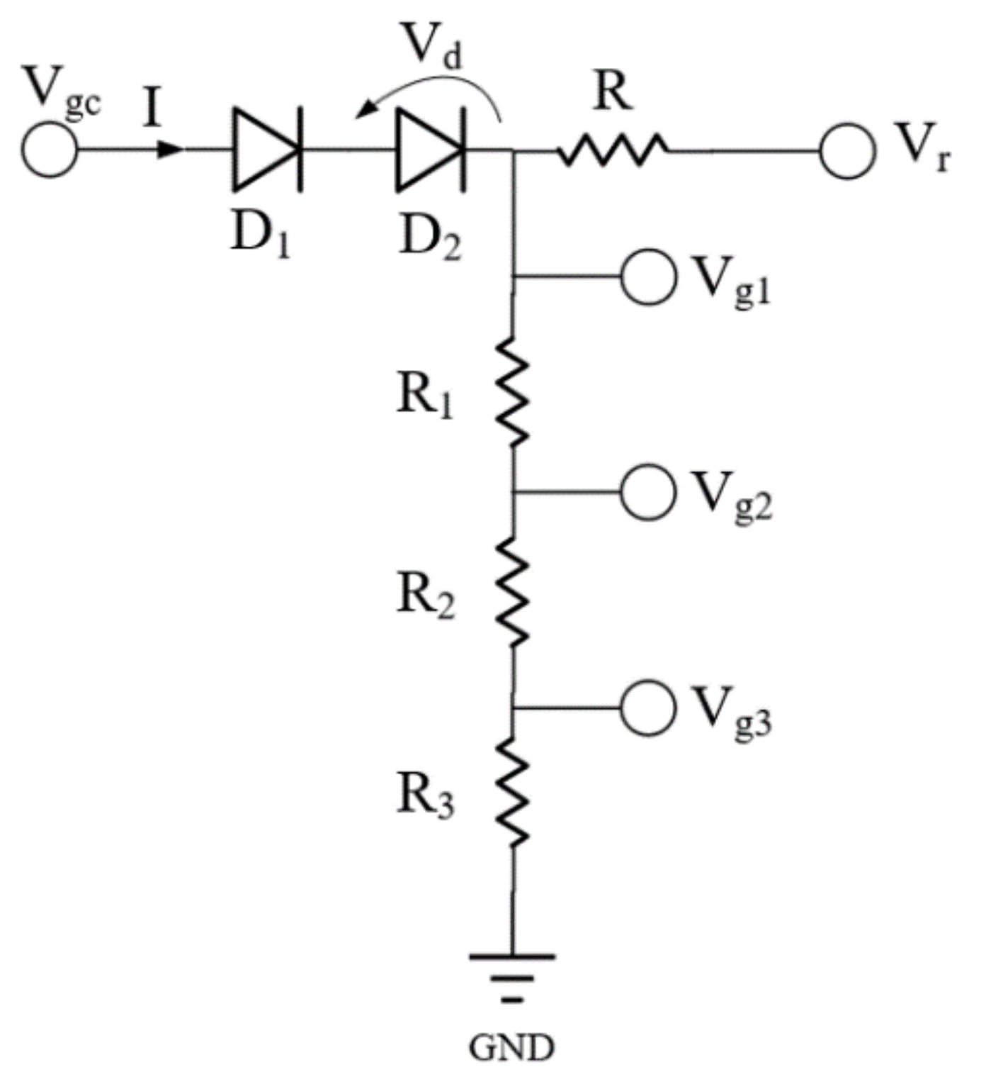
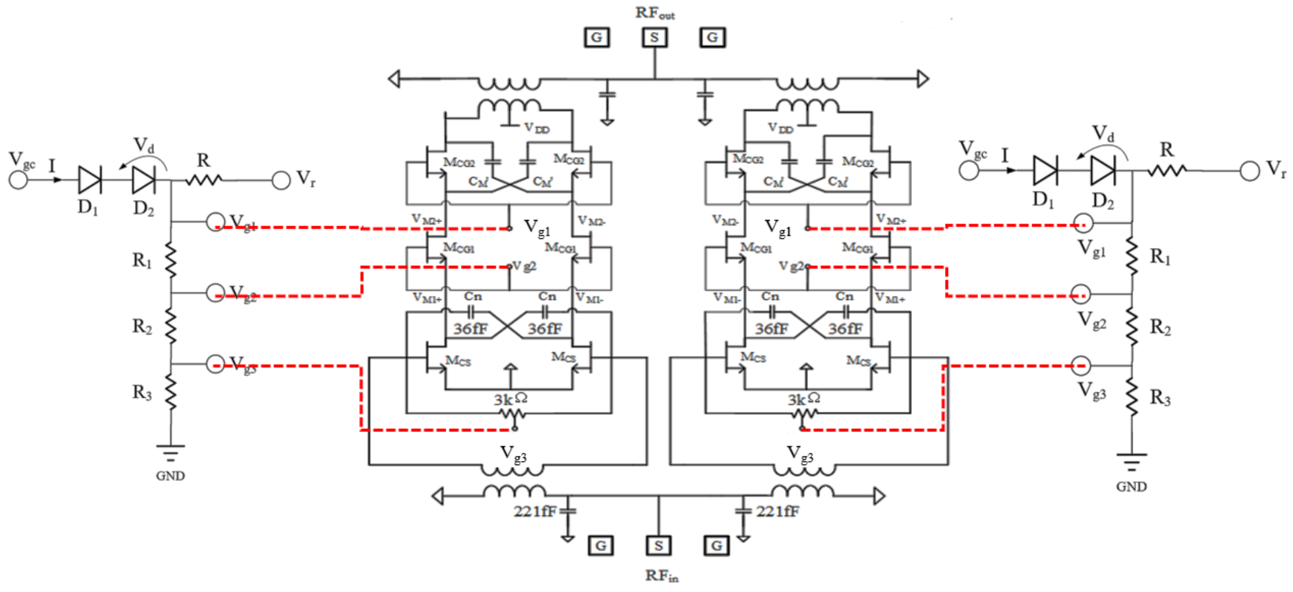
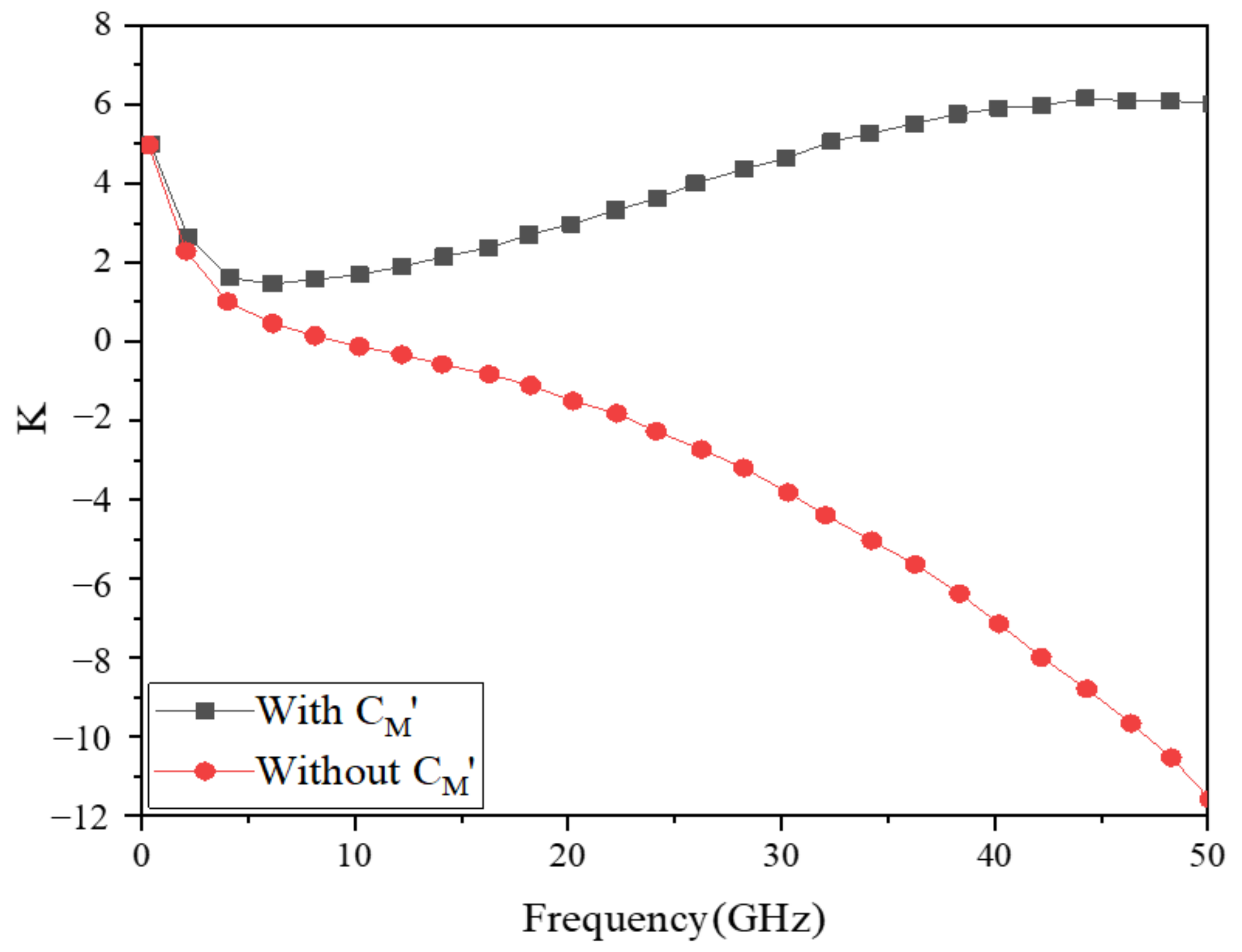
3. Principle and Design of Temperature Compensation Circuit

As described in Section 1, increasing the gate voltage can compensate for the change in amplifier gain. This temperature compensation circuit consists of two diodes and four resistors, as shown in Figure 2. The values of gate voltages Vg1, Vg2, and Vg3 are determined by the Vr and Vgc. In Figure 2, D1 and D2 are diodes, R, R1, R2, and R3 are resistors, and Vd and I are the current and voltage through the diodes, respectively. The compensation circuit shown in Figure 2 utilizes the mechanism whereby the threshold voltage of the diode decreases with increasing temperature.
To facilitate the presentation of the operating principle of the temperature compensation circuit, it is assumed that Vgc = 0. The following equation can be derived from Figure 2 [31].
- V r = R I + 2 V d ,
I = I s exp ( q V d n k T ) 1 ,
where T is the temperature, and n is the ideal coefficient of the diode. Is can be expressed as
I s = S A * T 2 exp ( q ϕ B k T ) ,
where A* is the temperature-independent Richardson–Dushman constant, φB is the material-dependent Schottky barrier voltage, and S is the junction size of the diode. From (2), (3), and (4), it follows that Vg1 is a function of T:
V g 1 = 2 k T q ln ( S R A * ) + 2 k T q ln ( T ) ϕ B n ,
where Vg1 = −2Vd (as shown in Figure 2).
Assume that RIs ≪ −(Vr + 2Vd) ≪ (1/RIs). Then, from (4), the following equation can be derived.
V g 1 T = 2 n k q ln ( S R A * ) + 2 ln ( T ) + 2 ,
If T is greater than −270 °C, we have ∂Vg1/∂T > 0. Vg1 increases with increasing temperature for T greater than −270 °C. The following equation can calculate the variation of Vg1Vg1) between two temperatures, TH and TL.
Δ V g 1 = T L T H V g 1 T d T = T L T H 2 n k q ln ( S R A * ) + 2 ln ( T ) + 2 d T = 2 n k q ( T H T L ) ln ( S R A * ) + 4 n k q ( T H l n ( T H ) T L l n ( T L ) )
Therefore, the expressions for Vg2 and Vg3 can be obtained according to Figure 2 and Equation (5).
V g 2 = V g 1 R 2 + R 3 R 1 + R 2 + R 3 ,
V g 3 = V g 1 R 3 R 1 + R 2 + R 3 ,
According to (8) and (9), Vg2 and Vg3 are proportional to Vg1, increasing with temperature. Therefore, Vg2 and Vg3 also increase with temperature in order to realize gain compensation. The following explains the compensation circuit’s principle to compensate for the PA’s small-signal gain.
When the temperature increases, gate voltage Vg1, gate voltage Vg2, and gate voltage Vg3 in the temperature compensation circuit all increase as the temperature increases. The increase in gate voltage Vg1, gate voltage Vg2, and gate voltage Vg3 is equivalent to the rise in the magnitude of VGS of Equation (1). When Vg1, Vg2, and Vg3 increase with temperature, the transconductance of each layer of the stacked PA can be expressed as
g 1 = I D ( s a t ) V G S = μ n ( T 0 ) ( T T 0 ) 3 / 2 W C o x L ( V g 1 + Δ V g 1 V T ) ,
g 2 = I D ( s a t ) V G S = μ n ( T 0 ) ( T T 0 ) 3 / 2 W C o x L ( V g 2 + Δ V g 2 V T ) ,
g 3 = I D ( s a t ) V G S = μ n ( T 0 ) ( T T 0 ) 3 / 2 W C o x L ( V g 3 + Δ V g 3 V T ) ,
According to Equations (10)–(12), the transconductance (i.e., gain) of each layer increases with ΔVg1, ΔVg2, and ΔVg3, i.e., with the increase in temperature. Thus, the compensation for the degradation of the gain of each layer with the increase in temperature is achieved.
It should be noted that the on-chip temperature compensation circuit described in this section does not have any additional requirements or constraints on the design of the PA. In addition, the compensation circuit was designed for a single-stage PA. Specifically, for a multi-stage PA, the parameters of each transistor stage are different. Then, it is necessary to determine the value of ΔVg, similar to the one shown in Figure 1, based on the parameters of each transistor stage. From Equation (7), it can be seen that the parameters affecting ΔVg1 are mainly the junction size (S) and resistance (R) of the diode. Therefore, for a multi-stage PA, the design of the corresponding temperature compensation circuit can be completed by simply adjusting the values of S and R so that the ΔVg1 (as shown in Equation (7)) of each stage meets the requirements similar to the ΔVg1 in Figure 1.

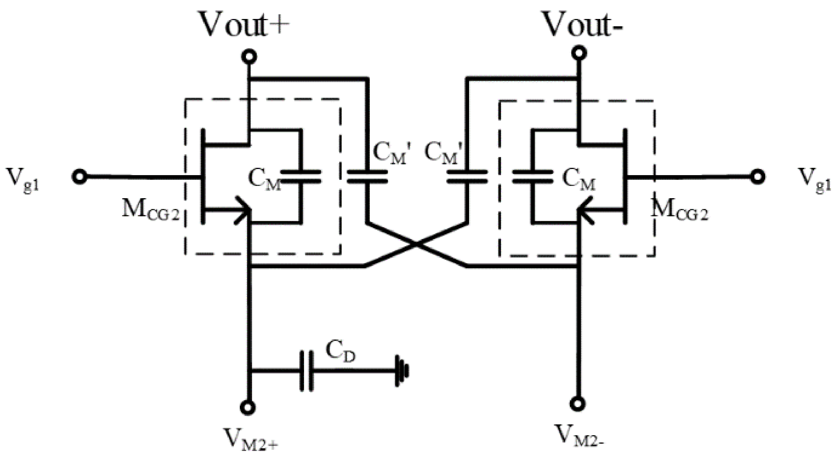
4. Differential Stacked Millimeter-Wave Broadband PA

To verify the effectiveness of the proposed on-chip temperature compensation circuit, a differential stacked millimeter-wave wideband PA was implemented in this study. Figure 3 shows the schematic of a differential stacked millimeter-wave wideband PA, which is used to compensate for the degradation of small-signal gain. As shown in Figure 1, the required ΔVg1 is 0.1 V. Two diodes are connected in series to achieve ΔVg1 = 0.1 V.
Differential common-source structures [32,33] and stacked structures [34,35] are two circuit topologies commonly used in PA design. The differential common-source structure can suppress even harmonics. In contrast, the stacked structure can achieve a large output voltage swing (i.e., the transistors are connected in series to achieve a superposition of bias voltages and increase the output voltage swing of the PA) while ensuring that the transistors do not break down, thus increasing the output power of the PA. We designed and implemented a differential triple-stacked millimeter-wave broadband PA with on-chip temperature compensation based on the differential common-source structure and stacked structure.
The PA uses a two-way differential stacking structure to increase the output power and improve the stability of the PA by introducing a negative feedback network. To increase the bandwidth and reduce losses, on-chip transformers were used for the matching networks at the input/output of the PAs designed in this study. A thick metal layer was used in the design process for the on-chip transformer and interconnecting lines. As shown in Figure 3, the gate width/gate length of transistors MCG2, MCG1, and MCS were 4 × 60 μm/60 nm, 4 × 60 μm/60 nm, and 3 × 60 μm/60 nm, respectively. Meanwhile, to improve power gain, isolation, and gain flatness, the neutralizing capacitor (Cn), shunt capacitor (Cin), and shunt resistor (Rg), respectively, were introduced in this study.
Although introducing a neutralization capacitor (Cn) can improve the stability of a PA to some extent, the PA will still be unstable when the parasitic capacitance (CM) between the source and drain of transistor MCG2 is relatively large. This is also one of the main reasons for the instability of the stacked structure amplifier. Therefore, as shown in Figure 4, this study introduced another capacitor (CM’) in the negative feedback network of the top layer in order to improve stability. The capacitor (CD) is the raw capacitance of the drain of transistor, MCG1. The regulation of CM’ is used to achieve a balance between the three capacitors CM’, CM, and CD in order to achieve the stability of the PA.
The stability of the PA is shown in Figure 5. According to Figure 5, this PA’s stability factor (K) in the range of 0–5 GHz was greater than 1 without introducing CM’, and the PA was in a stable state. The StabFact in the other frequency ranges was less than 1, and the PA was in an unstable condition. When CM’ was introduced into the PA, the stability factor of the PA in the whole frequency range was always greater than 1. As a result, the PA remained stable over the entire operating frequency range. This indicates that the introduction of capacitance (CM’) in the negative feedback network of the top layer of this stacked PA can effectively improve the stability of the PA.
Figure 6 shows the core layout and overall layout of a differential stacked millimeter-wave wideband PA. The layout of the PA has a significant impact on the performance of the PA. Therefore, to simplify the RF signal path to reduce power consumption, we kept the layout of transistors MCG1 and MCG2 in the stacked structure, shown Figure 3, perpendicular to the direction of transistor MCS when laying out the PA. The overall area of the PA chip was 0.378 mm2.

5. Results and Discussion

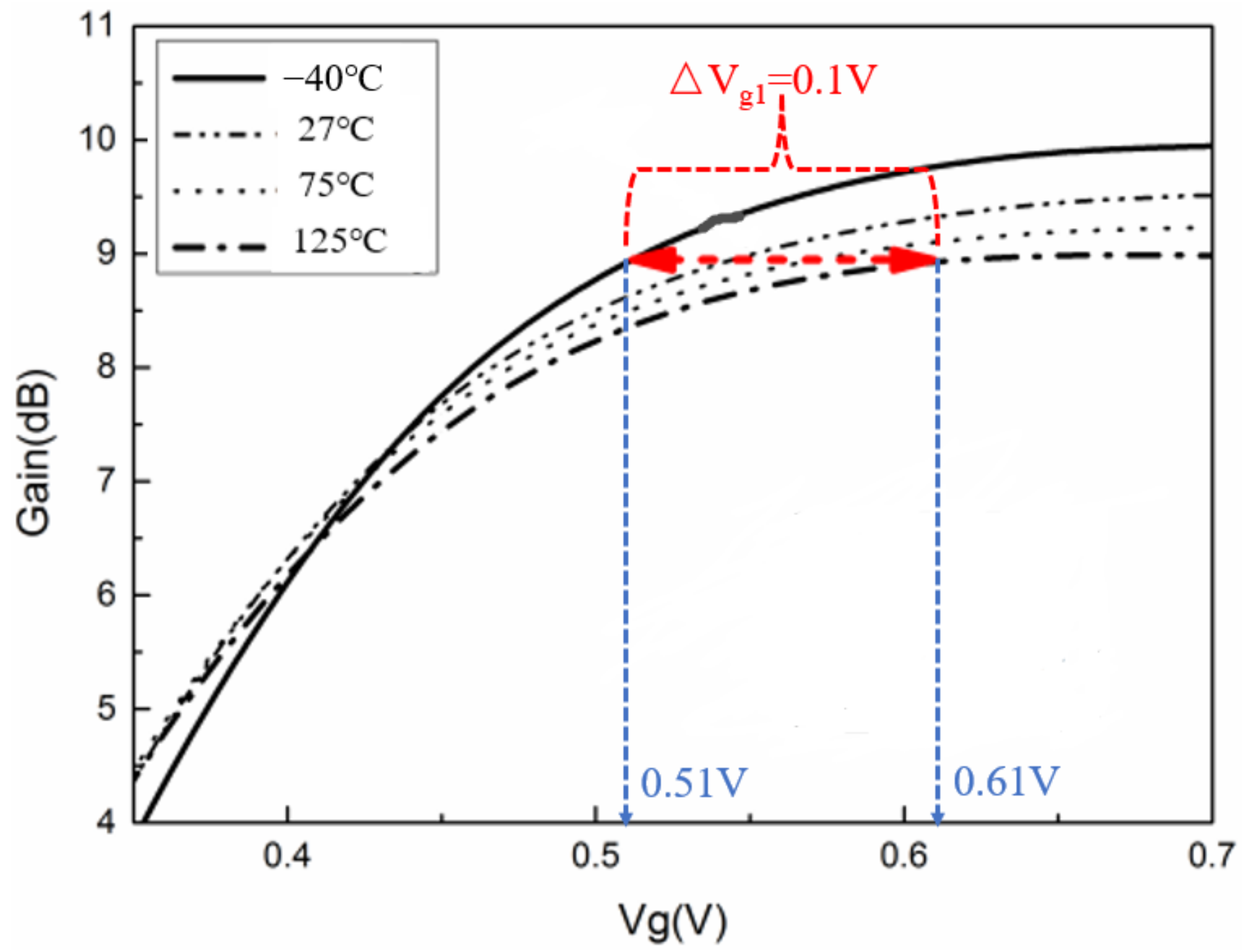
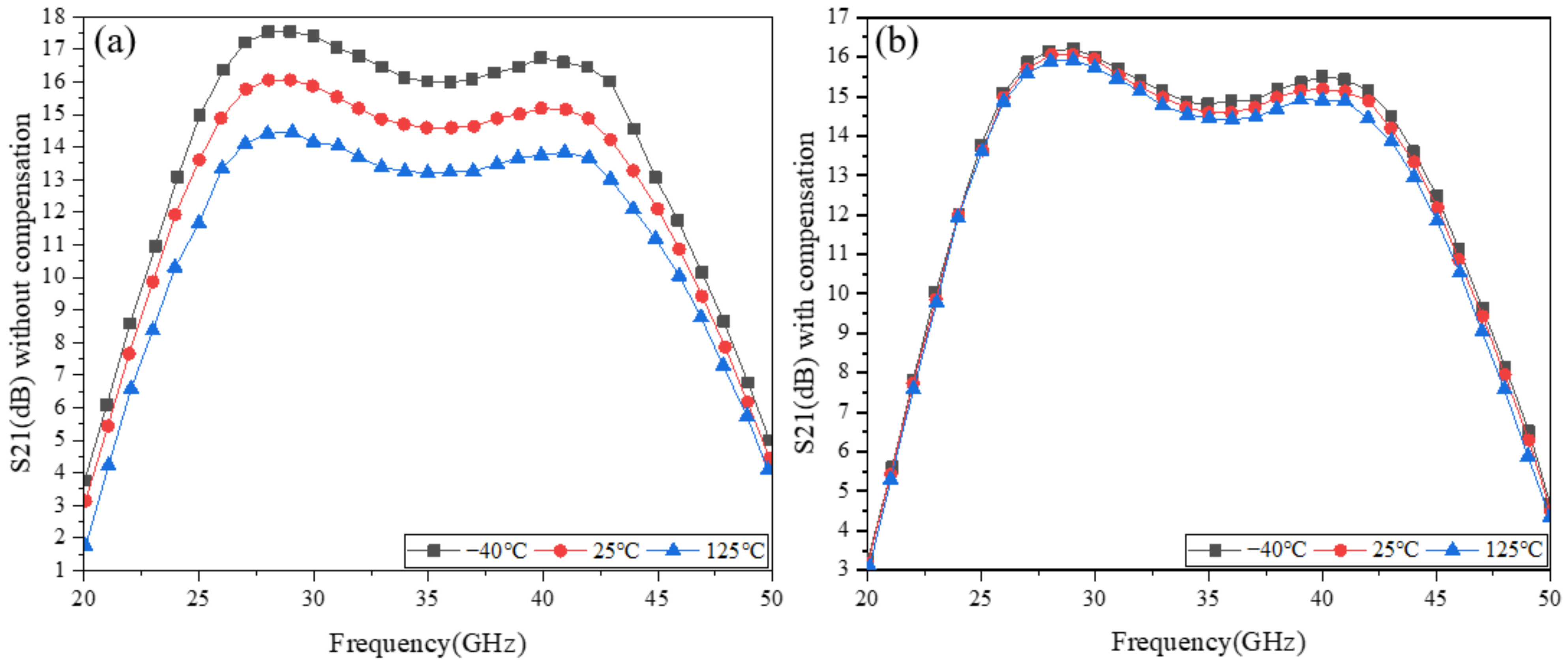
5.1. Small-Signal Gain at Different Temperatures

Figure 7 gives the small-signal gain versus temperature variation for the differential stacked millimeter-wave broadband power amplifier. Figure 7a,b show the results without and with temperature compensation circuits, respectively.
As seen in Figure 7, without the compensation, the small-signal gain varied by 2.4 dB in the frequency range of 25–40 GHz, while with the compensation, the small-signal gain varied by 0.1 dB in the frequency range of 25–40 GHz. The specific reasons are discussed below.
The small-signal gain is the transconductance [29], and the expression for the transconductance is
g m = 2 μ n C o x W L I d s ,
and the main factors affecting the transconductance are μn and Ids, where the expression for the drain current in the saturation region is [36]
I d s = μ n C o x ( W L ) ( V g s V t h ) 2 ,
where Vgs is the gate voltage, and Vth is the threshold voltage.
When Vgs increases, Ids also increases with the rise of Vgs. It is also known from Equation (13) that the small-signal gain increases as Ids increases. When the temperature rises, μn decreases with the increase in temperature, resulting in a reduction in small-signal gain. With the compensation, Ids increases as the temperature rises to effectively compensate for the degradation of the small-signal gain due to μn. In other words, the gate voltage Vg1, gate voltage Vg2, and gate voltage Vg3 increase with the temperature, which increases the Ids, and thus, compensates for the small-signal gain. This indicates that the on-chip temperature compensation circuit has a good compensation effect on the small-signal gain.

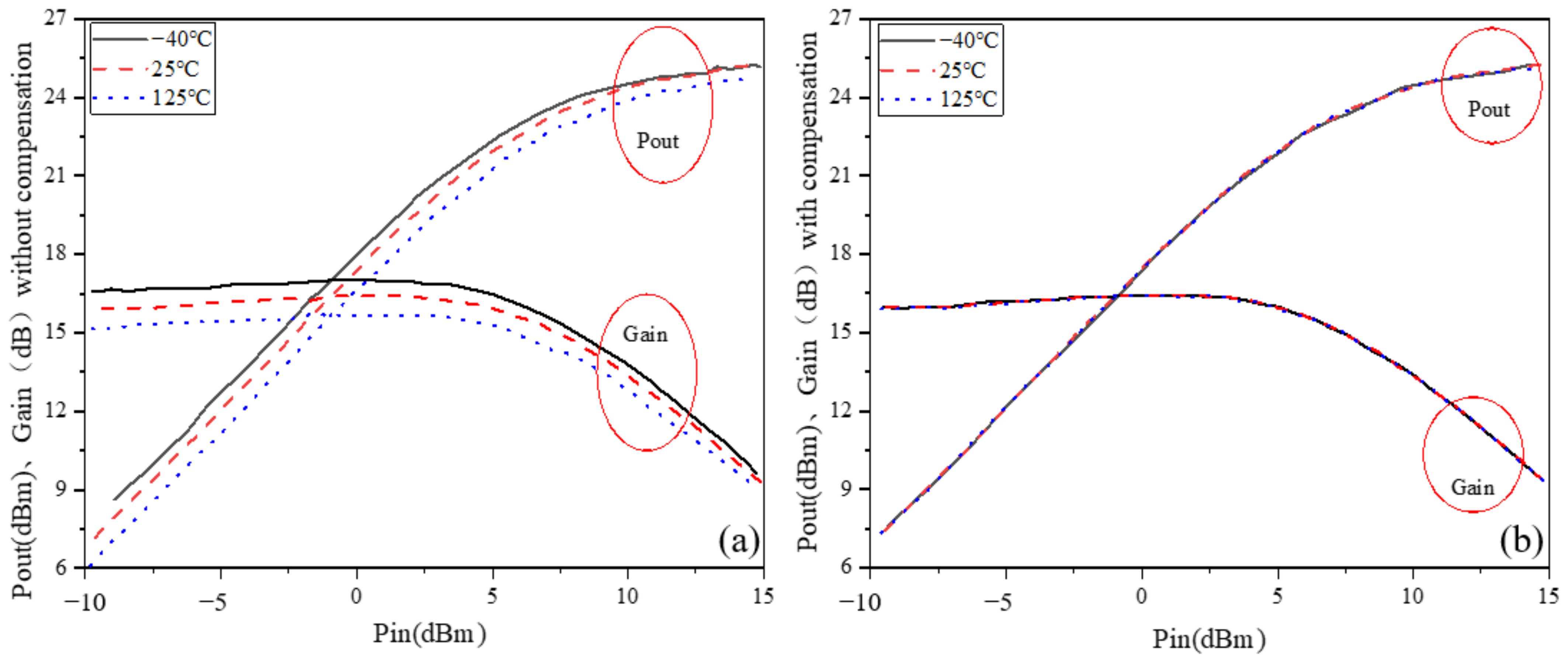
5.2. Output Power and PAE at Different Temperatures

The output power (Pout) and large-signal gain at the center frequency of the PA versus temperature are shown in Figure 8. As shown in Figure 8a, the Pout and large-signal gain with an on-chip temperature compensation circuit varied very little. In contrast, the PA’s output power and large-signal gain without a temperature compensation circuit were more significantly affected by temperature variations.
The power-added efficiency (PAE) at the center frequency of the PA versus temperature is shown in Figure 9. It is worth noting that the effect of temperature on the PA’s power-added efficiency was relatively large, regardless of whether it was with compensation. This indicates that the compensation circuit has a better compensation effect on the Pout and large-signal gain, while the compensation effect on the PAE is insignificant. The specific reasons are discussed below.
Literature studies have shown [37] that the on-state resistance between source and drain increases with temperature, which leads to a drop in the Pout. The expression for on-resistance is [37]
R o n = R 0 + k T α / V g s V t h β ,
where the constant k is a process parameter, R0 is a constant independent of voltage and temperature, α ≈ 1.5, β ≈ 0.2, Vgs is the gate voltage, and Vth is the threshold voltage.
According to Equation (15), on-resistance increases with increasing temperature. Therefore, when the PA does not have a temperature compensation circuit, the Pout decreases with increasing temperature. On the other hand, when the PA is with compensation, the gate Vgs in Equation (15) increases with the temperature, causing the on-resistance to decrease with the gate voltage increase, thus achieving the compensation for the Pout. As a result, the compensation for the large-signal gain is also achieved. As for the PAE, the compensation circuit compensates for the Pout while increasing the DC power consumption of the PA [24]. Therefore, according to the definition of PAE, the PAE decreases with the increase in DC power consumption. Thus, with or without compensation, the effect of temperature change on PAE of PA is relatively significant [24].
Table 1 compares the amplifier’s performance with on-chip temperature compensation circuits. Compared with the compensation circuit structures and methods in the literature [23,24,38,39,40], the temperature compensation circuit proposed in this paper has a simple structure, a smaller overall chip area, and a better compensation effect for small-signal gain and output power. Still, the compensation effect for PAE was poor. In addition, these post-layout simulation results can be regarded as a supplement to the measured results in Refs. [23,38,39,40]. This idea is consistent with Ref. [24], and these results are effective in the relative amount of change in small-signal gain, output power, and PAE before and after compensation.
Furthermore, in terms of the magnitude of small-signal gain variation with temperature, the compensation circuit can effectively compensate for the small-signal gain. This shows that the proposed compensation circuit for differential stacked millimeter-wave wideband PAs effectively compensates for the degradation of the small-signal gain of PAs due to temperature variations over a wide range.

6. Conclusions

This paper proposes a compensation circuit consisting of two diodes and four resistors for a PA with a stacked structure. To verify the effectiveness of the compensation circuit, we designed and implemented a differential triple-layer stacked structure millimeter-wave wideband PA.
With the temperature-compensation circuit, the small-signal gain variation improved from 2.4 to 0.1 dB in the temperature range between −40 °C and 125 °C. It was demonstrated that the proposed on-chip temperature compensation circuit effectively corrects the small-signal gain, large-signal gain, and Pout variations of a millimeter-wave PA with a multi-layer stacked structure over a wide temperature range. In addition, the proposed on-chip temperature compensation circuit also applies to multi-stage cascaded microwave/mm-wave power amplifiers.

Author Contributions

Conceptualization, S.Z., S.W. and J.W.; methodology, S.Z., S.W. and J.W.; software, S.Z. and S.W.; validation, S.Z., S.W. and J.W.; formal analysis, J.W.; investigation, S.Z. and S.W.; resources, J.W.; data curation, S.Z. and S.W.; writing—original draft preparation, S.Z.; writing—review and editing, S.W. and J.W.; visualization, S.Z. and S.W.; supervision, J.W.; project administration, J.W.; funding acquisition, J.W. All authors have read and agreed to the published version of the manuscript.

Funding

This research was supported by the State Key Laboratory of Complex Electromagnetic Environment Effects on Electronics and Information System (No. CEMEE2022G0201, CEMEE-002-20220224).

Conflicts of Interest

The authors declare no conflict of interest.

References

  1. Wang, X.D.; Lv, X.; Guo, D.L.; Li, M.X.; Cheng, G.; Liu, J.S.; Yu, W.H. Terahertz power amplifier integrated with on-chip antenna using GaN TMIC technology. J. Infrared Millim. Waves 2019, 38, 683–689. [Google Scholar]
  2. Zhu, H.B.; Wei, H.; Tian, L.; Hong-Jun, T.; Ji-Xin, C.; Fan-Fan, H. Design and fabrication of Ka-band broadband combined power amplifier based on flexible substrate integrated waveguide technology. J. Infrared Millim. Waves 2010, 29, 180–184. [Google Scholar] [CrossRef]
  3. Huang, Z.Y.; Jun, X.U.; Ran, D.; Qi, Y.F. Design of a W-band power amplifier/combiner based on spatial power-combining technique. J. Infrared Millim. Waves 2018, 37, 454–458. [Google Scholar]
  4. Cao, Y.X.; Su, Y.B.; Wu, D.Y.; Jin, Z.; Wang, X.T.; Liu, X.Y. A 75 GHz 13.92 dBm InP DHBT cascode power amplifier. J. Infrared Millim. Waves 2012, 31, 294–297. [Google Scholar] [CrossRef]
  5. Yang, F.; Zhao, H.F.; Liu, J.T.; Liu, R.Z.; Liu, Y.P.; Hu, F.J.; Sun, S.; Feng, Y.U.; Zhou, Y. Solid-state power amplifiers for space: Going to extremely high frequency. J. Infrared Millim. Waves 2021, 40, 25–32. [Google Scholar]
  6. Karra, A.; Kondi, B.; Jayaraman, R. Implementation of wireless communication to transfer temperature and humidity monitoring data using Arduino Uno. In Proceedings of the 2020 International Conference on Communication and Signal Processing (ICCSP), Chennai, India, 28–30 July 2020; pp. 1101–1105. [Google Scholar]
  7. Chiang, C.Y.; Hsu, H.T.; Chang, E.Y. Monolithic wideband linear power amplifier with 45% power bandwidth using pseudomorphic high-electron-mobility transistors for long-term evolution application. Jpn. J. Appl. Phys. 2014, 53, 110311. [Google Scholar] [CrossRef]
  8. Giammello, V.; Ragonese, E.; Palmisano, G. A 15-dBm SiGe BiCMOS PA for 77-GHz Automotive Radar. IEEE Trans. Microw. Theory Tech. 2011, 59, 2910–2918. [Google Scholar] [CrossRef]
  9. Chen, B.; Lou, L.; Tang, K.; Wang, Y.; Gao, J.; Zheng, Y. A 13.5–19 GHz 20.6-dB Gain CMOS Power Amplifier for FMCW Radar Application. IEEE Microw. Wirel. Compon. Lett. 2017, 27, 377–379. [Google Scholar] [CrossRef]
  10. Ge, Q.; Liu, W.; Xu, B.; Qian, F.; Yao, C. A 77–100 GHz power amplifier using 0.1-μm GaAs PHEMT technology. J. Semicond. 2017, 38, 120–123. [Google Scholar] [CrossRef]
  11. Rautschke, F.; Maassen, D.; Ohnimus, F.; Schenk, L.; Dalisda, U.; Boeck, G. A hybrid 50-W GaN-HEMT Ku-band power amplifier. In Proceedings of the 2016 46th European Microwave Conference (EuMC), London, UK, 3–7 October 2016; pp. 1079–1082. [Google Scholar]
  12. Maassen, D.; Rautschke, F.; Boeck, G. Design and comparison of various coupled line Tx-filters for a Ku-band block upconverter. In Proceedings of the 2016 German Microwave Conference (GeMiC), Bochum, Germany, 14–16 March 2016; pp. 225–228. [Google Scholar]
  13. Wang, K.; Cheng, Z.; Fan, K.; Chen, S.; Liu, G.; Wang, H. High-efficiency power amplifier for Beidou satellite navigation system. In Proceedings of the 2015 IEEE 16th International Conference on Communication Technology (ICCT), Hangzhou, China, 18–20 October 2015; pp. 655–657. [Google Scholar]
  14. China Talking about the “Shelf Life” of Missiles. Military. Available online: http://www.81.cn/jfjbmap/content/2018-03/09/content_201251.htm (accessed on 9 March 2018).
  15. Wu, S.B.; Gao, J.F.; Wang, W.B.; Zhang, J.Y. W-Band MMIC PA With Ultrahigh Power Density in 100-nm AlGaN/GaN Technology. IEEE Trans. Electron Devices 2016, 63, 3882–3886. [Google Scholar]
  16. Qi, T.; He, S.; Shi, W. Third-octave power amplifier using ring-based matching network with high efficiency. Electron. Lett. 2016, 52, 883–885. [Google Scholar] [CrossRef]
  17. Zhou, S.; Fu, H.; Ma, J.; Zhang, Q. A neural network modeling approach to power amplifiers taking into account temperature effects. In Proceedings of the 2018 IEEE/MTT-S International Microwave Symposium, Philadelphia, PA, USA, 10–15 June 2018; pp. 1028–1031. [Google Scholar]
  18. Ma, X.; Duan, B.; Yang, Y. A 500–600 MHz GaN power amplifier with RC-LC stability network. J. Semicond. 2017, 38, 085003. [Google Scholar] [CrossRef]
  19. Yu, C.; Yuan, J.S. Electrical and Temperature Stress Effects on Class-AB Power Amplifier Performances. IEEE Trans. Electron Devices 2007, 54, 1346–1350. [Google Scholar]
  20. Cheng, J.H.; Wu, M.H.; Huang, H.T.; Wu, Y.M.; Tsai, J.H.; Huang, T.W. A K-band phase-locked loop in 0.18 μm CMOS technology for vital sign detection radar. In Proceedings of the 2014 IEEE MTT-S International Microwave Workshop Series on RF and Wireless Technologies for Biomedical and Healthcare Applications (IMWS-Bio2014), London, UK, 1–3 December 2014. [Google Scholar]
  21. Gs, J.; Banerj, E.G.; Raja, I. On-chip non-intrusive temperature detection and compensation of a fully integrated CMOS RF power amplifier. In Proceedings of the 2017 30th International Conference on VLSI Design and 2017 16th International Conference on Embedded Systems (VLSID), Hyderabad, India, 21–26 January 2017. [Google Scholar]
  22. Wenger, Y.; Meinerzhagen, B.; Ghazinour, A. Current-mode temperature compensation for a differential logarithmic amplifier in 180 nm BiCMOS. In Proceedings of the 2018 25th IEEE International Conference on Electronics, Circuits and Systems (ICECS), Bordeaux, France, 9–12 December 2018; pp. 509–512. [Google Scholar]
  23. Qi, Q.; Chen, Z. A K-Band CMOS Amplifier with Temperature Compensation for Gain Variation Reduction. IEEE Microw. Wirel. Compon. Lett. 2018, 28, 150–152. [Google Scholar] [CrossRef]
  24. Pour, F.L.; Ha, D.S. A Temperature compensated 5 GHz GaN on SiC power amplifier. In Proceedings of the 2020 IEEE 63rd International Midwest Symposium on Circuits and Systems (MWSCAS), Springfield, MA, USA, 9–12 August 2020; pp. 549–553. [Google Scholar]
  25. Li, S.; Fritsche, D.; Carta, C.; Ellinger, F. Design and characterization of a 12–40 GHz power amplifier in SiGe technology. In Proceedings of the 2018 IEEE Topical Conference on RF/Microwave Power Amplifiers for Radio and Wireless Applications (PAWR), Anaheim, CA, USA, 23–25 January 2018. [Google Scholar]
  26. Pascht, A.; Grozing, M.; Wiegner, D.; Berroth, M. Small-Signal and Temperature Noise Model for MOSFETs. IEEE Trans. Microw. Theory Tech. 2002, 50, 1927–1934. [Google Scholar] [CrossRef]
  27. Zhao, D.; Reynaert, P. A 40-nm CMOS E-Band 4-Way Power Amplifier with Neutralized Bootstrapped Cascode Amplifier and Optimum Passive Circuits. IEEE Trans. Microw. Theory Tech. 2015, 63, 4083–4089. [Google Scholar] [CrossRef]
  28. Razavi, B. Design of Analog CMOS Integrated Circuits; McGraw Hill Higher Education: New York, NY, USA, 2003; pp. 17–21. [Google Scholar]
  29. Neamen, D.A. Semiconductor Physics and Devices: Basic Principles; McGraw Hill Higher Education: New York, NY, USA, 2012; pp. 395–419. [Google Scholar]
  30. Lee, T.H. The Design of CMOS Radio-Frequency Integrated Circuits; Cambridge University Press: Cambridge, UK, 2012; pp. 172–189. [Google Scholar]
  31. Yamauchi, K.; Iyama, Y.; Yamaguchi, M.; Ikeda, Y.; Urasaki, S.; Takagi, T. X-band MMIC power amplifier with an on-chip temperature-compensation circuit. IEEE Trans. Microw. Theory Tech. 2001, 49, 2501–2506. [Google Scholar] [CrossRef]
  32. Wu, K.; Muralidharan, S.; Hella, M. A 104GHz–117GHz power amplifier with 10.4% PAE in thin digital 65 nm low power CMOS technology. In Proceedings of the 2016 IEEE MTT-S International Microwave Symposium (IMS), San Francisco, CA, USA, 1–3 May 2016. [Google Scholar]
  33. Lin, Y.S.; Gao, J.W.; Wang, C.C.; Lin, Y.W.; Chen, C.C. A wideband power amplifier with 13.2 dBm Psat and 19.5% PAE for 60~94 GHz wireless communication systems in 90 nm CMOS. In Proceedings of the 2016 IEEE Radio and Wireless Symposium (RWS), Austin, TX, USA, 24–27 January 2016; pp. 95–98. [Google Scholar]
  34. Thome, F.; Leuther, A.; Schlechtweg, M.; Ambacher, O. Broadband high-power W-band amplifier MMICs based on stacked-HEMT unit cells. IEEE Trans. Microw. Theory Tech. 2018, 66, 1312–1318. [Google Scholar] [CrossRef]
  35. Chen, T.; Tian, T.; Wu, J.H.; Gao, H. Design of a 5.8 GHz Stacked Power Amplifier. J. Microw. 2014, 30, 77–79. [Google Scholar]
  36. Zhou, S. Experimentally investigating the degradations of small-signal gain for a GaN class-AB dual-band power amplifier under high temperature and humidity conditions. AIP Adv. 2020, 10, 125219. [Google Scholar] [CrossRef]
  37. He, Z.; Zhou, S.; Nie, M. Experimentally investigating the performance degradations of the CMOS PA at different temperatures. AIP Adv. 2021, 11, 115205. [Google Scholar] [CrossRef]
  38. Kaamouchi, M.E.; Moussa, M.S.; Raskin, J.P.; Vanhoenacker-Janvier, D. Zero-temperature-coefficient biasing point of 2.4-GHz LNA in PD SOI CMOS technology. In Proceedings of the 2007 European Microwave Conference, Munich, Germany, 9–12 October 2007; pp. 1101–1104. [Google Scholar]
  39. Chen, W.L.; Chang, S.F.; Chen, K.M.; Huang, G.W.; Chang, J.C. Temperature Effect on Ku-Band Current-Reused Common-Gate LNA in 0.13 μm CMOS Technology. IEEE Trans. Microw. Theory Tech. 2009, 57, 2131–2138. [Google Scholar] [CrossRef]
  40. Motoyoshi, M.; Takano, K.; Yoshida, T.; Katayama, K.; Amakawa, S.; Minoru, F. 79 GHz CMOS power amplifier using temperature compensation bias. In Proceedings of the 2014 9th European Microwave Integrated Circuit Conference, Rome, Italy, 6–7 October 2014; pp. 49–52. [Google Scholar]
Figure 1. Temperature characteristics of gain of single-stage PA.
Micromachines 13 01101 g001
Figure 2. Schematic diagram of the compensation circuit.
Micromachines 13 01101 g002
Figure 3. Schematic diagram of differential stacked PA, based on temperature compensation circuit.
Micromachines 13 01101 g003
Figure 4. Schematic diagram of the negative feedback network.
Micromachines 13 01101 g004
Figure 5. Stability factor of PA.
Micromachines 13 01101 g005
Figure 6. PA’s overall layout and core layout: (a) core layout; (b) overall layout.
Micromachines 13 01101 g006
Figure 7. Small-signal gain versus temperature variation: (a) without temperature compensation; (b) with temperature compensation.
Micromachines 13 01101 g007
Figure 8. Output power versus temperature variation: (a) without temperature compensation; (b) with temperature compensation.
Micromachines 13 01101 g008
Figure 9. PAE versus temperature variation: (a) without temperature compensation; (b) with temperature compensation.
Micromachines 13 01101 g009
Table 1. Performance comparison with previous works.
ReferenceRef. [23]Ref. [38]Ref. [39]Ref. [40]Ref. [24] This Work
CircuitPALNALNAPAPAPA
Technology90 nm130 nm SOI130 nm40 nmGaN HEMT55 nm
Topology2-stage1-stage1-stage3-stage1-stage1-stage
Frequency (GHz)26.52.415.2794.5–5.525–40
Small-signal gain variation (dB)1.2
(−45~125 °C)
0.9
(25~200 °C)
3.1
(−20~120 °C)
0.6
(10~100 °C)
0.4
(−40~225 °C)
0.1
(−40~125 °C)
Pout variation (dBm)
(center frequency)
N/AN/AN/AN/A24.0
(−40~225 °C)
0.6
(−40~125 °C)
PAE variation
(center frequency)
N/AN/AN/AN/A12%
(−40~225 °C)
7.3%
(−40~125 °C)
Area (mm2)0.5 0.6 0.6 0.11 6.60.378
Note: DC pads are not included. Post-layout simulation results.
Publisher’s Note: MDPI stays neutral with regard to jurisdictional claims in published maps and institutional affiliations.

