
Investigation of the Specification Degradation Mechanism of CMOS Power Amplifier under Thermal Shock Test


Abstract
:1. Introduction
2. Designed PA and the Experimental Setup
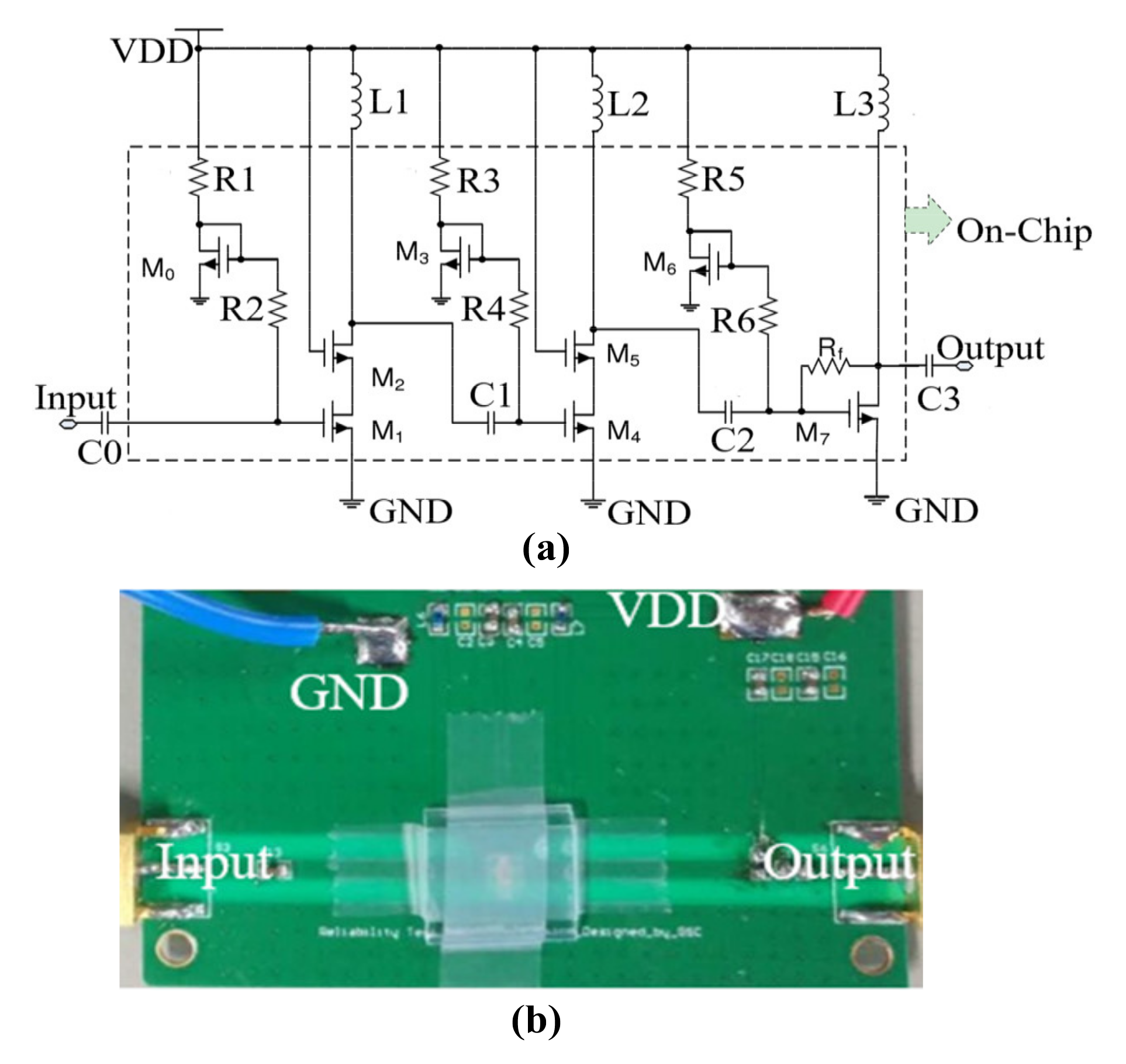
2.1. The Designed PA
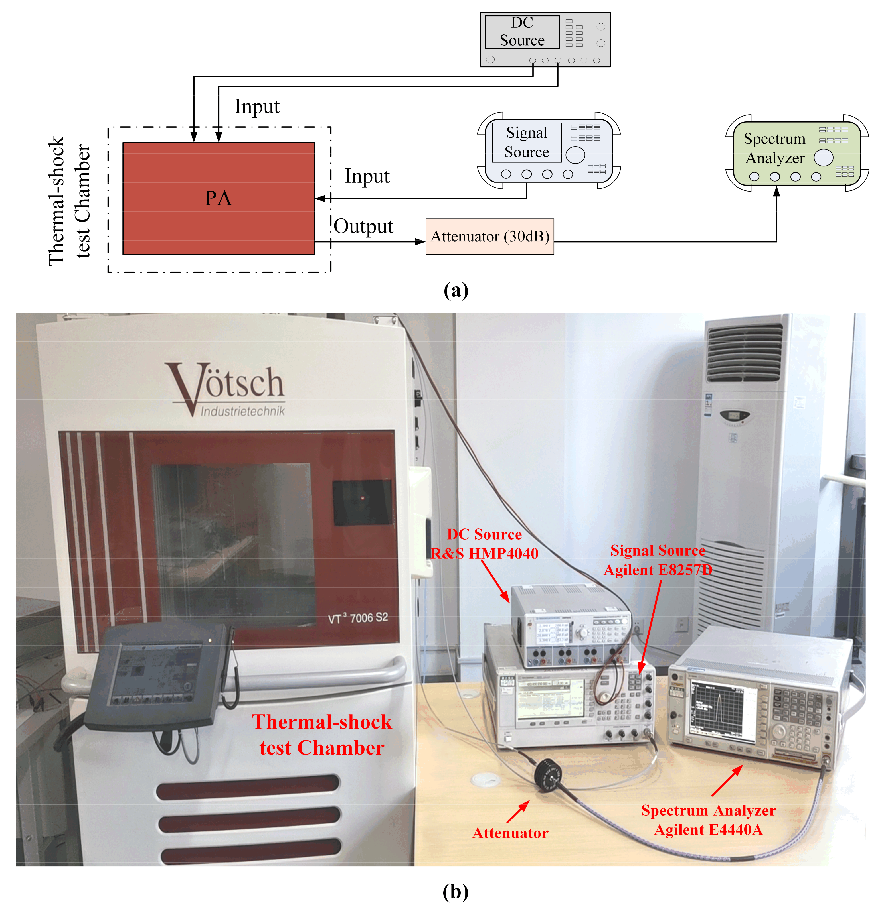
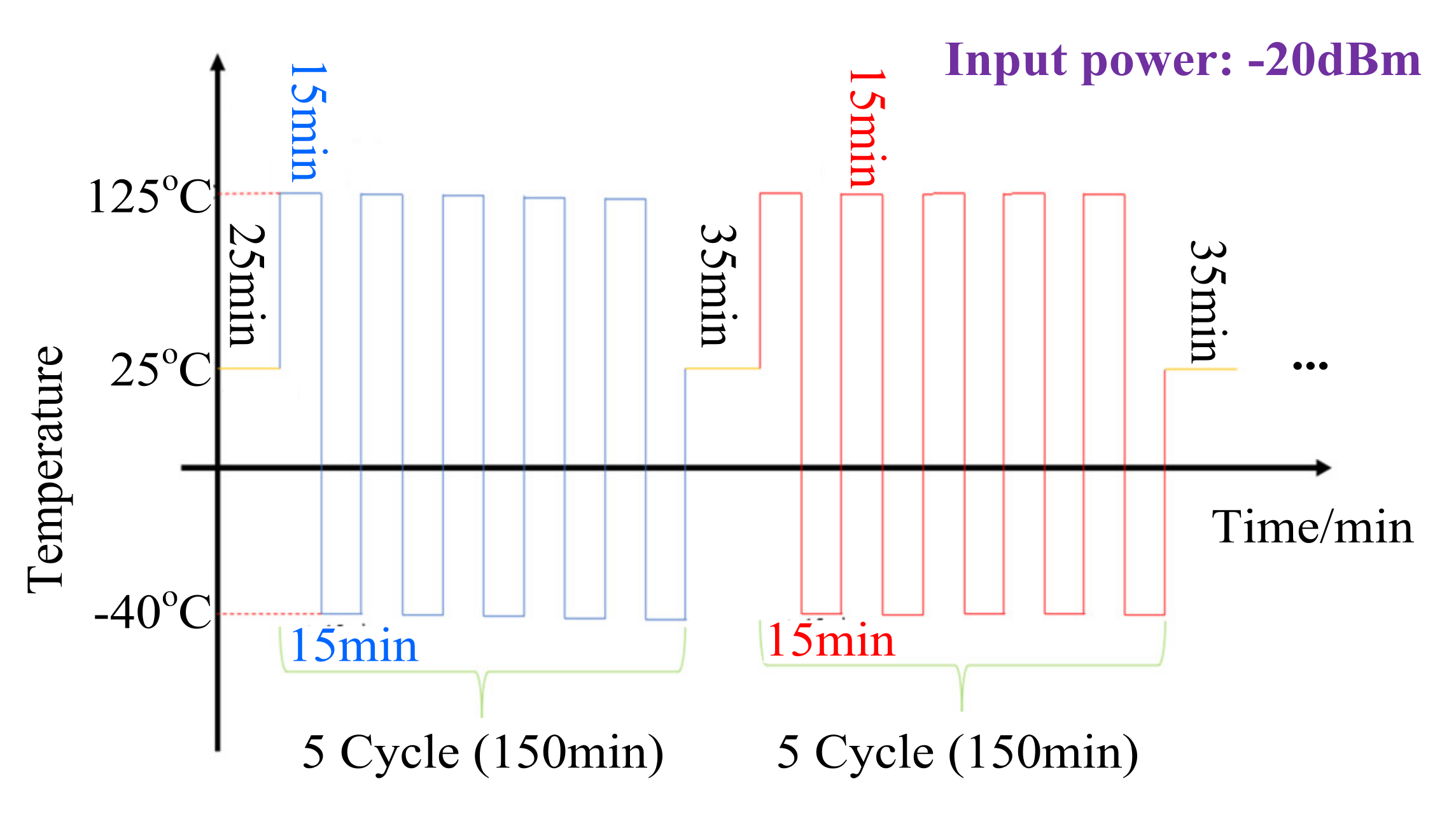
2.2. Thermal-Shock Test
3. Results and Discussions
3.1. DC Current
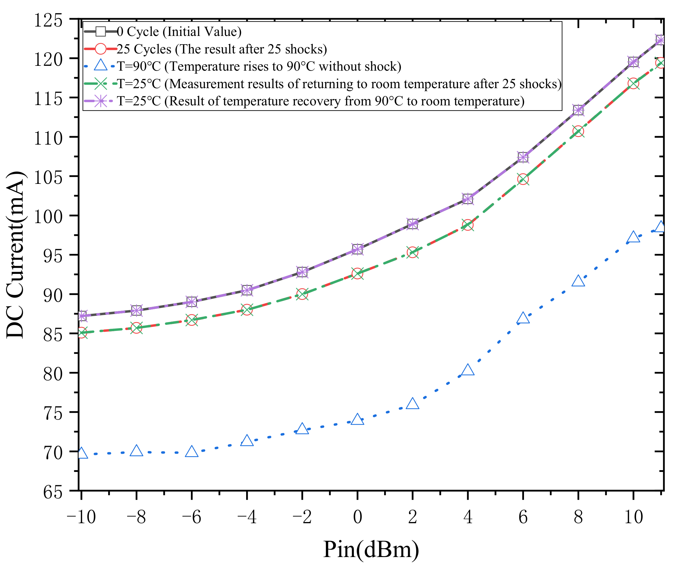
3.1.1. Thermal Shock Experiment
3.1.2. Typical Temperature Experiment
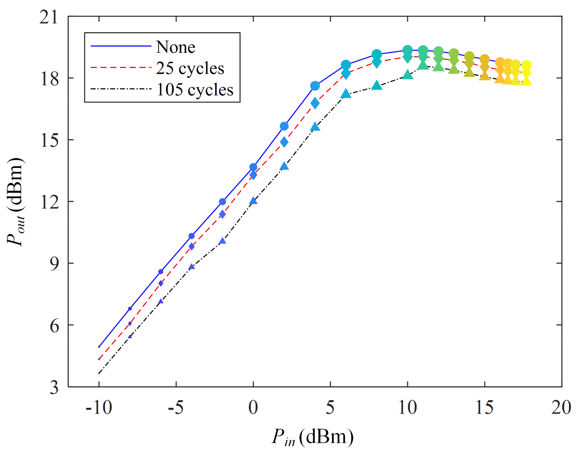
3.2. Output Power
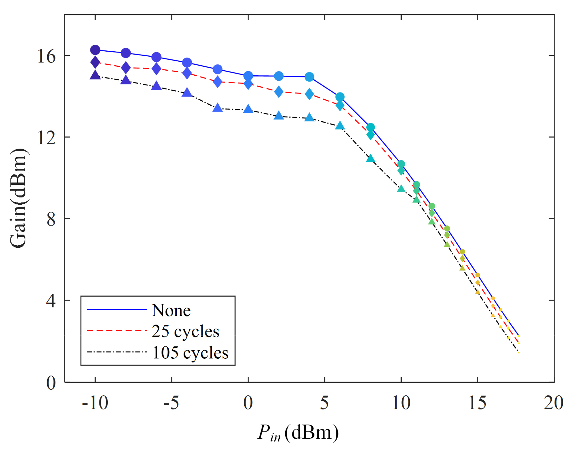
3.3. Gain
3.4. Power-Added Efficiency
4. Discussion and Conclusions
Author Contributions
Funding
Conflicts of Interest
References
- Moreno Rubio, J.J.; Angarita Malaver, E.F.; Lara González, L.Á. Wideband Doherty Power Amplifier: A Design Approach. Micromachines 2022, 13, 497. [Google Scholar] [CrossRef] [PubMed]
- Balani, W.; Sarvagya, M.; Ali, T.; Samasgikar, A.; Kumar, P.; Pathan, S.; Pai, M.M.M. A 20–44 GHz Wideband LNA Design Using the SiGe Technology for 5G Millimeter-Wave Applications. Micromachines 2021, 12, 1520. [Google Scholar] [CrossRef] [PubMed]
- Raymond, S.P.; Simon, M.W.; James, W.M.; Scott, T.S.; William, L.P. A review of GaN on SiC high electron-mobility power transistors and MMICs. IEEE Trans. Microw. Theory Tech. 2012, 60, 1764–1783. [Google Scholar]
- Yang, C.; Feng, F. Multi-Step-Ahead Prediction for a CMOS Low Noise Amplifier Aging Due to NBTI and HCI Using Neural Networks. J. Electro. Test. 2019, 35, 797–808. [Google Scholar] [CrossRef]
- Vittorio, G.; Egidio, R.; Giuseppe, P. A 15-dBm SiGe BiCMOS PA for 77-GHz Automotive Radar. IEEE Trans. Microw. Theory Tech. 2011, 59, 2910–2918. [Google Scholar]
- Seunghoon, K.; Donghyun, B.; Songcheol, H. A 5-GHz WLAN RF CMOS power amplifier with a parallel cascaded configuration and an active feedback linearizer. IEEE Trans. Microw. Theory Tech. 2019, 65, 3230–3244. [Google Scholar]
- Lin, Q.; Wu, H.; Li, X. Study of temperature reliability for a parallel high-efficiency class-E power amplifier. Cir. World 2017, 43, 111–117. [Google Scholar] [CrossRef]
- Gashi, B.; Krause, S.; Rüdiger, Q.; Fager, C.; Ambacher, O. Investigations of Active Antenna Doherty Power Amplifier Modules Under Beam-Steering Mismatch. IEEE Microw. Wirel. Compon. Lett. 2018, 28, 930–932. [Google Scholar] [CrossRef]
- Lin, X.; Seet, B.; Joseph, F. Wearable humidity sensing antenna for BAN applications over 5G networks. In Proceedings of the 2018 IEEE 19th Wireless and Microwave Technology Conference (WAMICON), Sand Key, FL, USA, 8–9 April 2018. [Google Scholar]
- Zhou, S.H.; Fu, H.P.; Ma, J.G.; Zhou, Q.J. A Neural Network Modeling Approach to Power amplifiers Taking into Account Temperature Effects. In Proceedings of the 2018 IEEE/MTT-S International Microwave Symposium-IMS, Philadelphia, PA, USA, 10–15 June 2018. [Google Scholar]
- Lin, Y.C.; Zhong, J. A review of the influencing factors on anisotropic conductive adhesives joining technology in electrical applications. J. Mater. Sci. 2008, 43, 3072–3093. [Google Scholar] [CrossRef]
- Talking about the ‘Shelf Life’ of Missiles. Available online: http://www.81.cn/jfjbmap/content/2018-03/09/content_201251.htm (accessed on 9 March 2018).
- Lin, Q.; Fu, H.P.; Cheng, Q.F.; Zhu, Y.Y. Study of the index failure for power amplifier caused by temperature. Analog Int. Circuits Signal Proc. 2016, 89, 177–183. [Google Scholar] [CrossRef]
- Kim, Y.T.; Kim, K.B.; Hyun, Y.E.; Kim, I.J.; Yang, S. Simulation study on the lifetime of electrochemical capacitors using the accelerated degradation test under temperature and voltage stresses. Microelectr. Reliab. 2015, 55, 2712–2720. [Google Scholar] [CrossRef]
- Shrivastava, A.A.; Azarian, M.H.; Pecht, M. Failure of Polymer Aluminum Electrolytic Capacitors Under Elevated Temperature Humidity Environments. IEEE Trans. Comp. Pack. Manufac. Tech. 2017, 7, 745–750. [Google Scholar] [CrossRef]
- Zhang, H. Reliability and lifetime prediction of LED drivers. In Proceedings of the 2017 14th China International Forum on Solid State Lighting: International Forum on Wide Bandgap Semiconductors China (SSLChina: IFWS), Beijing, China, 1–3 November 2017. [Google Scholar]
- Zhao, D.X.; Patrick, R. A 60-GHz dual-mode class AB power amplifier in 40-nm CMOS. IEEE J. Solid-State Circuits 2013, 48, 2323–2337. [Google Scholar] [CrossRef]
- Wu, H.F.; Wang, L.G.; Zhou, P.; Ma, J.G. A 0.1–1.2 GHz CMOS ultra-broadband power amplifier. In Proceedings of the 2014 IEEE MTT-S International Microwave Symposium (IMS2014), Tampa, FL, USA,, 1–4, June 2014. [Google Scholar]
- Neamen, D.A. Semiconductor Physics and Devices: Basic Principles; McGraw-Hill: New York, NY, USA, 2011; pp. 387–410. [Google Scholar]
- Casady, J.B.; Hull, B.; Zhangy, J.; Gajewski, D.; Wang, G.; Allen, S. First automotive reliability assessment and drive-train performance of large-area 900V, 10mOhm SiC MOSFETs. In Proceedings of the 2017 IEEE Applied Power Electronics Conference and Exposition (APEC), Tampa, FL, USA, 26–30 March 2017; pp. 2259–2262. [Google Scholar]
- Zhou, S.H.; Wang, J. An RF Stress-Based Thermal Shock Test Method for a CMOS Power Amplifier. IEEE J. Electron. Devices Soc. 2021, 9, 1024–1029. [Google Scholar] [CrossRef]
- Gray, P.R.; Hurst, P.J.; Lewis, S.H.; Meyer, R.G. Analysis and Design of Analog Integrated Circuits; Wiley: Hoboken, NJ, USA, 2001. [Google Scholar]
- Jiang, C.; Hu, C.; Chen, C.H.; Tseng, P.N. Impact of inter-metal-oxide deposition condition on NMOS and PMOS transistor hot carrier effect. In Proceedings of the 30th Annual Proceedings Reliability Physics, San Diego, CA, USA, 1 February 1992. [Google Scholar]

Publisher’s Note: MDPI stays neutral with regard to jurisdictional claims in published maps and institutional affiliations. |
© 2022 by the authors. Licensee MDPI, Basel, Switzerland. This article is an open access article distributed under the terms and conditions of the Creative Commons Attribution (CC BY) license (https://creativecommons.org/licenses/by/4.0/).
Share and Cite
Zhou, S.; Yang, C.; Wang, J. Investigation of the Specification Degradation Mechanism of CMOS Power Amplifier under Thermal Shock Test. Micromachines 2022, 13, 815. https://doi.org/10.3390/mi13060815
Zhou S, Yang C, Wang J. Investigation of the Specification Degradation Mechanism of CMOS Power Amplifier under Thermal Shock Test. Micromachines. 2022; 13(6):815. https://doi.org/10.3390/mi13060815
Chicago/Turabian StyleZhou, Shaohua, Cheng Yang, and Jian Wang. 2022. "Investigation of the Specification Degradation Mechanism of CMOS Power Amplifier under Thermal Shock Test" Micromachines 13, no. 6: 815. https://doi.org/10.3390/mi13060815
APA StyleZhou, S., Yang, C., & Wang, J. (2022). Investigation of the Specification Degradation Mechanism of CMOS Power Amplifier under Thermal Shock Test. Micromachines, 13(6), 815. https://doi.org/10.3390/mi13060815