Article

An Experimental and Systematic Insight into the Temperature Sensitivity for a 0.15-µm Gate-Length HEMT Based on the GaN Technology

by
Mohammad Abdul Alim
1,
Christophe Gaquiere
2 and
Giovanni Crupi
3,*
1
Department of Electrical and Electronic Engineering, University of Chittagong, Chittagong 4331, Bangladesh
2
Institute of Electronic, Microelectronic and Nanotechnology (IEMN), The University of Lille, F-59000 Lille, France
3
Department of Biomedical and Dental Sciences and Morphofunctional Imaging, University of Messina, 98125 Messina, Italy
*
Author to whom correspondence should be addressed.
Micromachines 2021, 12(5), 549; https://doi.org/10.3390/mi12050549
Submission received: 26 April 2021 / Revised: 7 May 2021 / Accepted: 11 May 2021 / Published: 12 May 2021

Abstract

:
Presently, growing attention is being given to the analysis of the impact of the ambient temperature on the GaN HEMT performance. The present article is aimed at investigating both DC and microwave characteristics of a GaN-based HEMT versus the ambient temperature using measured data, an equivalent-circuit model, and a sensitivity-based analysis. The tested device is a 0.15-μm ultra-short gate-length AlGaN/GaN HEMT with a gate width of 200 μm. The interdigitated layout of this device is based on four fingers, each with a length of 50 μm. The scattering parameters are measured from 45 MHz to 50 GHz with the ambient temperature varied from −40 °C to 150 °C. A systematic study of the temperature-dependent performance is carried out by means of a sensitivity-based analysis. The achieved findings show that by the heating the transistor, the DC and microwave performance are degraded, due to the degradation in the electron transport properties.

1. Introduction

As well-known, high electron-mobility transistors (HEMTs) based on the aluminum gallium nitride/gallium nitride (AlGaN/GaN) heterojunction are outstanding candidates for high-frequency, high-power, and high-temperature applications, owing to the unique physical properties of the GaN material. Throughout the years, many studies have been dedicated to the investigation of how the temperature impacts the performance of GaN-based HEMT devices. To this end, both electro-thermal simulations [1,2,3,4,5,6] and measurement-based analysis [7,8,9,10,11,12,13,14,15,16,17,18,19,20,21,22,23,24,25,26] have been developed. Although the electro-thermal device simulation is undoubtedly a very powerful and costless tool to deeply understand the underlying physics behind the operation of the transistor in order to improve the device fabrication, the measurement-based investigation is a step of crucial importance for achieving a reliable validation of a transistor technology prior to its use in real applications. Typically, measurements are coupled with the extraction of a small-signal equivalent-circuit model, which can be used as cornerstone for building both large-signal [27,28,29] and noise [30,31,32] transistor models that are essential for a successful design of microwave high-power [33,34,35,36] and low-noise amplifiers [36,37,38]. Compared to the effective modeling approach based on using artificial neural networks (ANNs) [39,40], the equivalent-circuit model allows a physically meaningful description [41,42,43], thereby enabling development of a sensitivity-based investigation.
To gain a comprehensive insight, the present article focuses on the impact of the ambient temperature (Ta) on the behavior of an on-wafer GaN HEMT using DC and microwave measurements coupled with a small-signal equivalent-circuit model and a sensitivity-based analysis. The device under test (DUT) is an ultra-short gate-length HEMT based on an AlGaN/GaN heterojunction grown on a silicon carbide (SiC) substrate. The DUT has a gate length of 0.15 μm and a gate width of 200 μm. The interdigitated layout consists of four fingers, each being 50-μm long. The DC characteristics and the scattering parameters from 45 MHz to 50 GHz are measured at nine different ambient temperature conditions by both cooling and heating the device, spanning the −40 °C to 150 °C temperature range. The measured data are used for equivalent-circuit extraction and sensitivity-based analysis, enabling one to assess the impact of the variation in the ambient temperature on the transistor performance. Basically, the main goal of this work is to extend the results of a previous article focused on the same DUT [15] by developing a sensitivity-based analysis, thus enabling a quantitative and systematic investigation of the effects of changes in the ambient temperature on the DC and microwave characteristics. Nevertheless, it should be pointed out that the obtained results are not of general validity, as they may strongly depend on the selected device and operating bias condition.
The paper is structured with the following sections. Section 2 describes the DUT and the experimental characterization, Section 3 reports and discusses the achieved findings, and Section 4 presents the conclusions.

2. Device under Test and Experimental Details

The metal organic chemical vapor deposition (MOCVD) technique is used to grow the Al0.253Ga0.747N/GaN heterostructure on a 400-μm-thick SiC substrate. The schematic cross-sectional view and the photograph of the tested GaN HEMT are illustrated in Figure 1. The epitaxial layer structure of the device is made up of a 25-nm-thick undoped (UD) AlGaN barrier and a 1.5-μm-thick UD GaN buffer layer. A 300-nm-thick graded AlN relaxation layer was grown between the GaN buffer and the SiC substrate. The device was capped with a 5-nm-tick n+-GaN layer. The evaporation process was employed to create the source and drain ohmic contacts (Ti/Al/Ni/Au with thicknesses of 12/200/40/100 nm, respectively) and followed by 30 s of thermal annealing at 900 °C. The Schottky mushroom-shaped gate was formed through Pt/Ti/Pt/Au evaporation and the subsequent lift-off process. Finally, a Si3N4 layer with a thickness of 240 nm was deposited to passivate the device. The gate length of the tested GaN device is 0.15 μm. The interdigitated architecture of the device is based on the parallel connection of four 50-μm long fingers, resulting in a total gate width of 200 μm. The source-to-gate distance (LSG) and the gate-to-drain distance (LGD) are 1 μm and 2.85 μm, respectively. The DUT was fabricated at the University of Lille, France.
The microwave experiments consist of DC and S-parameters measured from 45 MHz to 50 GHz at nine different ambient temperatures: −40 °C, −25 °C, 0 °C, 25 °C, 50 °C, 75 °C, 100 °C, 125 °C, and 150 °C. The analysis is performed using the DC characteristics and the S-parameters at a bias point in the saturation region: Vds = 15 and Vgs = −5 V. The device parameters were measured with a thermal probe station connected to an HP8510C vector network analyzer (VNA) and with the aid of commercially available software to guarantee that the data are free of human error. The DC and frequency-dependent measurements were performed at each temperature after the sample reached uniform steady-state temperature. Figure 2 shows the measurement process, model extraction, and sensitivity-based analysis.

3. Experimental Results and Systematic Analysis

The systematic sensitivity-based analysis at the selected bias voltages is accomplished using the dimensionless relative sensitivity of each parameter (RSP) with respect to Ta, which is calculated by normalizing the relative change in P to the relative change in Ta:
R S P = Δ P P 0 T a 0 Δ T a = ( P P 0 ) P 0 T a 0 ( T a T a 0 )
where P0 is the value of the selected parameter P at the reference temperature (Ta0) of 25 °C.
The remainder of this section is divided into two subsections: the first part is focused on the impact of the ambient temperature on the DC characteristics, whereas the second part is dedicated to the effects of the variations in the ambient temperature on the microwave performance.

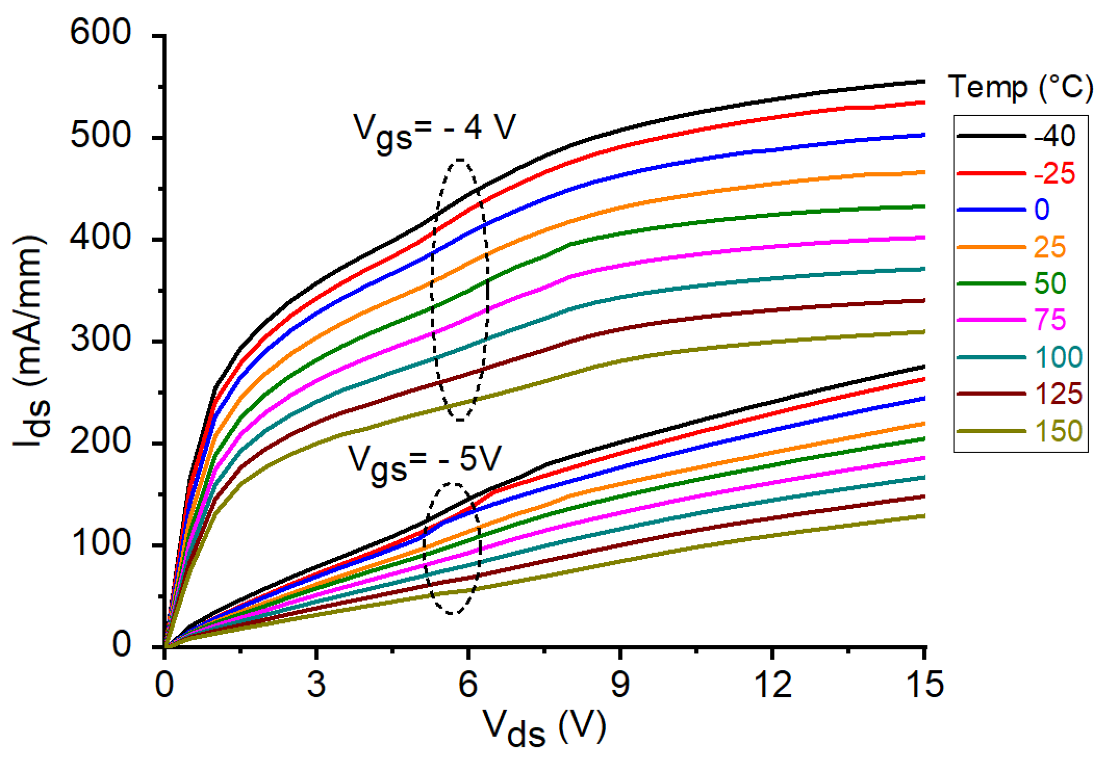
3.1. Sensitivity-Based Analysis of DC Characteristics

The DC output characteristics for the tested GaN HEMT at Vgs = −4 V and −5 V under different temperature conditions are illustrated in Figure 3. As can be clearly observed, Ids is considerably reduced with increasing temperature. This might be attributed to the degradation in the carrier transport properties as a consequence of the enhancement of the phonon-scattering processes at higher temperatures. Analogously, the reduction in Ids at higher temperatures can be observed by plotting the DC transcharacteristics of the studied device at Vds = 15 V (see Figure 4). Similar fashion of degradation can be seen in the transconductance by plotting the gm-Vgs curves at Vds = 15 V (see Figure 5a). As a matter of the fact, by heating the device, the transconductance is significantly reduced. However, it should be underlined that a higher temperature leads to a wider and flatter curve of gm versus Vgs, thus implying a better linearity. Over the years, many studies have been devoted at improving the flatness of gm versus Vgs, in order to yield to an improved transistor linearity and then to a more linear power amplifier [44,45]. For the sake of completeness, the behavior of gm is plotted also as a function of Ids (see Figure 5b). At the selected bias point: Vds = 15 V and Vgs = −5 V, both Ids and gm are significantly degraded when the temperature is raised, as illustrated in Figure 6a. The interesting feature found in the gm−Vgs curves of Figure 5a is that, by heating the device, the peak value of gm is not only greatly reduced but also shifted toward less negative values of Vgs. As shown in Figure 6b, the value of Vgs at which the peak in gm occurs (Vgm) is increased from −5.2 V at −40 °C to −4.8 V at 150 °C. It is worth noting that also the threshold voltage (Vth) shifts toward less negative values at higher Ta. As illustrated in Figure 6b, Vth is increased from −6.24 V at −40 °C to −5.64 V at 150 °C.
Using Equation (1), the relative sensitivities of Ids, gm, Vgm, and Vth with respect to Ta are calculated and reported in Figure 7. As can be observed, RSIds, RSgm, RSVth, and RSVgm are negative for the studied device, as a consequence of the fact that an increase in Ta leads to a reduction in the values of Ids, gm, Vth, and Vgm.

3.2. Sensitivity-Based Analysis of Small-Signal Parameters and RF Figures of Merit

The equivalent-circuit model in Figure 8 was used to model the measured S-parameters of the studied device. The equivalent-circuit parameters (ECPs) were extracted as described in [15], using the well-known “cold” pinch-off approach that has been widely and successfully applied to the GaN technology over the years [46,47,48,49,50]. The effect of Ta on the measured S-parameters at the selected bias point is shown in Figure 9. It should be highlighted that as the carrier transport properties deteriorate with increasing Ta, the low-frequency magnitude of S21 is reduced. This is in line with the degradation of the DC gm at higher Ta (see Figure 5). As can be observed, the tested device is affected by the kink effect in S22. As well-known, the GaN HEMT technology is prone to be affected by this phenomenon, owing to the relatively high transconductance [51,52,53,54]. In accordance with this, the observed kink effect in S22 is more pronounced at lower Ta, due to the higher gm. The DC parameters, ECPs, intrinsic input and feedback time constants (i.e., τgs = RgsCgs and τgd = RgdCgd), the unity current gain cut-off frequency (ft), and the maximum frequency of oscillation (fmax) are reported at 25 °C in Table 1. The three intrinsic time constants (τm, τgs, and τgd), which emerge from the inertia of the intrinsic transistor in reacting to rapid signal changes, are meant to represent the intrinsic non-quasi-static (NQS) effects, which play a more significant role at higher frequencies. The values of ft and fmax are obtained from the frequency-dependent behavior of the measured short-circuit current gain (h21) and maximum stable/available gain (MSG/MAG), respectively (see Figure 10).
Similarly, to what was done for the DC parameters, the relative sensitivities of the other parameters in Table 1 are calculated using equation 1 and then shown in Figure 11. Because of their low dependence on the temperature, the relative sensitivities of the extrinsic capacitances and inductances are almost nil, as depicted in Figure 11a,b. It can be observed in Figure 11c–e that the relative sensitivities of the extrinsic and intrinsic resistances are positive, reflecting the fact that the resistive contributions increase at higher temperatures. Figure 11f illustrates that unlike the resistances, the transconductance has a negative relative sensitivity, as this parameter is degraded when heating the device.
As illustrated in Figure 11d, the relative sensitivity of Cgs is negative, while the relative sensitivities of Cgd and Cds are positive. Figure 11g shows that the relative sensitivities of the intrinsic time constants are positive, indicating that they increase when the temperature is raised. This finding implies that the NQS effects occur at lower frequencies when the device is heated. As can be observed in Figure 11f, the relative sensitivities of ft and fmax are negative, implying lower operating frequencies at higher temperatures. Figure 11h shows that the relative sensitivities of the magnitude of S21 and h21 at 45 MHz are negative, in line with the reduction of the transconductance at higher temperatures, while the stability factor (K) shows a positive temperature sensitivity as illustrated at 1 GHz.
For the tested device, a good agreement between measured and simulated S-parameters was achieved. As an example, Figure 12 depicts the comparison between measurements and S-parameter simulations at two different Ta for the tested GaN HEMT at the selected bias condition. The simulations are obtained using the equivalent-circuit model depicted in Figure 8 by means of the commercial microwave simulation software advanced design system (ADS). The small-signal ECPs extracted for different Ta from the measured S-parameters are used as inputs to the schematic.

4. Conclusions

We have reported an experimental investigation on the impact of the ambient temperature on the DC and microwave performance of a transistor based on an ultra-short 0.15-μm GaN HEMT technology. Measurements have been coupled with an equivalent-circuit model and a sensitivity-based study to assess the thermal effects on device performance over the wide temperature range going from −40 °C to 150 °C. The relative sensitivity was used as the evaluation indicator for this study because it enables investigation of the effects of the ambient temperature on the device performance in a quantitative, systematic, and simple way. The measurement-based findings show that both DC and microwave performance of the studied device are remarkably degraded with increasing temperature.

Author Contributions

Conceptualization, M.A.A. and G.C.; methodology, M.A.A. and G.C.; validation, M.A.A.; investigation, M.A.A.; writing—original draft preparation, M.A.A. and G.C.; writing—review and editing, C.G. and G.C.; supervision, C.G. and G.C. All authors have read and agreed to the published version of the manuscript.

Funding

This research received no external funding.

Institutional Review Board Statement

Not applicable.

Informed Consent Statement

Not applicable.

Data Availability Statement

The data presented in this study are available on request from the authors.

Conflicts of Interest

The authors declare no conflict of interest. The funders had no role in the design of the study; in the collection, analyses, or interpretation of data; in the writing of the manuscript, or in the decision to publish the results.

References

  1. Heller, E.R.; Crespo, A. Electro-thermal modeling of multifinger AlGaN/GaN HEMT device operation including thermal substrate effects. Microelectron. Reliab. 2008, 48, 45–50. [Google Scholar] [CrossRef]
  2. Bertoluzza, F.; Delmonte, N.; Menozzi, R. Three-dimensional finite-element thermal simulation of GaN-based HEMTs. Microelectron. Reliab. 2009, 49, 468–473. [Google Scholar] [CrossRef]
  3. Zhang, Y.; Sun, M.; Liu, Z.; Piedra, D.; Lee, H.-S.; Gao, F.; Fujishima, T.; Palacios, T. Electrothermal Simulation and Thermal Performance Study of GaN Vertical and Lateral Power Transistors. IEEE Trans. Electron Devices 2013, 60, 2224–2230. [Google Scholar] [CrossRef]
  4. Chvála, A.; Marek, J.; Príbytný, P.; Šatka, A.; Donoval, M.; Donoval, D. Effective 3-D device electrothermal simulation analysis of influence of metallization geometry on multifinger power HEMTs properties. IEEE Trans. Electron Device 2017, 64, 333–336. [Google Scholar] [CrossRef]
  5. Gupta, M.P.; Vallabhaneni, A.K.; Kumar, S. Self-consistent electrothermal modeling of passive and microchannel cooling in AlGaN/GaN HEMTs. IEEE Trans. Compon. Packag. Manuf. Technol. 2017, 7, 1305–1312. [Google Scholar] [CrossRef]
  6. Hao, Q.; Zhao, H.; Xiao, Y.; Kronenfeld, M.B. Electrothermal studies of GaN-based high electron mobility transistors with improved thermal designs. Microelectron. Reliab. 2018, 116, 496–506. [Google Scholar] [CrossRef]
  7. Akita, M.; Kishimoto, S.; Mizutani, T. High-frequency measurements of AlGaN/GaN HEMTs at high temperatures. IEEE Electron. Device Lett. 2001, 22, 376–377. [Google Scholar] [CrossRef]
  8. Nuttinck, S.; Gebara, E.; Laskar, J.; Harris, H.M. Study of self-heating effects, temperature-dependent modeling, and pulsed load-pull measurements on GaN HEMTs. IEEE Trans. Microw. Theory Tech. 2001, 49, 2413–2420. [Google Scholar] [CrossRef]
  9. Lee, J.W.; Webb, K.J. A temperature-dependent nonlinear analytic model for AlGaN-GaN HEMTs on SiC. IEEE Trans. Microw. Theory Tech. 2004, 52, 2–9. [Google Scholar] [CrossRef]
  10. Thorsell, M.; Andersson, K.; Fagerlind, M.; Südow, M.; Nilsson, P.-A.; Rorsman, N. Thermal study of the high-frequency noise in GaN HEMTs. IEEE Trans. Microw. Theory Tech. 2009, 57, 19–26. [Google Scholar] [CrossRef]
  11. Darwish, A.M.; Huebschman, B.D.; Viveiros, E.; Hung, H.A. Dependence of GaN HEMT millimeter-wave performance on temperature. IEEE Trans. Microw. Theory Tech. 2009, 57, 3205–3211. [Google Scholar] [CrossRef]
  12. Darwish, A.M.; Ibrahim, A.A.; Hung, H.A. Temperature Dependence of GaN HEMT Small Signal Parameters. Int. J. Microw. Sci. Technol. 2011, 2011, 945189. [Google Scholar] [CrossRef] [Green Version]
  13. Marinković, Z.; Crupi, G.; Caddemi, A.; Avolio, G.; Raffo, A.; Marković, V.; Vannini, G.; Schreurs, D.M.M.-P. Neural approach for temperature-dependent modeling of GaN HEMTs. Int. J. Numer. Model. Electron. Netw. Devices Fields 2014, 28, 359–370. [Google Scholar] [CrossRef]
  14. Crupi, G.; Raffo, A.; Avolio, G.; Schreurs, D.M.M.-P.; Vannini, G.; Caddemi, A. Temperature influence on GaN HEMT equivalent circuit. IEEE Microw. Wirel. Comp. Lett. 2016, 26, 813–815. [Google Scholar] [CrossRef]
  15. Alim, M.A.; Rezazadeh, A.A.; Gaquiere, C. Temperature effect on DC and equivalent circuit parameters of 0.15-μm gate length GaN/SiC HEMT for microwave applications. IEEE Trans. Microw. Theory Tech. 2016, 64, 3483–3491. [Google Scholar] [CrossRef]
  16. Zhao, X.; Xu, Y.; Jia, Y.; Wu, Y.; Xu, R.; Li, J.; Hu, Z.; Wu, H.; Dai, W.; Cai, S. Temperature-Dependent Access Resistances in Large-Signal Modeling of Millimeter-Wave AlGaN/GaN HEMTs. IEEE Trans. Microw. Theory Tech. 2017, 65, 2271–2278. [Google Scholar] [CrossRef]
  17. Bouslama, M.; Gillet, V.; Chang, C.; Nallatamby, J.-C.; Sommet, R.; Prigent, M.; Quere, R.; Lambert, B. Dynamic Performance and Characterization of Traps Using Different Measurements Techniques for the New AlGaN/GaN HEMT of 0.15-µm Ultrashort Gate Length. IEEE Trans. Microw. Theory Tech. 2019, 67, 2475–2482. [Google Scholar] [CrossRef]
  18. Alim, M.A.; Hasan, M.A.; Rezazadeh, A.A.; Gaquiere, C.; Crupi, G. Multibias and temperature dependence of the current-gain peak in GaN HEMT. Int. J. RF Microw. Comput. Aided Eng. 2019, 30, e22129. [Google Scholar] [CrossRef]
  19. Crupi, G.; Raffo, A.; Vadalà, V.; Vannini, G.; Caddemi, A. High-periphery GaN HEMT modeling up to 65 GHz and 200 °C. Solid-State Electron. 2019, 152, 11–16. [Google Scholar] [CrossRef]
  20. Chen, Y.; Xu, Y.; Kong, Y.; Chen, T.; Zhang, Y.; Yan, B.; Xu, R. Temperature-dependent small signal performance of GaN-on-diamond HEMTs. Int. J. Numer. Model. Electron. Netw. Dev. Field 2020, 33, e2620. [Google Scholar] [CrossRef]
  21. Gryglewski, D.; Wojtasiak, W.; Kamińska, E.; Piotrowska, A. Characterization of self-heating process in GaN-based HEMTs. Electronics 2020, 9, 1305. [Google Scholar] [CrossRef]
  22. Majumdar, A.; Chatterjee, S.; Chatterjee, S.; Chaudhari, S.S.; Poddar, D.R. An ambient temperature dependent small signal model of GaN HEMT using method of curve fitting. Int. J. RF Microw. Comput. Aided Eng. 2020, 30, e22434. [Google Scholar] [CrossRef]
  23. Jarndal, A.; Husain, S.; Hashmi, M. Genetic algorithm initialized artificial neural network based temperature dependent small-signal modeling technique for GaN high electron mobility transistors. Int. J. RF Microw. Comput. Aided Eng. 2021, 31, e22542. [Google Scholar] [CrossRef]
  24. Luo, H.; Zhong, Z.; Hu, W.; Guo, Y. Analysis and modeling of the temperature-dependent nonlinearity of intrinsic capacitances in AlGaN/GaN HEMTs. IEEE Microw. Wirel. Comp. Lett. 2021, 31, 373–376. [Google Scholar] [CrossRef]
  25. Colangeli, S.; Ciccognani, W.; Longhi, P.E.; Pace, L.; Poulain, J.; Leblanc, R.; Limiti, E. Linear characterization and modeling of GaN-on-Si HEMT technologies with 100 nm and 60 nm gate lengths. Electronics 2021, 10, 134. [Google Scholar] [CrossRef]
  26. Jarndal, A.; Alim, M.A.; Raffo, A.; Crupi, G. 2-mm-gate-periphery GaN high electron mobility transistors on SiC and Si substrates: A comparative analysis from a small-signal standpoint. Int. J. RF Microw. Comput. Aided Eng. 2021, 31, e22642. [Google Scholar] [CrossRef]
  27. Root, D.E.; Hughes, B. Principles of nonlinear active device modeling for circuit simulation. In Proceedings of the 32nd ARFTG Conference Digest, Tempe, AZ, USA, 1–2 December 1988; pp. 1–24. [Google Scholar]
  28. Xu, Y.; Wang, C.; Sun, H.; Wen, Z.; Wu, Y.; Xu, R.; Yu, X.; Ren, C.; Wang, Z.; Zhang, B.; et al. A Scalable Large-Signal Multiharmonic Model of AlGaN/GaN HEMTs and Its Application in C-Band High Power Amplifier MMIC. IEEE Trans. Microw. Theory Tech. 2017, 65, 2836–2846. [Google Scholar] [CrossRef]
  29. Raffo, A.; Avolio, G.; Vadalà, V.; Schreurs, D.M.M.-P.; Vannini, G. A non-quasi-static FET model extraction procedure using the dynamic-bias technique. IEEE Microw. Wirel. Comp. Lett. 2015, 25, 841–843. [Google Scholar] [CrossRef]
  30. Lee, S.; Webb, K.J.; Tialk, V.; Eastman, L.F. Intrinsic noise equivalent-circuit parameters for AlGaN/GaN HEMTs. IEEE Trans Microw. Theory Tech. 2003, 51, 1567–1577. [Google Scholar]
  31. Pace, L.; Colangeli, S.; Ciccognani, W.; Longhi, P.E.; Limiti, E.; Leblanc, R.; Feudale, M.; Vitobello, F. Design and validation of 100 nm GaN-On-Si Ka-band LNA based on custom noise and small signal models. Electronics 2020, 9, 150. [Google Scholar] [CrossRef] [Green Version]
  32. Jarndal, A.; Hussein, A.; Crupi, G.; Caddemi, A. Reliable noise modeling of GaN HEMTs for designing low-noise amplifiers. Int. J. Numer. Model. Electron. Netw. Dev. Field 2020, 33, e2585. [Google Scholar] [CrossRef]
  33. Cabral, P.M.; Pedro, J.C.; Carvalho, N.B. Nonlinear device model of microwave power GaN HEMTs for high power-amplifier design. IEEE Trans. Microw. Theory Tech. 2004, 52, 2585–2592. [Google Scholar] [CrossRef]
  34. Raffo, A.; Scappaviva, F.; Vannini, G. A new approach to microwave power amplifier design based on the experimental characterization of the intrinsic electron-device load line. IEEE Trans. Microw. Theory Tech. 2009, 57, 1743–1752. [Google Scholar] [CrossRef]
  35. Kim, S.; Lee, M.-P.; Hong, S.-J.; Kim, D.-W. Ku-Band 50 W GaN HEMT power amplifier using asymmetric power combining of transistor cells. Micromachines 2018, 9, 619. [Google Scholar] [CrossRef] [Green Version]
  36. Crupi, G.; Vadalà, V.; Colantonio, P.; Cipriani, E.; Caddemi, A.; Vannini, G.; Schreurs, D.M.M.-P. Empowering GaN HEMT models: The gateway for power amplifier design. Int. J. Numer. Model. Electron. Netw. Devices Fields 2015, 30, e2125. [Google Scholar] [CrossRef]
  37. Colangeli, S.; Bentini, A.; Ciccognani, W.; Limiti, E.; Nanni, A. GaN-based robust low-noise amplifiers. IEEE Trans. Electron Dev. 2013, 60, 3238–3248. [Google Scholar] [CrossRef]
  38. Nalli, A.; Raffo, A.; Crupi, G.; D’Angelo, S.; Resca, D.; Scappaviva, F.; Salvo, G.; Caddemi, A.; Vannini, G. GaN HEMT Noise Model Based on Electromagnetic Simulations. IEEE Trans. Microw. Theory Tech. 2015, 63, 2498–2508. [Google Scholar] [CrossRef]
  39. Marinković, Z.; Crupi, G.; Caddemi, A.; Markovic, V.; Schreurs, D.M.M.-P. A review on the artificial neural network applications for small-signal modeling of microwave FETs. Int. J. Numer. Model. Electron. Netw. Dev. Field 2020, 33, e2668. [Google Scholar] [CrossRef]
  40. Jin, J.; Feng, F.; Na, W.C.; Yan, S.X.; Liu, W.Y.; Zhu, L.; Zhang, Q.J. Recent advances in neural network-based inverse modeling techniques for microwave applications. Int. J. Numer. Model. Electron. Netw. Dev. Field 2020, 33, e2732. [Google Scholar] [CrossRef]
  41. Dambrine, G.; Cappy, A.; Heliodore, F.; Playez, E. A new method for determining the FET small-signal equivalent circuit. IEEE Trans Microw. Theory Tech. 1988, 36, 1151–1159. [Google Scholar] [CrossRef]
  42. Alt, R.; Marti, D.; Bolognesi, C.R. Transistor modeling: Robust small-signal equivalent circuit extraction in various HEMT technologies. IEEE Microw. Mag. 2013, 14, 83–101. [Google Scholar] [CrossRef]
  43. Crupi, G.; Caddemi, A.; Schreurs, D.M.M.-P.; Dambrine, G. The large world of FET small-signal equivalent circuits. Int. J. RF Microw. Comput. Aided Eng. 2016, 26, 749–762. [Google Scholar] [CrossRef]
  44. Chen, C.-H.; Sadler, R.; Wang, D.; Hou, D.; Yang, Y.; Yau, W.; Sutton, W.; Shim, J.; Wang, S.; Duong, A. The causes of GaN HEMT bell-shaped transconductance degradation. Solid-State Electron. 2016, 126, 115–124. [Google Scholar] [CrossRef]
  45. Ancona, M.G.; Calame, J.P.; Meyer, D.J.; Rajan, S.; Downey, B.P. Compositionally graded III-N HEMTs for improved linearity: A simulation study. IEEE Trans. Electron Device 2019, 66, 2151–2157. [Google Scholar] [CrossRef]
  46. Jarndal, A.; Kompa, G. A new small signal modeling approach applied to GaN devices. IEEE Trans. Microw. Theory Tech. 2005, 53, 3440–3448. [Google Scholar] [CrossRef]
  47. Brady, R.G.; Oxley, C.H.; Brazil, T.J. An improved small-signal parameter-extraction algorithm for GaN HEMT devices. IEEE Trans. Microw. Theory Tech. 2008, 56, 1535–1544. [Google Scholar] [CrossRef]
  48. Al Sabbagh, M.; Yagoub, M.C.E.; Park, J. New small-signal extraction method applied to GaN HEMTs on different substrates. Int. J. R. F. Microw. Comput. Aided Eng. 2020, 30, e22291. [Google Scholar] [CrossRef]
  49. Chen, Y.; Xu, Y.; Luo, Y.; Wang, C.; Wen, Z.; Yan, B.; Xu, R. A reliable and efficient small-signal parameter extraction method for GaN HEMTs. Int. J. Numer. Model. Electron. Netw. Dev. Field 2020, 33, e2540. [Google Scholar] [CrossRef]
  50. Du, X.; Helaoui, M.; Cai, J.; Liu, J.; Ghannouchi, F.M. Improved small-signal hybrid parameter-extraction technique for AlGaN/GaN high electron mobility transistors. Int. J. RF Microw. Comput. Aided Eng. 2021, 31, e22562. [Google Scholar] [CrossRef]
  51. Crupi, G.; Raffo, A.; Marinkovic, Z.; Avolio, G.; Caddemi, A.; Markovic, V.; Vannini, G.; Schreurs, D.M.M.-P. An Extensive Experimental Analysis of the Kink Effects in S22 and h21 for a GaN HEMT. IEEE Trans. Microw. Theory Tech. 2014, 62, 513–520. [Google Scholar] [CrossRef]
  52. Ahsan, S.A.; Ghosh, S.; Khandelwal, S.; Chauhan, Y.S. Modeling of kink-effect in RF behaviour of GaN HEMTs using ASM-HEMT model. In Proceedings of the IEEE International Conference Electron Devices Solid-State Circuits, Hong Kong, China, 3–5 August 2016; pp. 426–429. [Google Scholar] [CrossRef]
  53. Alim, M.A.; Hasan, M.A.; Rezazadeh, A.A.; Gaquiere, C.; Crupi, G. Thermal influence on S22 kink behavior of a 0.15-μm gate length AlGaN/GaN/SiC HEMT for microwave applications. Semicond. Sci. Technol. 2019, 34, 1–8. [Google Scholar] [CrossRef]
  54. Crupi, G.; Raffo, A.; Vadalà, V.; Vannini, G.; Caddemi, A. A new study on the temperature and bias dependence of the kink effects in S22 and h21 for the GaN HEMT technology. Electronics 2018, 7, 353. [Google Scholar] [CrossRef] [Green Version]
Figure 1. (a) Schematic drawing of the epitaxial structure and (b) photograph of the tested 0.15 μm × (4 × 50) μm GaN HEMT.
Micromachines 12 00549 g001
Figure 2. The flow diagram of the measurement process, model extraction, and sensitivity-based analysis for the tested on-wafer GaN HEMT.
Micromachines 12 00549 g002
Figure 3. DC output characteristics of the studied GaN HEMT at Vgs = −4 V and −5 V under different temperature conditions.
Micromachines 12 00549 g003
Figure 4. DC transcharacteristics of the studied GaN HEMT at Vds = 15 V under different temperature conditions.
Micromachines 12 00549 g004
Figure 5. DC transconductance of the studied GaN HEMT at Vds = 15 V under different temperature conditions. The data are reported as a function of (a) Vgs and (b) Ids.
Micromachines 12 00549 g005
Figure 6. Temperature dependence of the DC parameters of the studied GaN HEMT: (a) Ids and gm at Vds = 15 V and Vgs = −5 V; (b) Vth and Vgm (i.e.,Vgs at which gm shows its peak value) at Vds = 15 V.
Micromachines 12 00549 g006
Figure 7. Temperature dependence of the relative sensitivities of the DC parameters of the studied GaN HEMT: (a) RSIds and RSgm at Vds = 15 V and Vgs = −5 V; (b) RSVth and RSVgm at Vds = 15 V.
Micromachines 12 00549 g007
Figure 8. The equivalent-circuit model for the GaN HEMT under investigation.
Micromachines 12 00549 g008
Figure 9. Measured S-parameters of the studied GaN HEMT at Vds = 15 V and Vgs = −5 V under different temperature conditions: (a) S11, S21, (b) S12, and S22.
Micromachines 12 00549 g009
Figure 10. Behavior of the magnitude of the h21 and MAG/MSG versus the frequency of the studied GaN HEMT at Vds = 15 V, Vgs = −5 V, and Ta = 25 °C.
Micromachines 12 00549 g010
Figure 11. The relative sensitivities of the analyzed parameters versus ambient temperature for the studied GaN HEMT: (a) RSCpg and RSCpd; (b) RSLg, RSLs, and RSLd; (c) RSRg, RSRs, and RSRd; (d) RSCgs, RSCgd, and RSCds; (e) RSRgs, RSRgd, and RSRds; (f) RSgmo, RSft, and RSfmax; (g) RSτm, RSτgs, and RSτgd; (h) RSS21 and RSh21 at 45 MHz and RSK at 1 GHz The illustrated bias points for intrinsic parameters and RF figures of merits is: Vds = 15 V and Vgs = −5 V.
Micromachines 12 00549 g011aMicromachines 12 00549 g011b
Figure 12. Measured (solid black lines) and simulated (dashed red lines) S-parameters from 45 MHz to 50 GHz for the studied GaN HEMT at 50 °C (a,b) and 125 °C (c,d). The illustrated bias point is: Vds = 15 V and Vgs = −5 V.
Micromachines 12 00549 g012
Table 1. Analyzed parameters for the studied GaN HEMTs at 25 °C for the bias condition of Vds = 15 V and Vgs = −5 V.
ParametersValueParametersValue
Ids (mA)44Cgs (fF)154
gm (mS)54Cgd (fF)28
Vth (V)−6Cds (fF)121
Vgm (V)−5.1Rgs (Ω)1.7
Cpg (fF)50Rgd (Ω)11.3
Cpd (fF)86Rds (Ω)225
Lg (pH)141gmo (mS)63
Ls (pH)1.8τm (ps)3.0
Ld (pH)63τgs (ps)1.6
Rg (Ω)2.7τgd (ps)2.0
Rs (Ω)3.0ft (GHz)47.3
Rd (Ω)5.8fmax (GHz)97
Publisher’s Note: MDPI stays neutral with regard to jurisdictional claims in published maps and institutional affiliations.

