Electrical Coupling and Simulation of Monolithic 3D Logic Circuits and Static Random Access Memory


Abstract
:1. Introduction
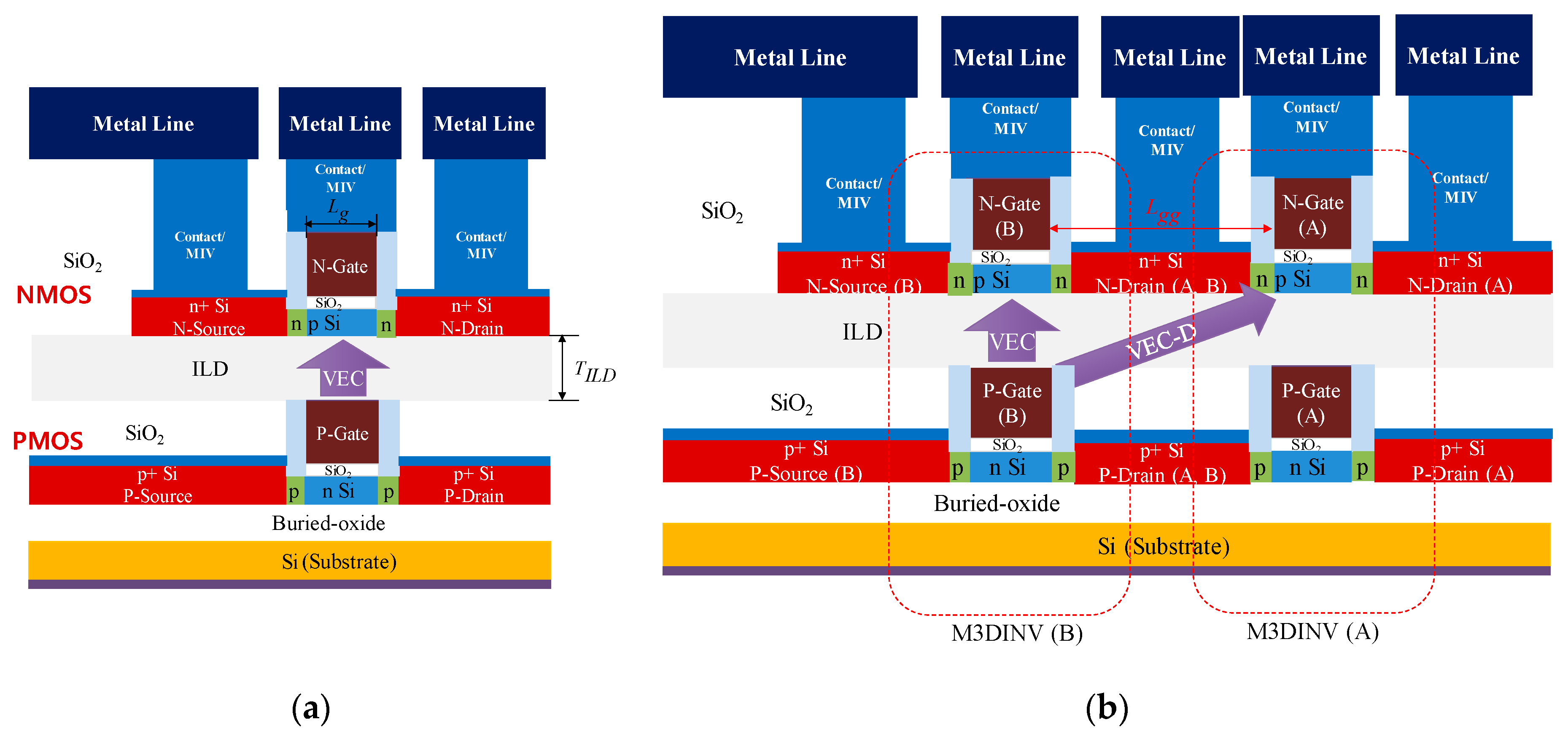
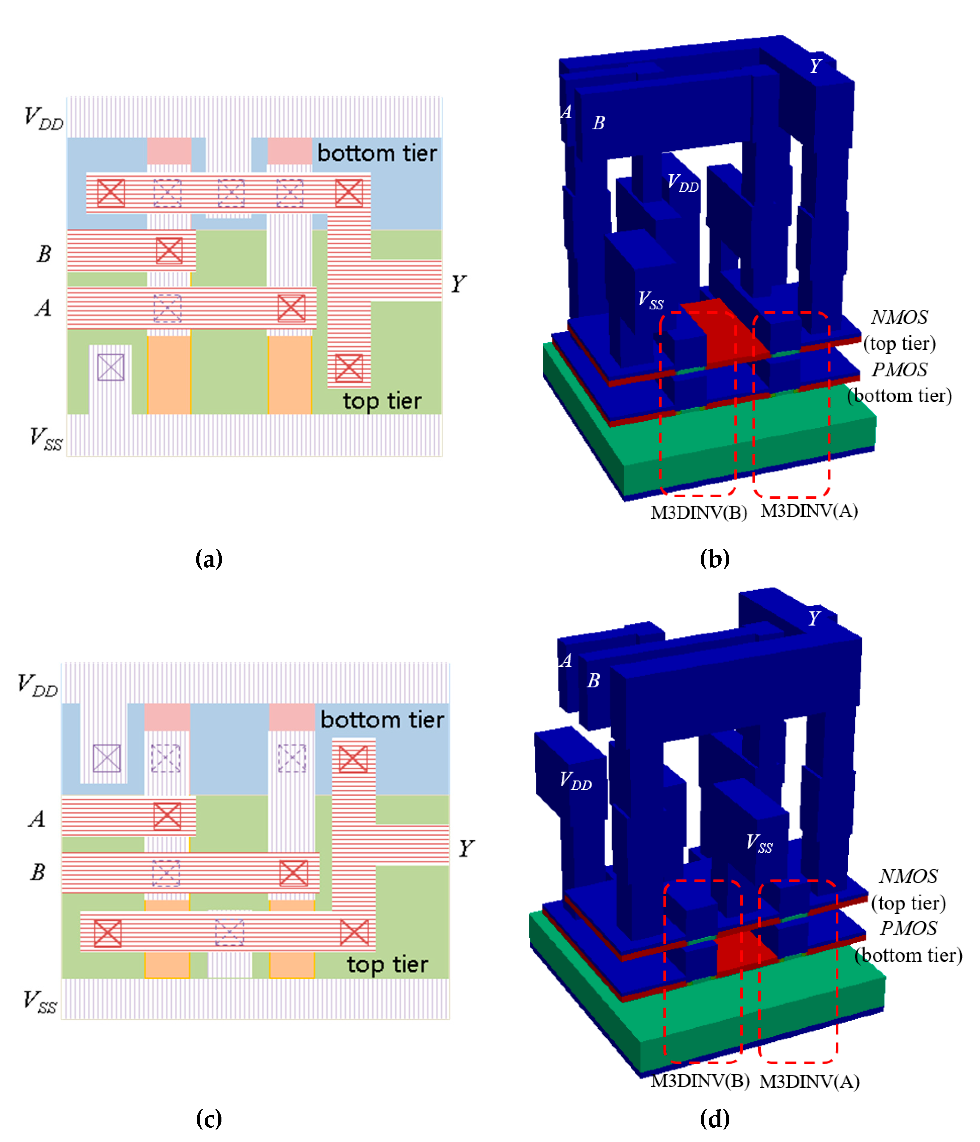
2. Structures
3. Electrical Coupling
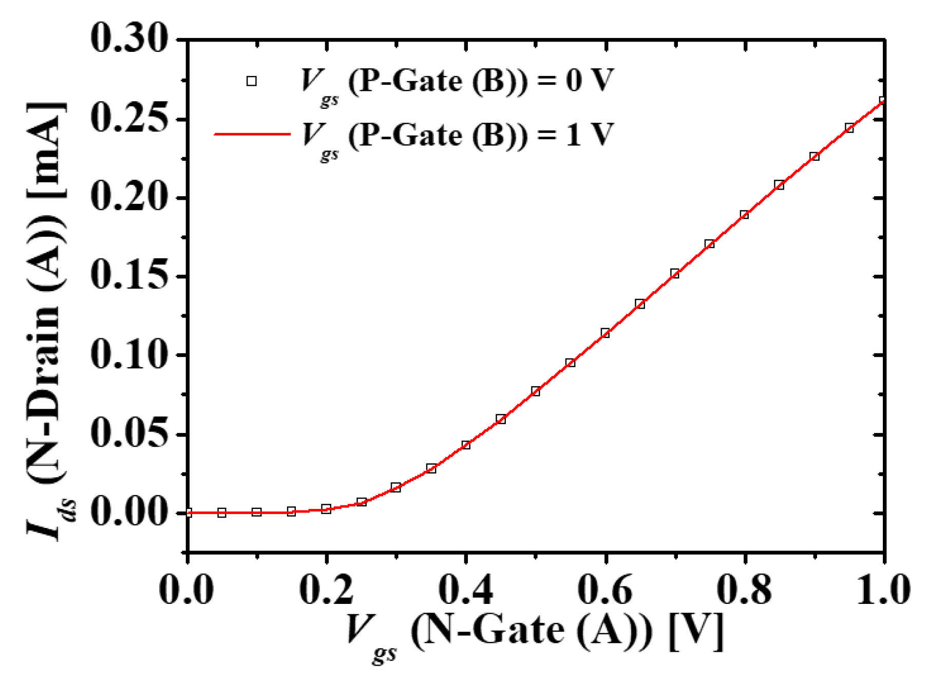
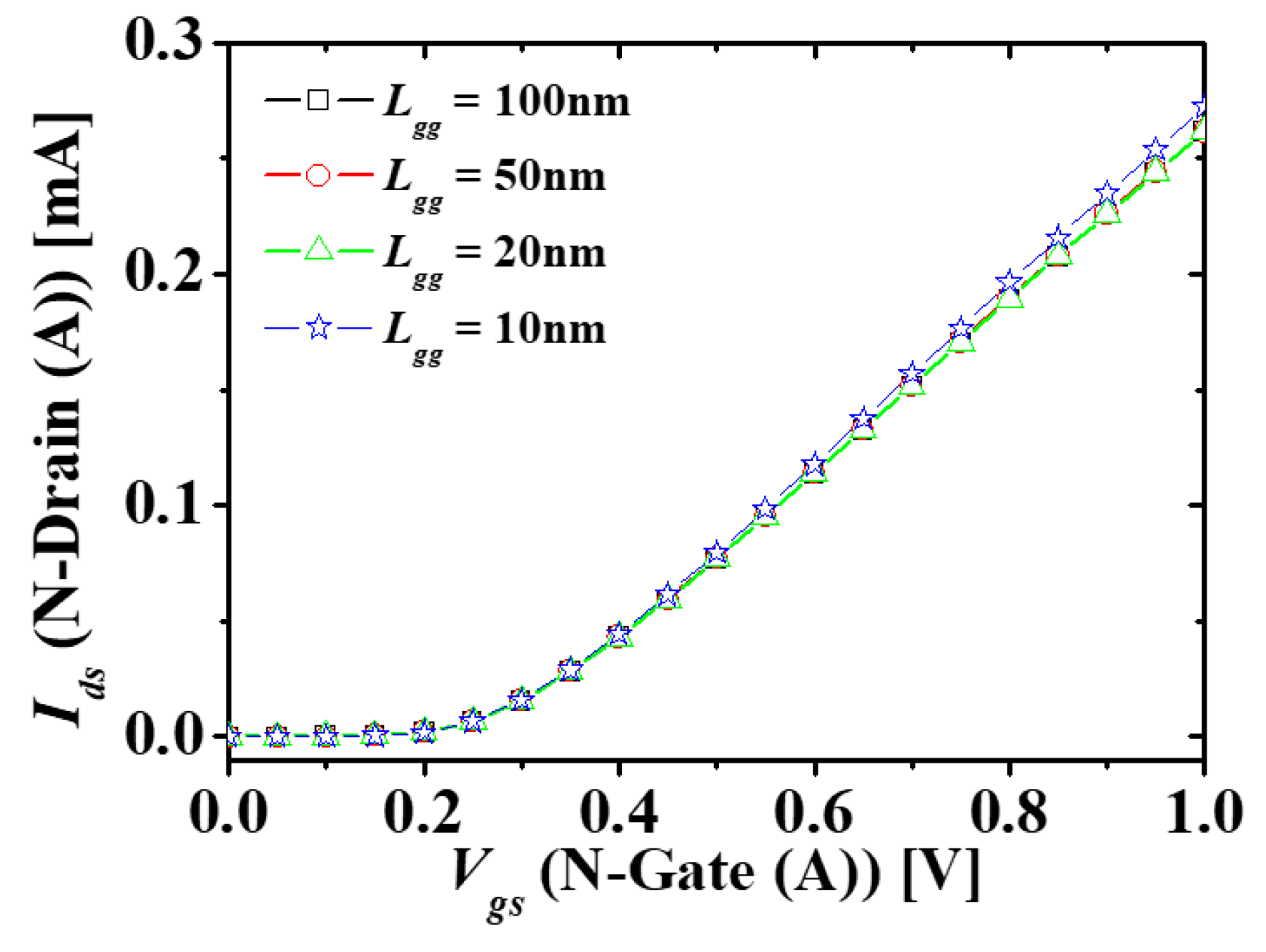
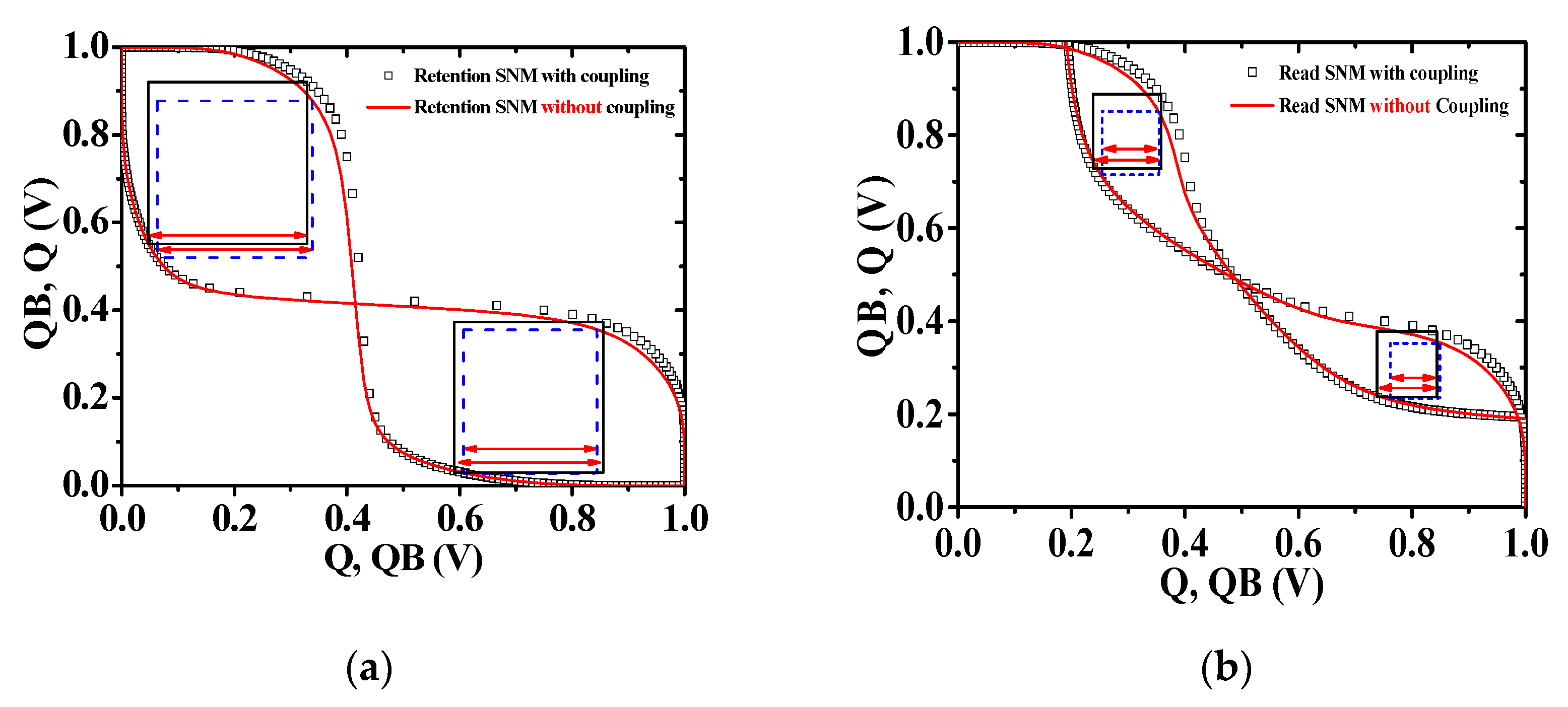
4. Simulation and Discussion
5. Conclusions
Author Contributions
Funding
Acknowledgments
Conflicts of Interest
References
- Claverlier, L.; Deguet, C.; di Cioccio, L.; Augendre, E.; Brugere, A.; Gueguen, P.; Tiec, Y.L.; Moriceau, H.; Rabarot, M.; Signamarcheix, T.; et al. Engineered substrates for future More Moore and More than Moore integrated devices. In Proceedings of the 2010 IEEE International Electron Devices Meeting (IEDM), San Francisco, CA, USA, 6–8 December 2010; pp. 261–264. [Google Scholar] [CrossRef]
- Park, K.T.; Nam, S.W.; Kim, D.H.; Kwak, P.S.; Lee, D.S.; Choi, Y.H.; Choi, M.H.; Kwak, D.H.; Kim, D.H.; Kim, M.S.; et al. Three-dimensional 128 Gb MLC vertical nand flash memory with 24-WL stacked layers and 50 MB/s high-speed programming. IEEE J. Solid State Circuits 2015, 50, 204–213. [Google Scholar] [CrossRef]
- Lee, S.Y.; Park, J.I. Architecture of 3D memory cell array on 3D IC. In Proceedings of the 2012 4th IEEE International Memory Workshop, Milan, Italy, 20–23 May 2012; pp. 1–3. [Google Scholar] [CrossRef]
- Shen, C.-H.; Shieh, J.-M.; Wu, T.-T.; Huang, W.-H.; Yang, C.-C.; Wan, C.-J.; Lin, C.-D.; Wang, H.-H.; Chen, B.-Y.; Huang, G.-W.; et al. Monolithic 3D chip integrated with 500ns NVM, 3ps logic circuits and SRAM. In Proceedings of the 2013 IEEE International Electron Devices Meeting, Washington, DC, USA, 9–11 December 2013; pp. 931–934. [Google Scholar] [CrossRef]
- Shulaker, M.M.; Wu, T.F.; Pal, A.; Zhao, L.; Nishi, Y.; Saraswat, K.; Wong, H.-S.P.; Mitra, S. Monolithic 3D integration of logic and memory: Carbon nanotube FETs, resistive RAM, and silicon FETs. In Proceedings of the 2014 IEEE International Electron Devices Meeting, San Francisco, CA, USA, 15–17 December 2014; pp. 2741–2744. [Google Scholar] [CrossRef]
- Li, S.K. Bringing 3D ICs to aerospace: Needs for design tools and methodologies. J. Inf. Commun. Converg. Eng. 2017, 15, 117–122. [Google Scholar] [CrossRef]
- Schuegraf, K.; Abraham, M.C.; Naik, M.; Thakur, R. Semiconductor logic technology innovation to achieve sub-10 nm manufacturing. IEEE J. Electron Devices Soc. 2013, 3, 66–75. [Google Scholar] [CrossRef]
- Santos, C.; Vivet, P.; Thuries, S.; Billoint, O.; Colonna, J.-P.; Coudrain, P.; Wang, L. Thermal performance of CoolCube™ monolithic and TSV-based 3D integration processes. In Proceedings of the IEEE International 3D Systems Integration Conference (3DIC), San Francisco, CA, USA, 8–11 November 2016; pp. 1–5. [Google Scholar] [CrossRef]
- Llorente, C.D.; Royer, C.L.; Batude, P.; Fenouillet-Beranger, C.; Martinie, S.; Lu, C.-M.V.; Allain, F.; Colinge, J.-P.; Cristoloveanu, S.; Ghibaudo, G.; et al. New insights on SOI tunnel FETs with low-temperature process flow for CoolCubeTM integration. Solid State Electron. 2018, 144, 78–85. [Google Scholar] [CrossRef]
- Batude, P.; Ernst, T.; Arcamone, J.; Arndt, G.; Coudrain, P.; Gaillardon, P.-E. 3-D sequential integration: A key enabling technology for heterogeneous co-integration of new function with CMOS. IEEE J. Emerg. Sel. Top. Circuits Syst. 2012, 2, 714–722. [Google Scholar] [CrossRef]
- Vinet, M.; Batude, P.; Fenouillet-Beranger, C.; Clermidy, F.; Brunet, L.; Rozeau, O.; Hartmannn, J.M.; Billoint, O.; Cibrario, G.; Previtali, B.; et al. Monolithic 3D integration: A powerful alternative to classical 2D scaling. In Proceedings of the 2014 SOI-3D-Subthreshold Microelectronics Technology Unified Conference (S3S), Millbrae, CA, USA, 6–9 October 2014; pp. 1–3. [Google Scholar] [CrossRef]
- Sachid, A.B.; Tosun, M.; Desai, S.B.; Hsu, C.-Y.; Lien, D.-H.; Madhvapathy, S.R.; Chen, Y.-Z.; Hettick, M.; Kang, J.S.; Zeng, Y.; et al. Monolithic 3D CMOS using layered semiconductors. Adv. Mater. 2016, 28, 2547–2554. [Google Scholar] [CrossRef] [PubMed]
- Yu, Y.S.; Panth, S.; Lim, S.K. Electrical coupling of monolithic 3-D inverters. IEEE Trans. Electron Devices 2016, 63, 3346–3349. [Google Scholar] [CrossRef]
- Ahn, T.J.; Perumal, R.; Lim, S.K.; Yu, Y.S. Parameter extraction and power/performance analysis of monolithic 3-D inverter (M3INV). IEEE Trans. Electron Devices 2019, 66, 1006–1011. [Google Scholar] [CrossRef]
- Silvaco Int. ATLAS ver. 5. 20. 2. R Manual; Silvaco Int.: Santa Clara, CA, USA, 2015. [Google Scholar]
- IC STMicroelectronics 28nm Advanced CMOS FDSOI 8 ML. Available online: https://mycmp.fr/datasheet/ic-28nm-cmos28fdsoi. (accessed on 20 June 2019).
- Rozeau, O.; Jaud, M.-A.; Poiroux, T.; Benosman, M. UTSOI Model 1.1.3. Laboratoire d’Électronique et de Technologie de l’Information (Leti). Available online: http://www-leti.cea.fr (accessed on 25 May 2012).
- Rani, T.E.; Rani, M.A.; Rao, R. AREA optimized low power arithmetic and logic unit. In Proceedings of the International Conference on Electronics Computer Technology, Kanyakumari, India, 8–10 April 2011; pp. 224–228. [Google Scholar] [CrossRef]
- Nasrollahpour, M.; Sreekumar, R.; Hajilou, F.; Aldacher, M.; Hamedi-Hagh, S. Low-power bluetooth receiver front end design with oscillator leakage reduction technique. J. Low Power Electron. 2018, 14, 1–6. [Google Scholar] [CrossRef]
- Lee, Y.J.; Limbrick, D.; Lim, S.K. Power benefit study for ultra-high density transistor-level monolithic 3D ICs. In Proceedings of the 50th Annual Design Automation Conference, Austin, TX, USA, 29 May–7 June 2013; pp. 1–19. [Google Scholar] [CrossRef]
- Arandilla, C.D.C.; Alvarez, A.B.; Roque, C.R.K. Static noise margin of 6T SRAM cell in 90-nm CMOS. In Proceedings of the UkSim 13th International Conference on Computer Modelling and Simulation, Cambridge, UK, 30 March–1 April 2011; pp. 534–539. [Google Scholar] [CrossRef]

| Models/Parameters | Description | Value/Unit |
|---|---|---|
| CVT | Lombardi model and complete mobility model including doping density N, temperature T, and transverse electric field E//. | – |
| SRH | Shockley–Read–Hall recombination model | – |
| AUGER | Auger recombination model | – |
| FERMI | Fermi–Dirac carrier statistics | – |
| NEWTON | Newton method which solves a linearlized version of the entire nonlinear algebraic system | – |
| GUMMEL | Gummel method which solves a sequence of relatively small linear subproblems | – |
| ΦN | Gate work function of NMOSFET | 4.57 eV |
| ΦP | Gate work function of PMOSFET | 4.9 eV |
| Symbols | Description | Value (fF) |
|---|---|---|
| Cngns/Cngps | Top gate-top/bottom source capacitances of MOSFETs | 0.0316/0.0006 |
| Cpgns/Cpgps | Bottom gate-top/bottom source capacitances of MOSFETs | 0.0007/0.08 |
| Cngnd/Cngpd | Top gate-top/bottom drain capacitances of MOSFETs | 0.0325/0.0018 |
| Cpgnd/Cpgpd | Bottom gate-top/bottom drain capacitances of top/bottom MOSFETs | 0.0007/0.08 |
| Cndns/Cndps | Top drain-top/bottom source capacitances of MOSFETs | n.s./0.0001 |
| Cpdns/Cpdps | Bottom drain-top/bottom source capacitances of MOSFETs | 0.0002/n.s. |
| Cngsub/Cpgsub | Gate-substrate capacitances of top/bottom MOSFETs | n.s./n.s. |
| Csubnd/Csubpd | Substrate-top/bottom drain capacitances of MOSFETs | n.s./0.0011 |
| Performances | M3D with TILD = 100 nm (Neglecting VCE) | M3D with TILD = 10 nm (Including VCE) | ||||||||
|---|---|---|---|---|---|---|---|---|---|---|
| INV | NAND | NOR | MUX | D-FF | INV | NAND | NOR | MUX | D-FF | |
| Static power (nW) | 5.1 | 3.97 | 5.17 | 7.1 | 42.2 | 4.89 | 1.63 | 2.41 | 4.21 | 17.4 |
| (−4.1%) | (−58%) | (−53.3%) | (−40.7%) | (−58.7%) | ||||||
| Dynamic power (μW) | 8.55 | 12.4 | 12.2 | 18.4 | 39.3 | 9.85 | 13.9 | 13.8 | 22.6 | 41.9 |
| (15.2%) | (12%) | (13.1%) | (22.8%) | (6.6%) | ||||||
| Cell area (μm2) | 0.043 | 0.087 | 0.087 | 0.013 | 0.261 | 0.043 | 0.087 | 0.087 | 0.13 | 0.261 |
| (0.101 *) | (0.217 *) | (0.217 *) | (0.986 *) | (2.117 *) | (−57.4%) | (−59.9%) | (−59.9%) | (−86%) | (−87%) | |
| Average delay (ps) | 3.875 | 4.925 | 4.64 | 1.95 | 8.35 | 4.93 | 5.45 | 5.22 | 2.3 | 10.25 |
| (27.2%) | (10.6%) | (12.5%) | (17.9%) | (22.7%) | ||||||
© 2019 by the authors. Licensee MDPI, Basel, Switzerland. This article is an open access article distributed under the terms and conditions of the Creative Commons Attribution (CC BY) license (http://creativecommons.org/licenses/by/4.0/).
Share and Cite
Ahn, T.J.; Choi, B.H.; Lim, S.K.; Yu, Y.S. Electrical Coupling and Simulation of Monolithic 3D Logic Circuits and Static Random Access Memory. Micromachines 2019, 10, 637. https://doi.org/10.3390/mi10100637
Ahn TJ, Choi BH, Lim SK, Yu YS. Electrical Coupling and Simulation of Monolithic 3D Logic Circuits and Static Random Access Memory. Micromachines. 2019; 10(10):637. https://doi.org/10.3390/mi10100637
Chicago/Turabian StyleAhn, Tae Jun, Bum Ho Choi, Sung Kyu Lim, and Yun Seop Yu. 2019. "Electrical Coupling and Simulation of Monolithic 3D Logic Circuits and Static Random Access Memory" Micromachines 10, no. 10: 637. https://doi.org/10.3390/mi10100637
APA StyleAhn, T. J., Choi, B. H., Lim, S. K., & Yu, Y. S. (2019). Electrical Coupling and Simulation of Monolithic 3D Logic Circuits and Static Random Access Memory. Micromachines, 10(10), 637. https://doi.org/10.3390/mi10100637