Author Contributions
Conceptualization, Y.C. and X.Z.; methodology, Y.C. and X.Z.; software, Y.C.; validation, Y.C., X.Z., X.L., and Y.M.; formal analysis, Y.C. and X.Z.; investigation, X.Z.; resources, Y.C.; data curation, Y.C.; writing—original draft preparation, X.L.; writing—review and editing, X.L.; project administration, X.Z. and Y.M.; funding acquisition, X.Z. and Y.M. All authors have read and agreed to the published version of the manuscript.
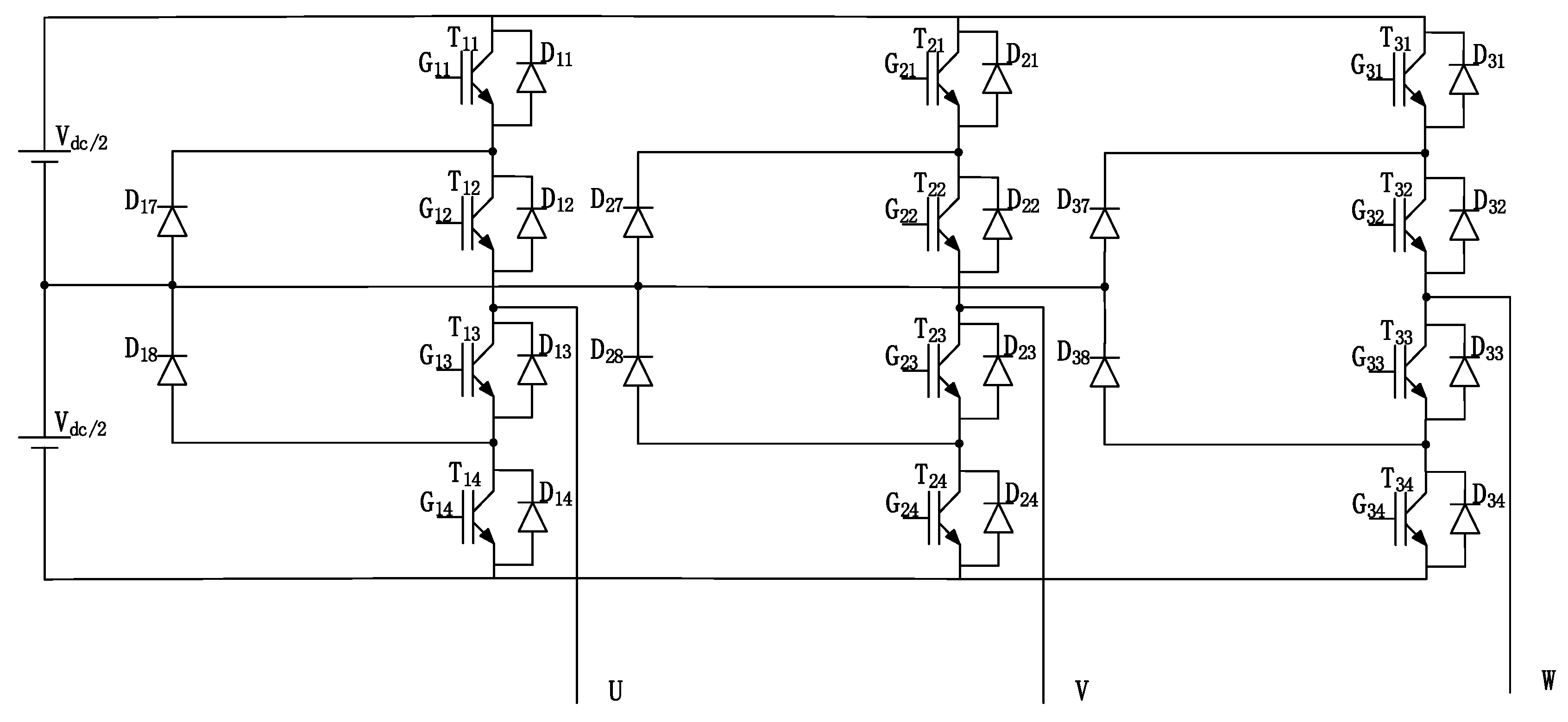
Figure 1.
Traditional D-NPC (diode neutral-point-clamped) topology.
Figure 1.
Traditional D-NPC (diode neutral-point-clamped) topology.
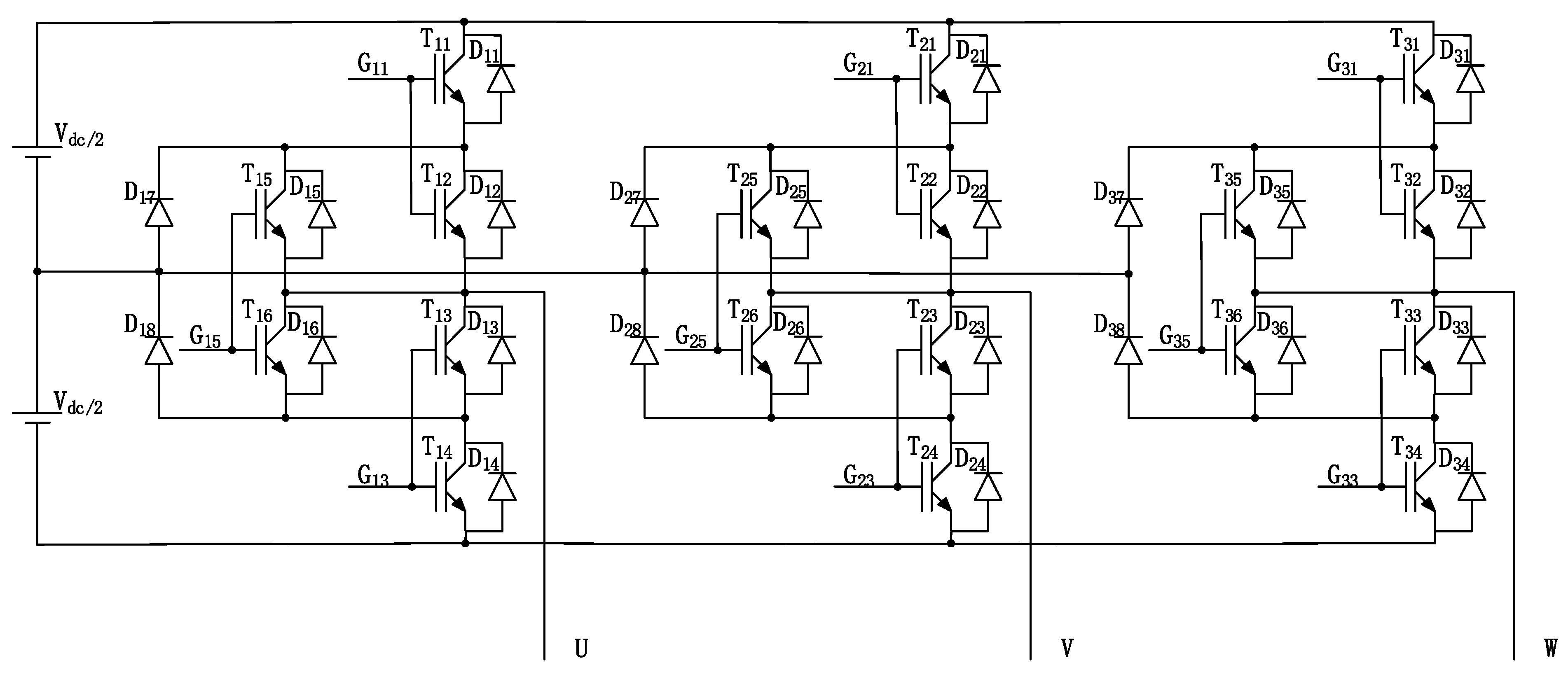
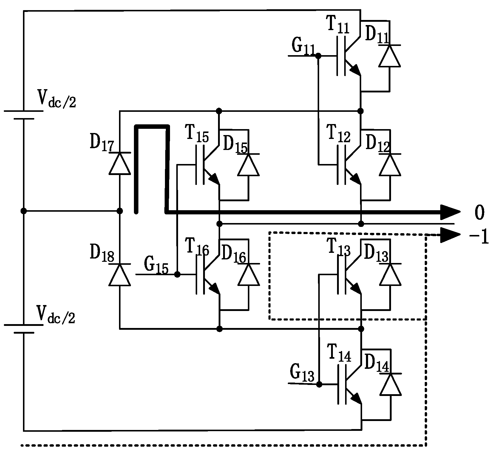
Figure 2.
The ID-NPC (improved diode neutral-point-clamped) topology.
Figure 2.
The ID-NPC (improved diode neutral-point-clamped) topology.
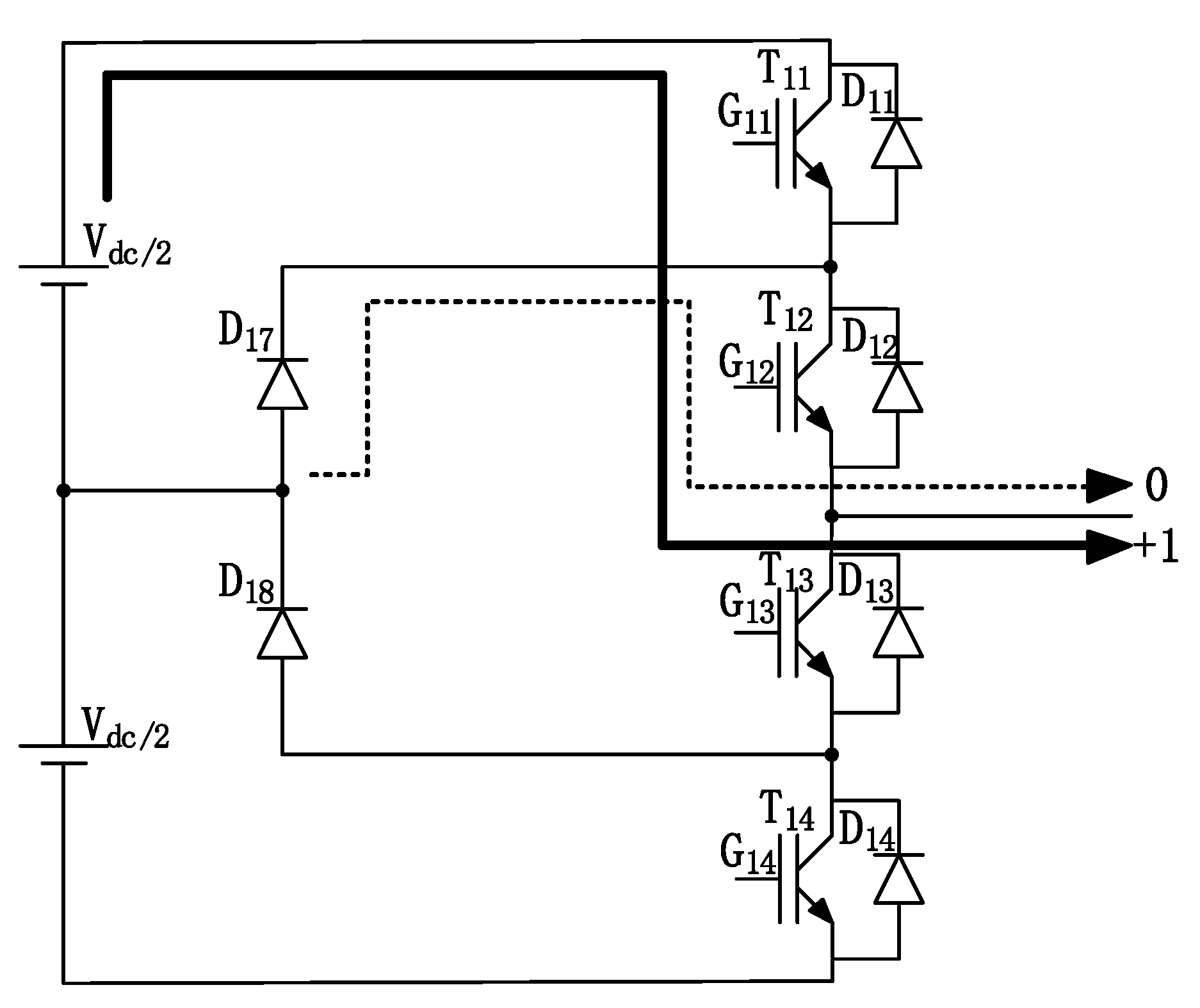
Figure 3.
D1 type (α = +1, M ≈ 0).
Figure 3.
D1 type (α = +1, M ≈ 0).
Figure 4.
D2 type (α = −1, M = 1.15).
Figure 4.
D2 type (α = −1, M = 1.15).
Figure 5.
D3 type (α = +1, M ≈ 0).
Figure 5.
D3 type (α = +1, M ≈ 0).
Figure 6.
D4 type (α = −1, M ≈ 0).
Figure 6.
D4 type (α = −1, M ≈ 0).
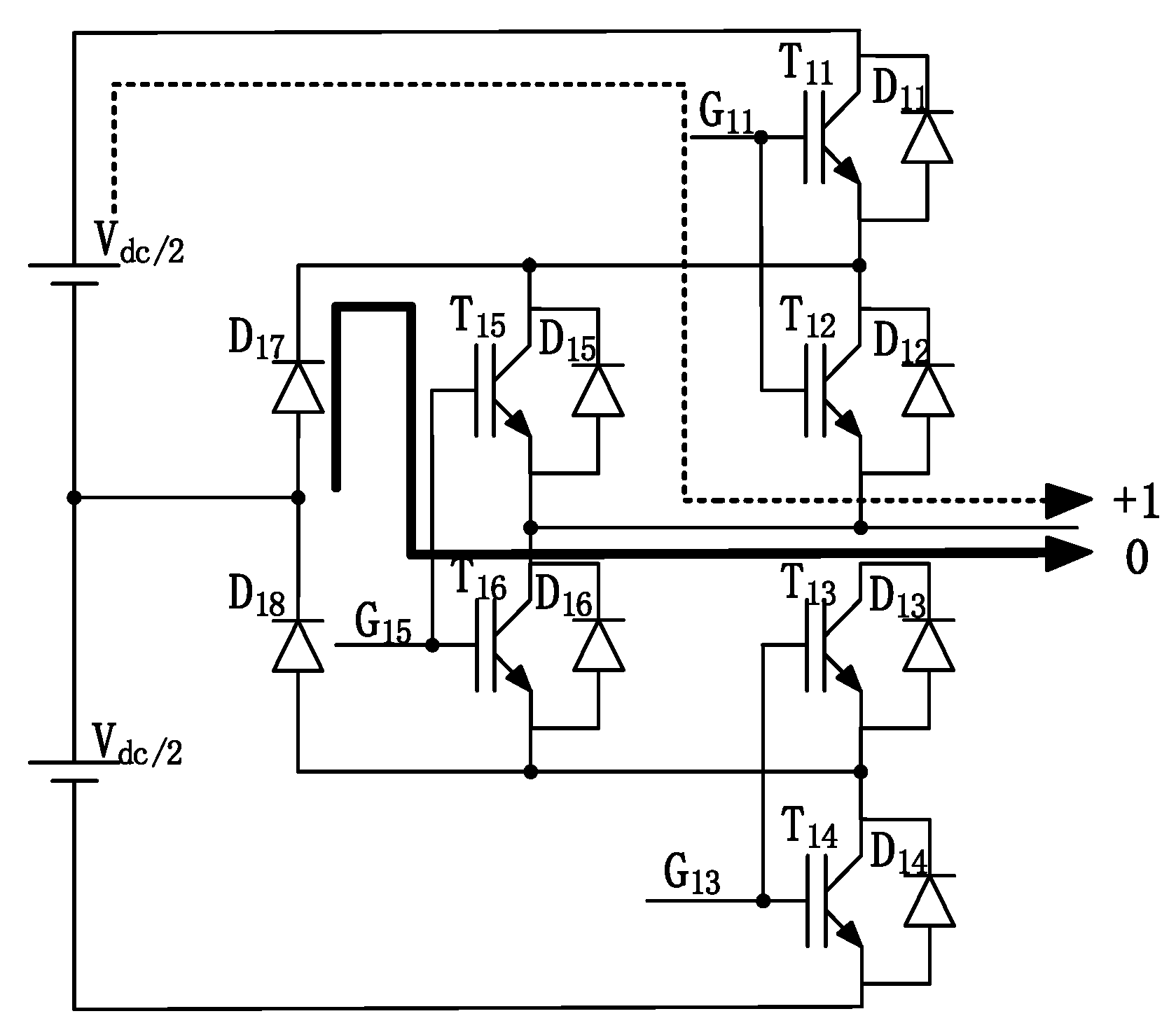
Figure 7.
ID1 type (α = +1, M = 1.15).
Figure 7.
ID1 type (α = +1, M = 1.15).
Figure 8.
ID2 type (α = −1, M = 1.15).
Figure 8.
ID2 type (α = −1, M = 1.15).
Figure 9.
ID3 type (α = +1, M ≈ 0).
Figure 9.
ID3 type (α = +1, M ≈ 0).
Figure 10.
ID4 type (α = −1, M ≈ 0).
Figure 10.
ID4 type (α = −1, M ≈ 0).
Figure 11.
Improved two-level topology.
Figure 11.
Improved two-level topology.
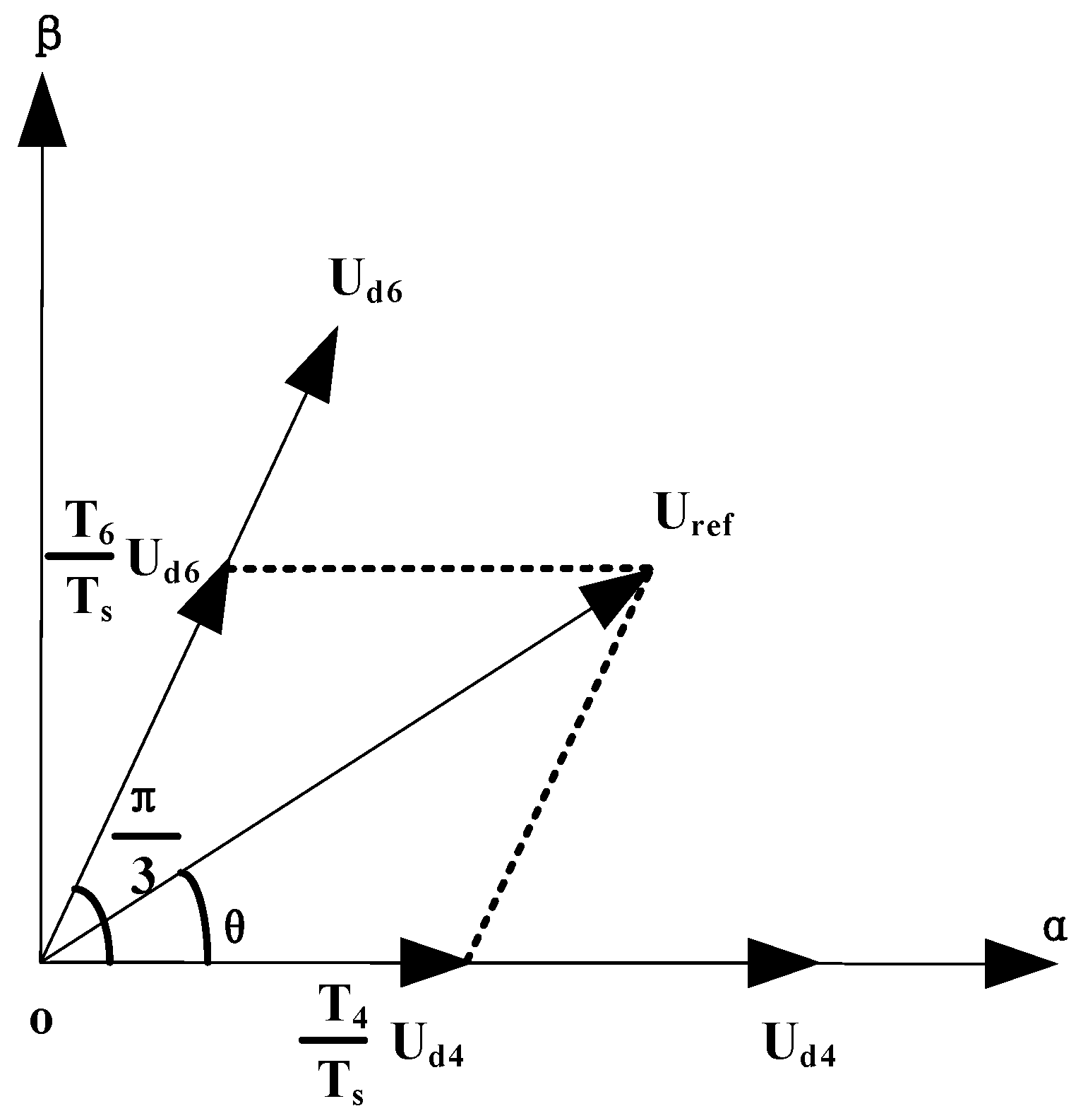
Figure 12.
The vector composition in the ) region.
Figure 12.
The vector composition in the ) region.
Figure 13.
The flowchart of modulation conversion.
Figure 13.
The flowchart of modulation conversion.
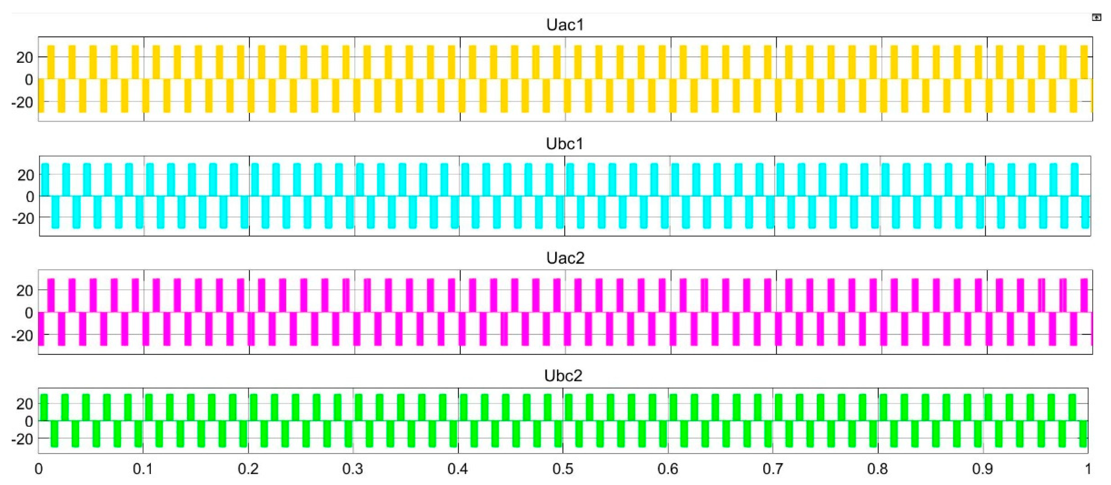
Figure 14.
The simulation waveforms based on two topologies.
Figure 14.
The simulation waveforms based on two topologies.
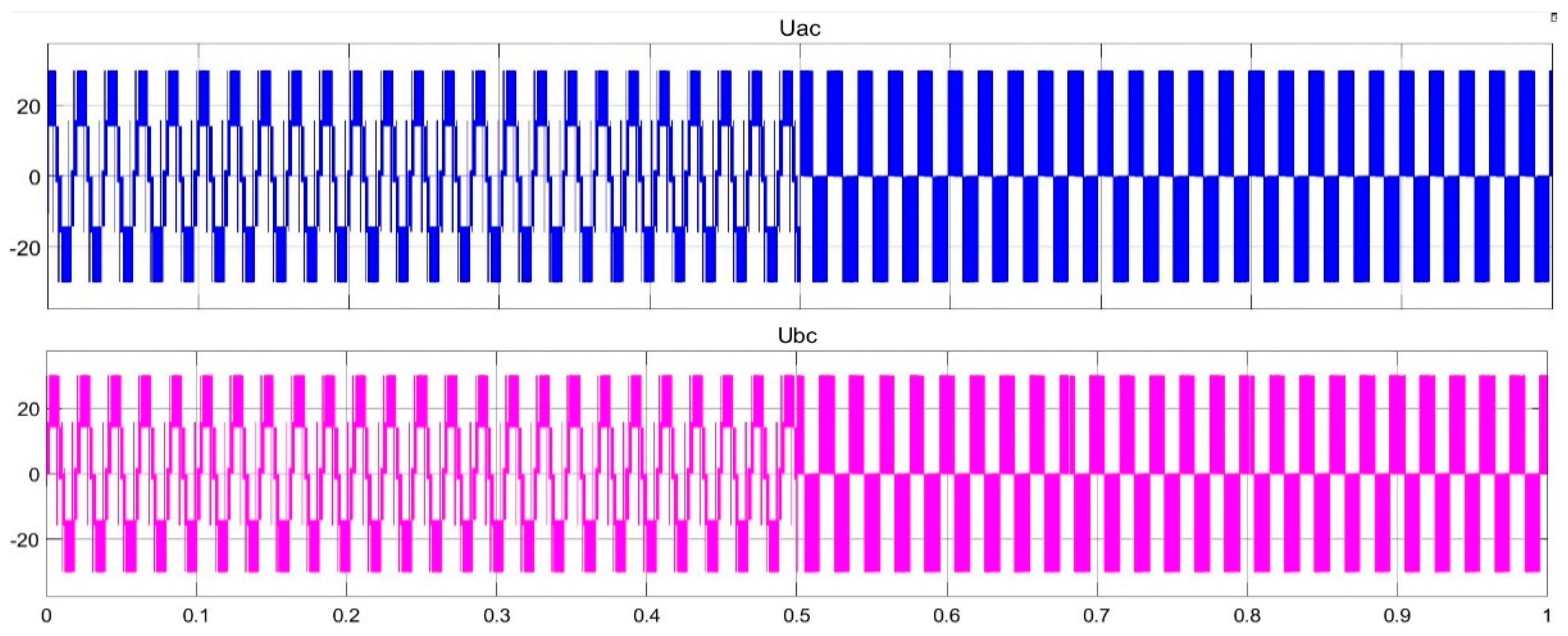
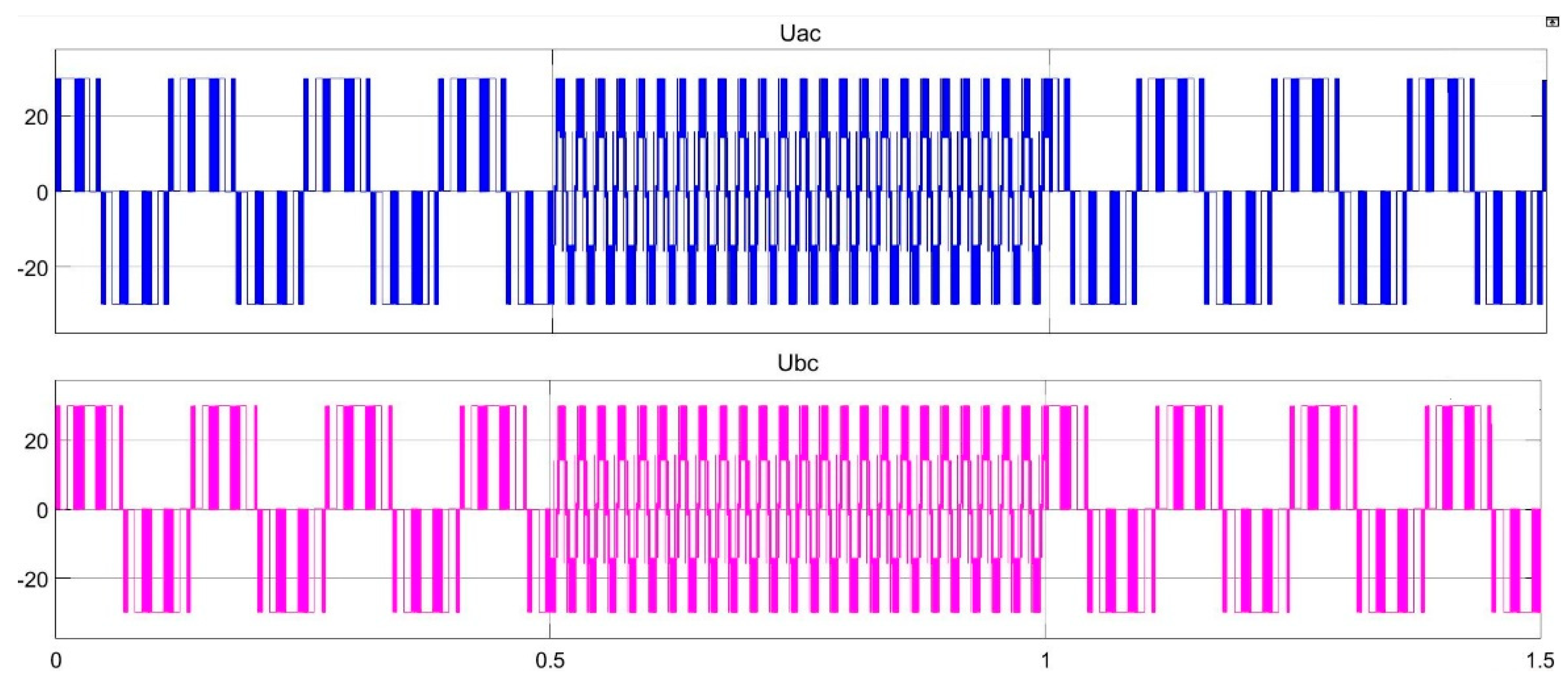
Figure 15.
The simulation voltage waveform of three–two-level modulation conversion.
Figure 15.
The simulation voltage waveform of three–two-level modulation conversion.
Figure 16.
The simulation voltage waveform of two–three-level modulation conversion.
Figure 16.
The simulation voltage waveform of two–three-level modulation conversion.
Figure 17.
The simulation voltage waveform of the whole conversion process.
Figure 17.
The simulation voltage waveform of the whole conversion process.
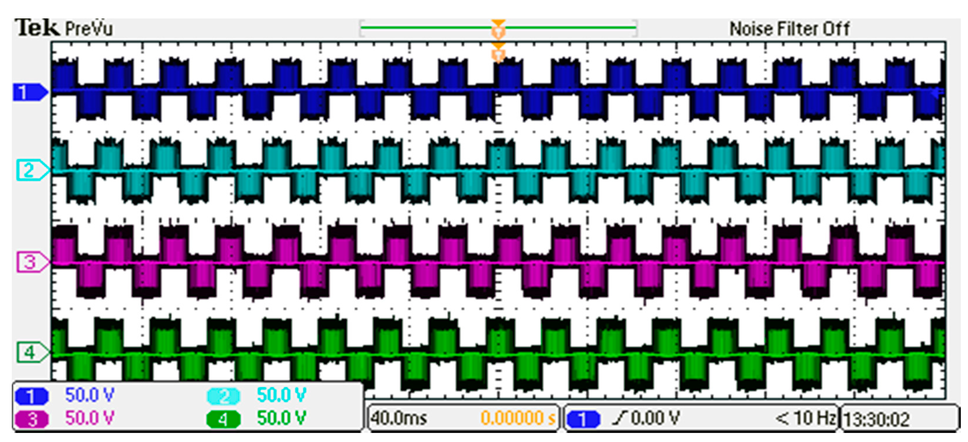
Figure 18.
The experimental waveforms of two topologies.
Figure 18.
The experimental waveforms of two topologies.
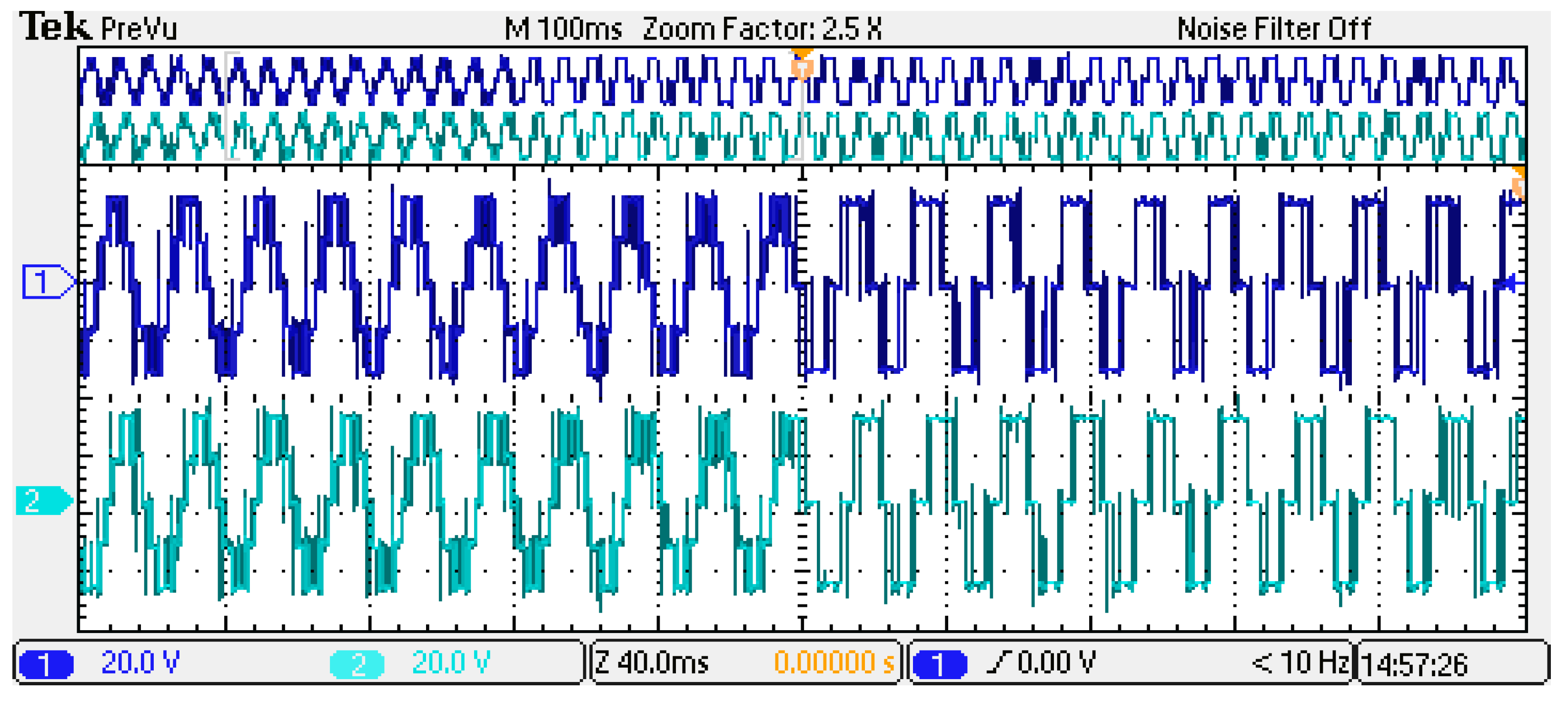
Figure 19.
The experimental waveform of three–two-level modulation conversion.
Figure 19.
The experimental waveform of three–two-level modulation conversion.
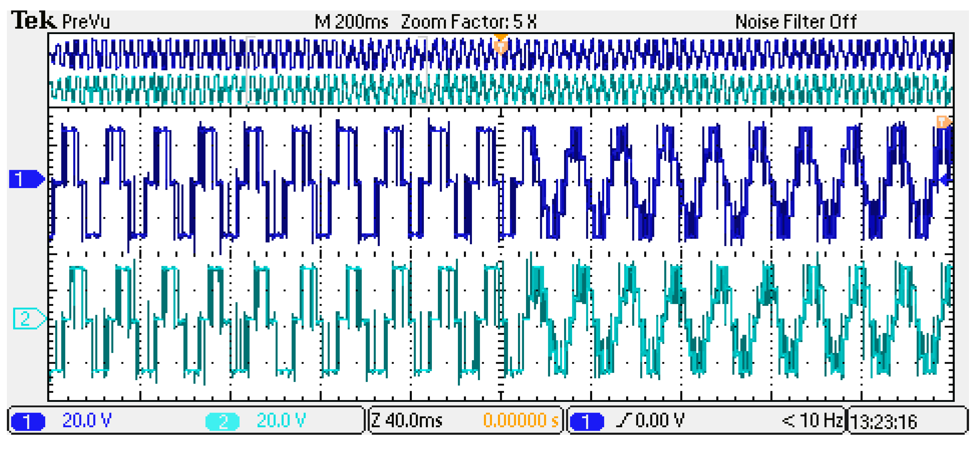
Figure 20.
The experimental waveform of two–three-level modulation conversion.
Figure 20.
The experimental waveform of two–three-level modulation conversion.
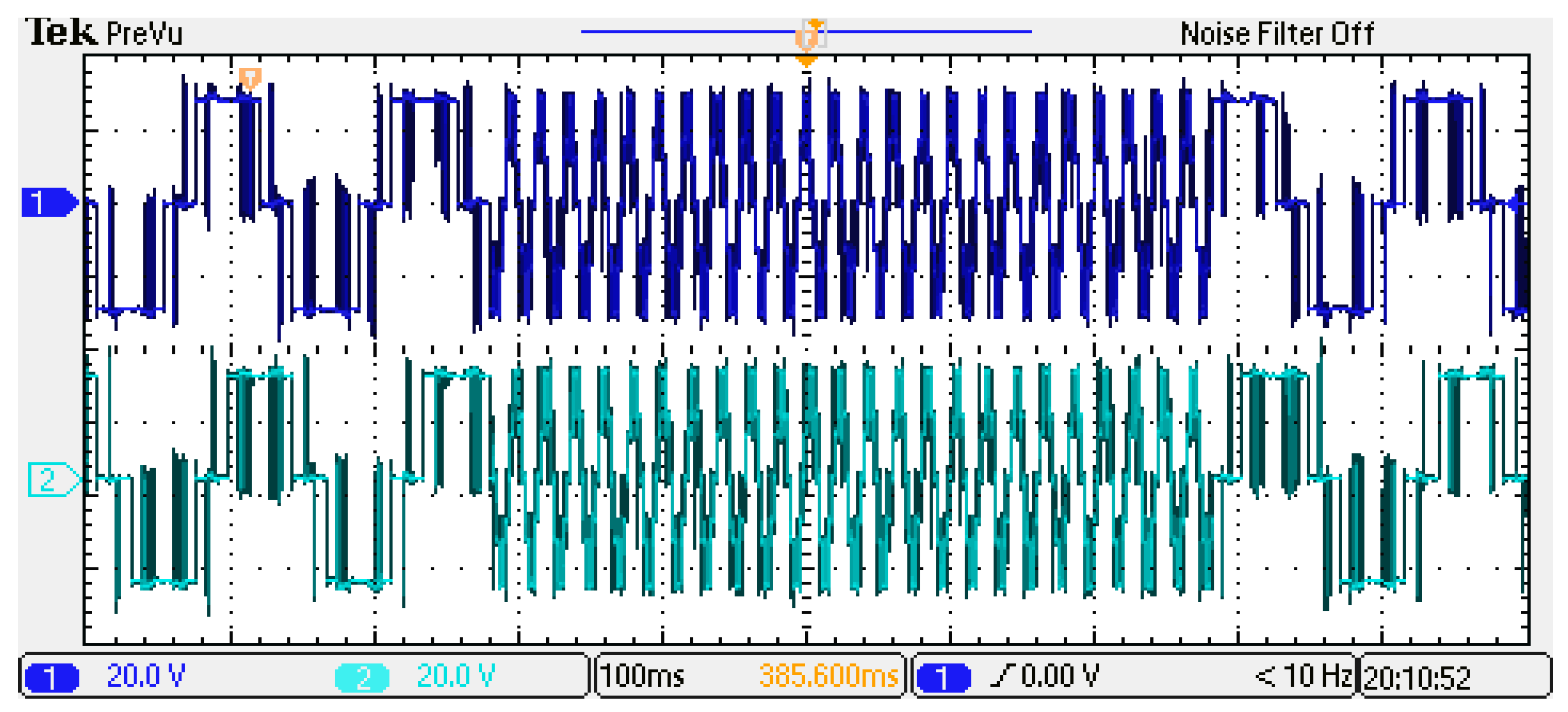
Figure 21.
The whole conversion process of the modulation strategy.
Figure 21.
The whole conversion process of the modulation strategy.
Table 1.
The comparison of four traditional topologies.
Table 1.
The comparison of four traditional topologies.
| Topological Structure | Two-Level | D-NPC | A-NPC | T-NPC |
|---|
| Number of IGBT | 2 | 4 | 6 | 4 |
| Number of driving paths | 2 | 4 | 6 | 4 |
| Number of diodes | 2 | 6 | 6 | 4 |
| Device withstand voltage | Vdc | Vdc/2 | Vdc/2 | Horizontal switch: Vdc/2
Vertical switch: Vdc |
| Control difficulty | Easy | More difficult | Most difficult | More difficult |
| Withstand voltage | No | Capacitance | Capacitance | Capacitance |
| Output level | 2 | 3 | 3 | 3 |
| Conduction loss | Minimum | Large | Large | Maximum |
| Switching loss | Large | Low | Low | Maximum |
| Heat distribution | Balance | Imbalance | Algorithmic balance | Balance |
Table 2.
D-NPC (diode neutral-point-clamped) switching table.
Table 2.
D-NPC (diode neutral-point-clamped) switching table.
| Switching | G11 | G12 | G13 | G14 |
|---|
| “+” | 1 | 1 | 0 | 0 |
| “0” | 0 | 1 | 1 | 0 |
| “−” | 0 | 0 | 1 | 1 |
Table 3.
ID-NPC switching table.
Table 3.
ID-NPC switching table.
| Switching | G11 | G15 | G13 |
|---|
| “+” | 1 | 0 | 0 |
| “0” | 0 | 1 | 0 |
| “−” | 0 | 0 | 1 |
Table 4.
D-NPC switching loss table.
Table 4.
D-NPC switching loss table.
| α | M | T | State | T11 | D11 | T12 | D12 | T13 | D13 | T14 | D14 | T15 | D15 | T16 | D16 | D17 | D18 |
|---|
| +1 | 1.15 | D1 | “+”⟷“0” | √ | | | | ○ | | | | | | | | ○ | |
| −1 | 0 | D2 | “0”⟷“−” | | | √ | | ○ | ○ | ○ | ○ | | | | | √ | |
| +1 | 1.15 | D3 | “+”⟷“0” | √ | | | | ○ | | | | | | | | ○ | |
| −1 | 0 | D4 | “0”⟷“−” | | | √ | | ○ | ○ | ○ | ○ | | | | | √ | |
Table 5.
ID-NPC switching loss table.
Table 5.
ID-NPC switching loss table.
| α | M | T | State | T11 | D11 | T12 | D12 | T13 | D13 | T14 | D14 | T15 | D15 | T16 | D16 | D17 | D18 |
|---|
| +1 | 1.15 | D1 | “+”⟷“0” | √ | | √ | | | | | | ○ | | ○ | | ○ | |
| −1 | 0 | D2 | “0”⟷“−” | | | | | ○ | ○ | ○ | ○ | √ | | √ | ○ | √ | |
| +1 | 1.15 | D3 | “+”⟷“0” | √ | | √ | | | | | | ○ | | ○ | | ○ | |
| −1 | 0 | D4 | “0”⟷“−” | | | | | ○ | ○ | ○ | ○ | √ | | √ | ○ | √ | |
Table 6.
Corresponding relationship of sector, basic vector, αβ coordinate system region order, and RAM.
Table 6.
Corresponding relationship of sector, basic vector, αβ coordinate system region order, and RAM.
| Sector | Basic Vector | | RAM |
|---|
| III | T4, T6 | | 1–683 |
| I | T6, T2 | | 684–1366 |
| V | T2, T3 | | 1367–2048 |
| IV | T3, T1 | | 2049–2731 |
| VI | T1, T5 | | 2732–3414 |
| II | T5, T4 | | 3415–4096 |
Table 7.
Relationship between the sector action time and the sector.
Table 7.
Relationship between the sector action time and the sector.
| Order | Ti | Tj | T0 |
|---|
| ()(T4, T6) | | | |
| ()(T6, T2) | | | |
| (T2, T3) | | | |
| (T3, T1) | | | |
| (T1, T5) | | | |
| (T5, T4) | | | |
Table 8.
The relationship between angle and action time.
Table 8.
The relationship between angle and action time.
| Order | Ti | Tj | T0 |
|---|
| RAM value | 1–683 | 1–683 | 1–683 |
| ()(T4, T6) | | | |
| RAM value | 684–1366 | 684–1366 | 684–1366 |
| ()(T6, T2) | | | |
| RAM value | 1367–2048 | 1367–2048 | 1367–2048 |
| ()(T2, T3) | | | |
| RAM value | 2049–2731 | 2049–2731 | 2049–2731 |
| ()(T3, T1) | | | |
| RAM value | 2732–3414 | 2732–3414 | 2732–3414 |
| ()(T1, T5) | | | |
| RAM value | 3415–4096 | 3415–4096 | 3415–4096 |
| ((T5, T4) | | | |
Table 9.
Simulation conditions.
Table 9.
Simulation conditions.
| Name | DC Voltage | | | |
|---|
| Value | 30 V | 10 | | |


