3.1. Microstructure Evolution During the Rolling Process
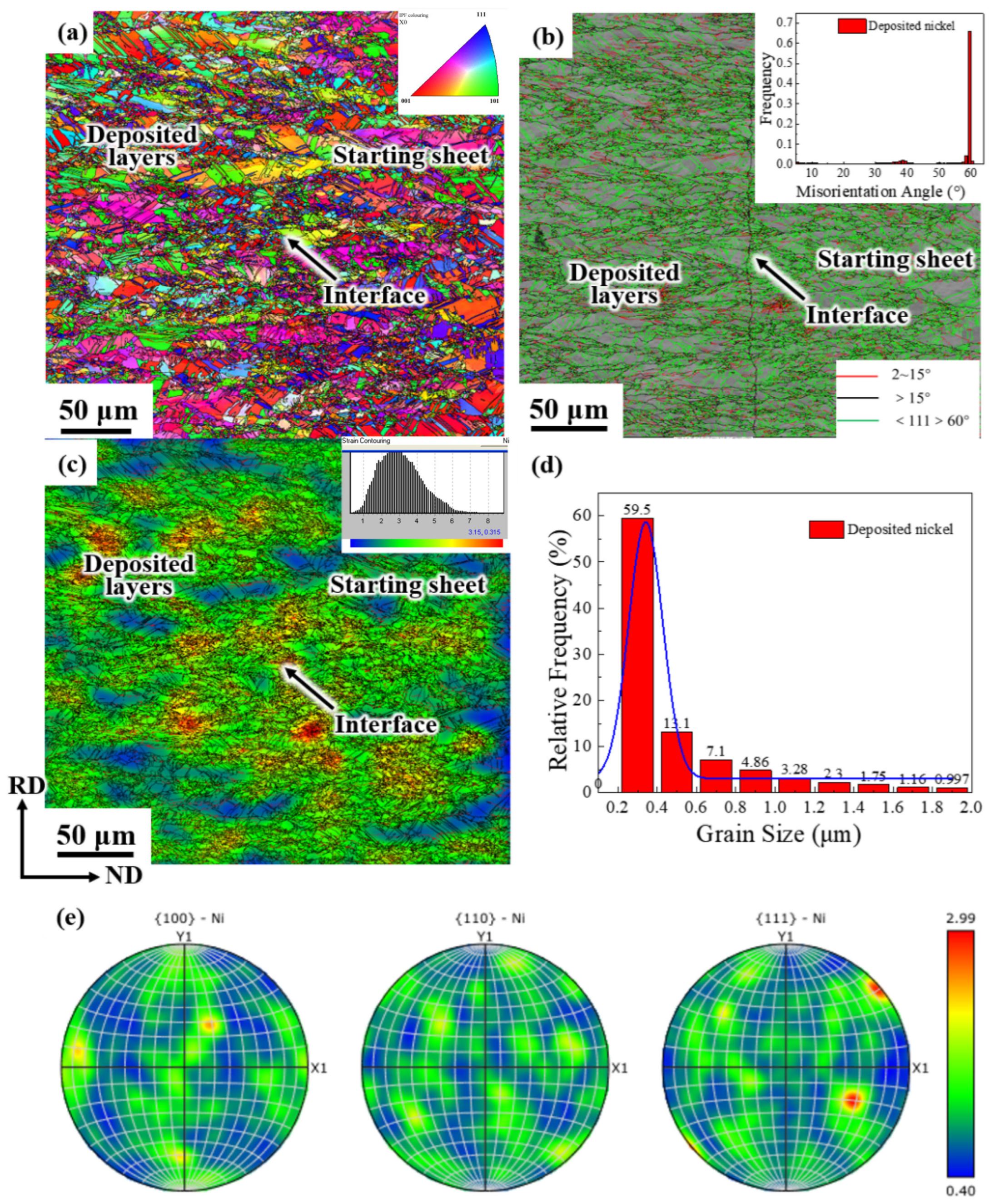
Figure 2 presents the EBSD diagram of deposited electrolytic nickel, where the ND direction represents the deposition direction. From the grain orientation distribution shown in
Figure 2a, it is evident that the grain size of the deposited electrolytic nickel is uneven, with a large number of equiaxed and columnar crystals of varying sizes. In
Figure 2b, the green line represents the <111> 60° twin boundary. A large number of growth twins with varying lengths and thicknesses, accounting for over 70%, are present in the deposited electrolytic nickel. These twinning structures correspond to the lamellar structures observed in
Figure 1, which either extend through the entire grain or cease growing within the grain. Pure nickel is a metal with medium to high dislocation energy, and the occurrence of numerous growth twins in electrolytic nickel has rarely been reported in the literature. Materials with high-density growth twins are generally found in electrolytic copper or other electrolytic alloys with lower dislocation energy.
Figure 2c shows the strain cloud diagram of the microstructure (strain contouring), which highlights the uneven stress distribution within the electrolytic nickel microstructure. Internal stress is generated and retained during the electrodeposition process [
28]. From the grain size distribution of electrolytic nickel shown in
Figure 2d, it can be observed that grains with a size of 0.3 μm account for approximately 59.5%, grains smaller than 0.5 μm make up about 72.6%, and grains smaller than 1.0 μm account for 84.56%. The average grain size of electrolytic nickel is 0.56 μm.
Figure 2d shows that although the grain size distribution range of electrolytic nickel is wide, with large grains reaching over 20 μm, the overall grain size is relatively fine, with most of the grains at the nanometer level. The deposited layer near the starting sheet consists of very fine equiaxed grains, while the deposited layer farther from the starting sheet gradually exhibits columnar growth and larger grains. This phenomenon occurs because, when nickel ions first deposit on the surface of the starter electrode sheet, their nucleation rate is much higher than the crystal growth rate, resulting in the formation of a layer of fine equiaxed grains adhering to the surface. At this stage, the growth mode of electrolytic nickel grains follows a “nucleation growth mode”. During the nickel deposition process, a large number of crystal nuclei form on the cathode (the starting sheet) surface. As these crystal nuclei grow and meet, their growth halts, forming fine equiaxed crystal regions. Subsequently, when the growth rate of the crystal nuclei surpasses the nucleation rate, the crystals begin to extend along the growth direction, forming columnar crystals and transitioning into a rapid growth mode. Columnar crystals whose growth direction is parallel to the normal of the matrix are able to grow further due to sufficient space. However, the growth directions of these columnar crystals and secondary dendrites are obstructed by adjacent columnar crystals, limiting lateral growth and resulting in very small dendrite sizes. From the electrode diagram in
Figure 2e, it can be seen that the texture of electrolytic nickel predominantly consists of the {220}<100> texture and <110>∥X0 wire texture.
The above research indicates that the grain size distribution range of this industrial electrolytic nickel is broad, with highly uneven grain sizes and a large number of columnar crystals and growth twins. It is a type of micro-nanocrystalline electrodeposited metal material.
To further examine the grain boundary characteristics and grain orientation distribution of electrolytic nickel during the cold deformation process, EBSD analysis was performed on the cold-rolled specimens with large deformations.
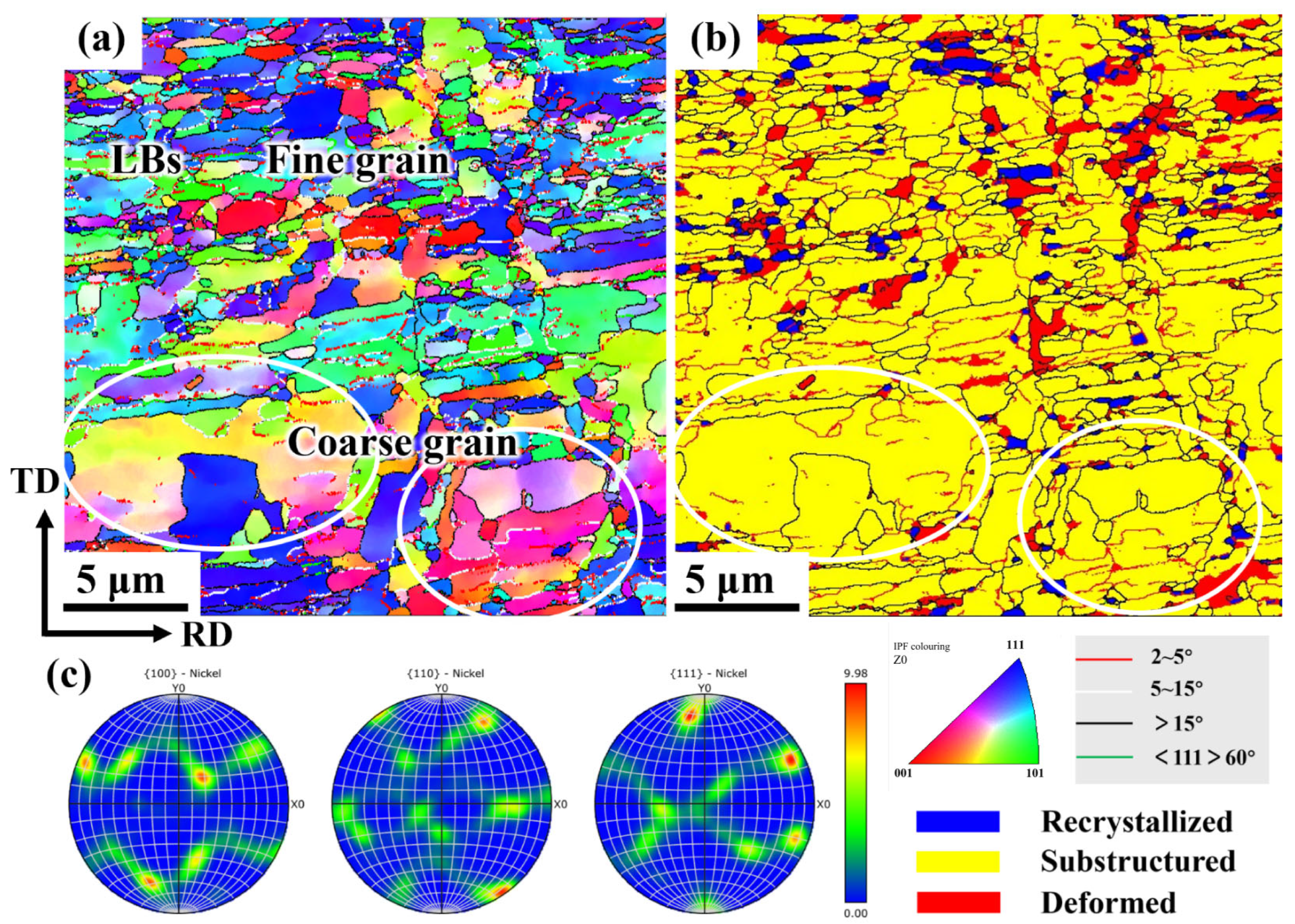
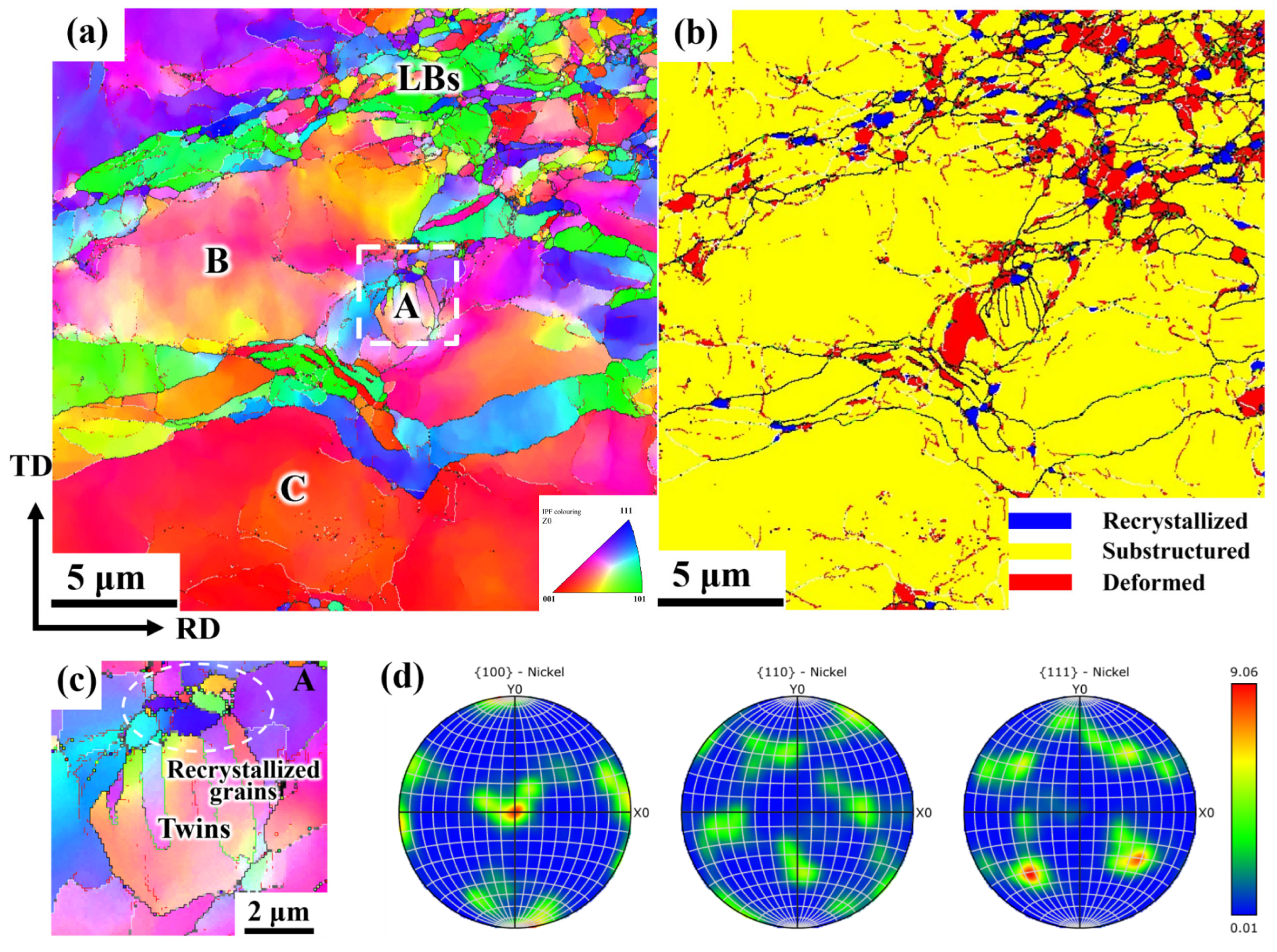
Figure 3 presents the EBSD diagram of multi-channel CR 70%.
As shown in
Figure 3a, the microstructure of CR 70% is divided into fine-grained and coarse-grained regions. The grains in the fine-grained region are elongated along the primary strain direction, resulting in a significant increase in the aspect ratio of the grains. A large number of lamellar boundaries (LBs) were observed during large deformation, and fibrous structures emerged after the full development of the layered organizational structure. The grain size in the coarse-grained region is approximately 5 μm or larger, with some elongated grains also distributed between the large grains.
From the recrystallization diagram (
Figure 3b), it can be observed that a significant amount of recovery occurred in the microstructure of CR 70%, with a small number of recrystallized grains observed between the deformed grains and the recovery substructure. Deformed grains are more prevalent in the fine-grained region, while the coarse-grained region is predominantly composed of recovery substructures. When the CR reached 70% (
Figure 3c), the grains displayed a distinct preferred orientation, primarily S texture, with a minor amount of Brass texture. Dislocation slip, which dominates plastic deformation, typically leads to lattice rotation, causing changes in the texture of the material.
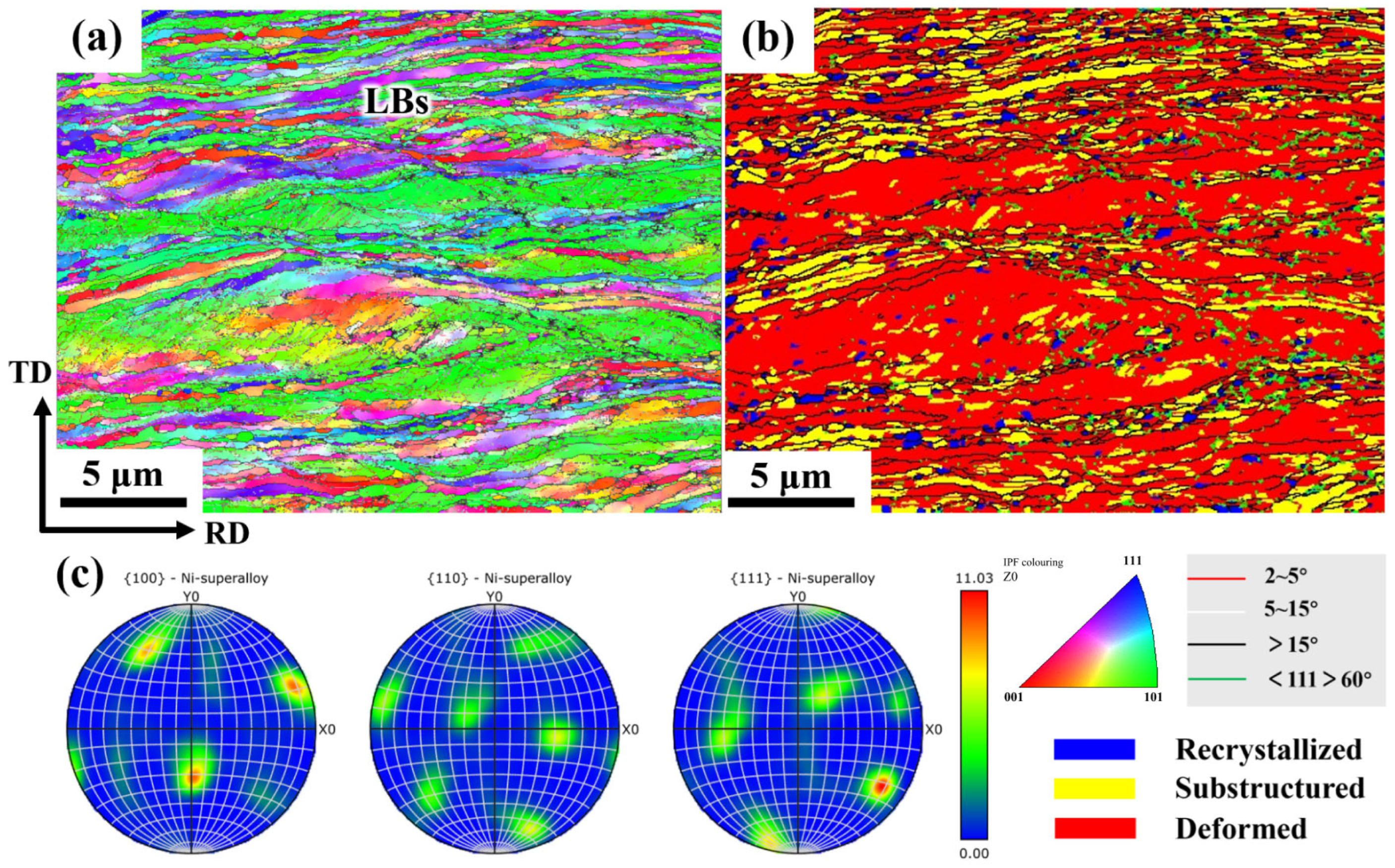
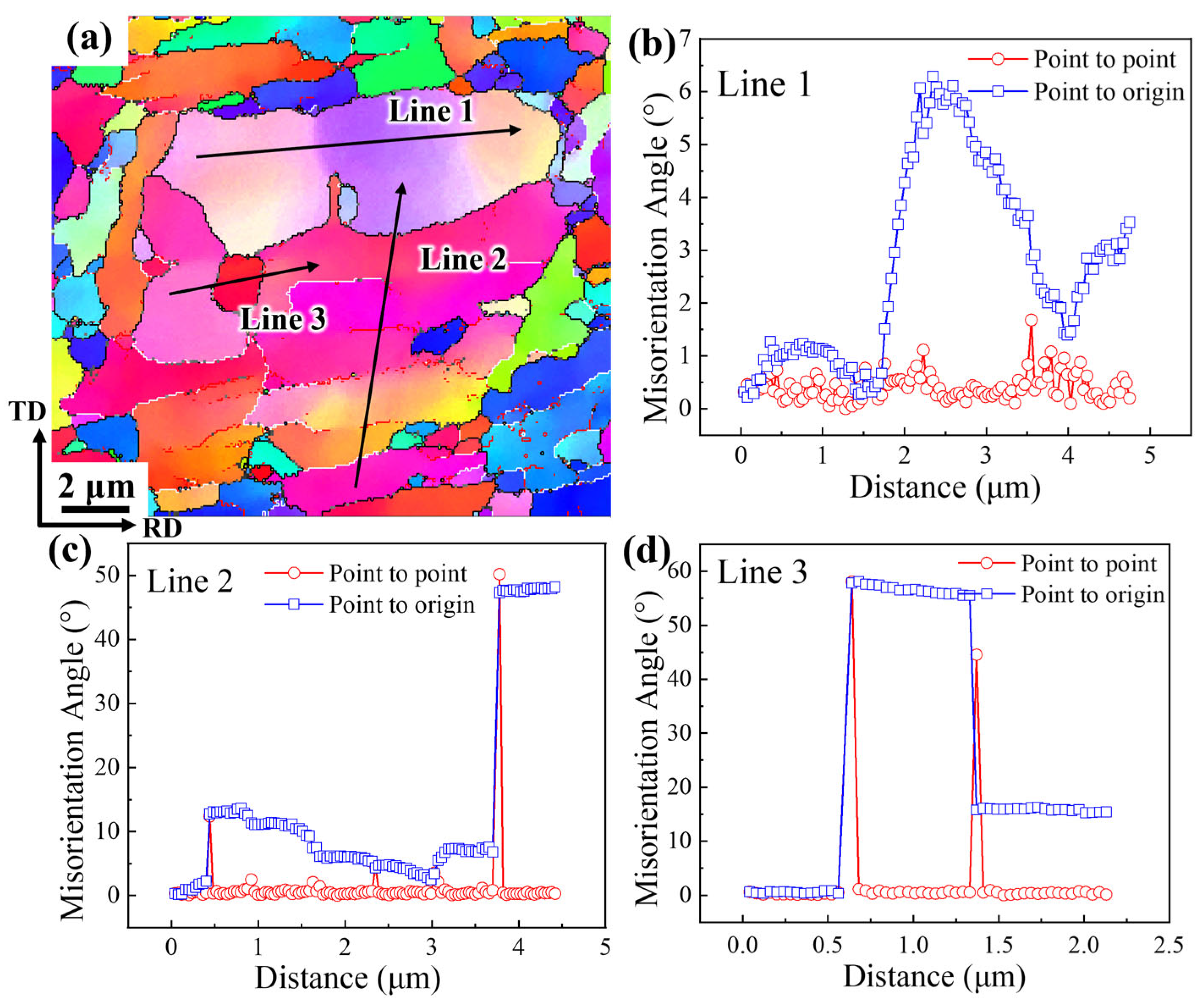
As the deformation progressed, in the cold-rolled sample with CR 90% (
Figure 4a), the grains were significantly refined and elongated, and the aspect ratio of the grains was greatly enhanced. The development of the LBs interface structure reached its peak among the microstructures.
Figure 4b shows that the microstructure contains a large number of deformed structures, with some recovery structures present between the deformed areas, while recrystallized structures are sparse and scattered. With further deformation, the preferred orientation of the electrolytic nickel grains becomes more pronounced, while almost all of them transform into the S texture (
Figure 4c).
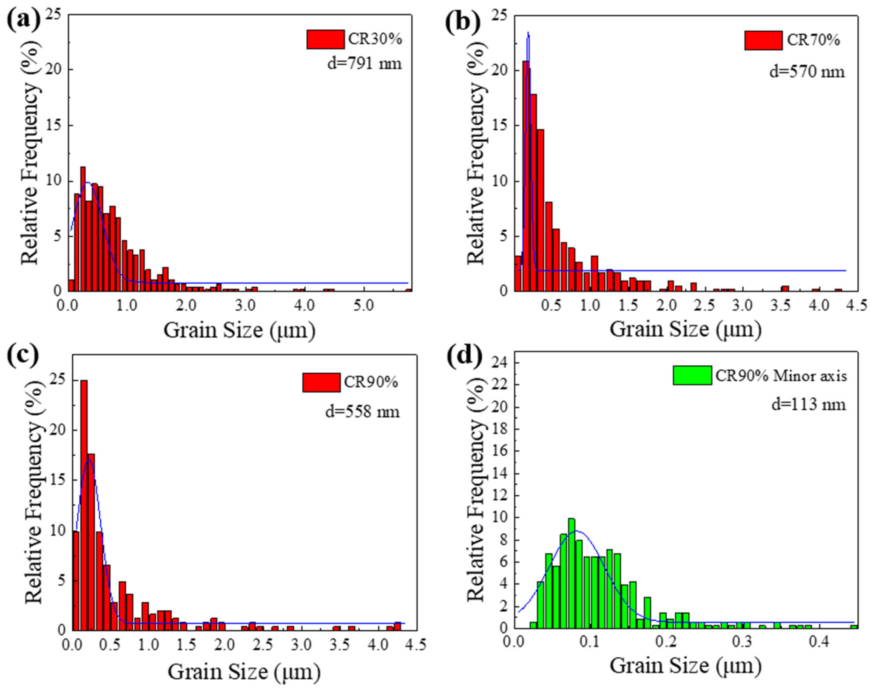
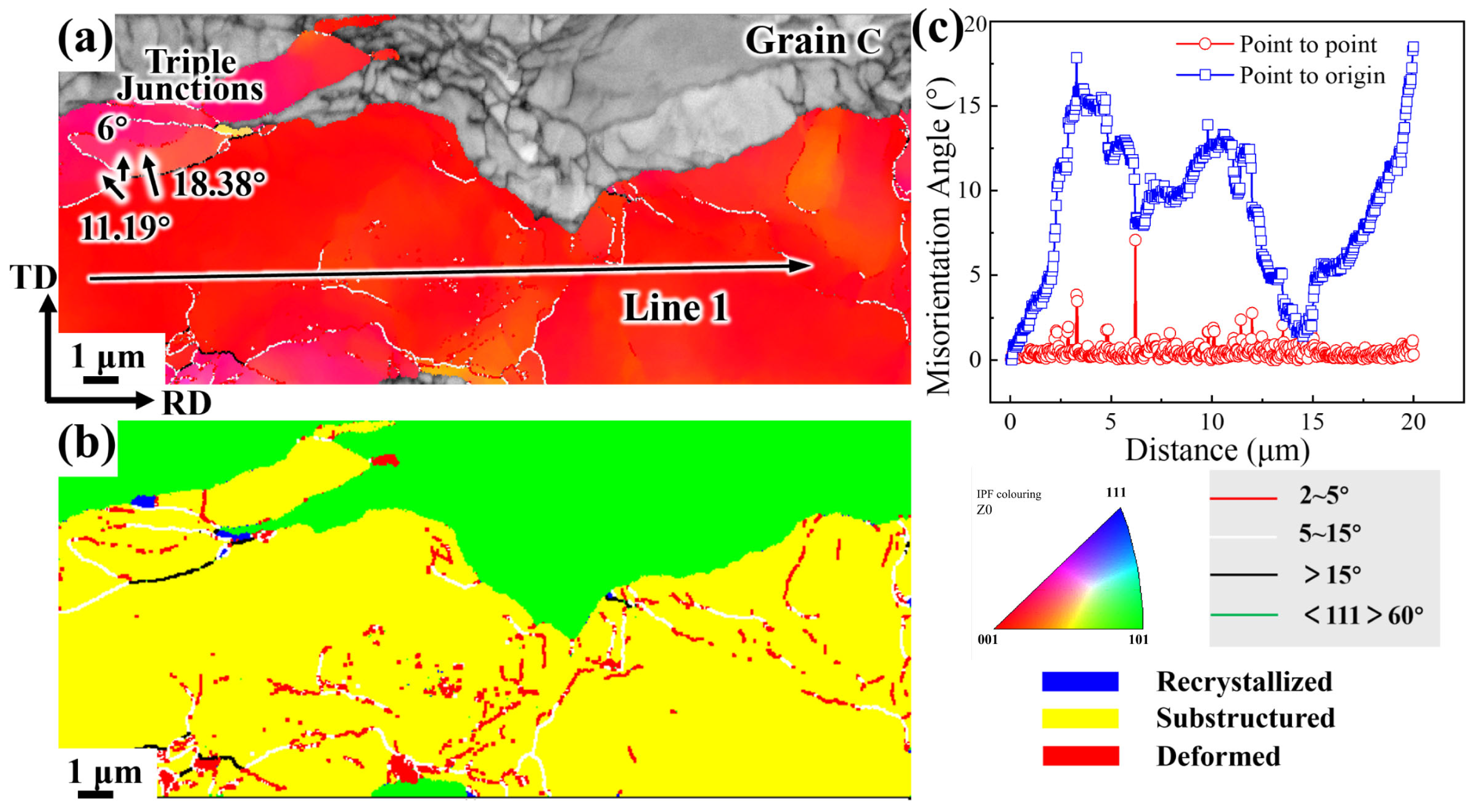
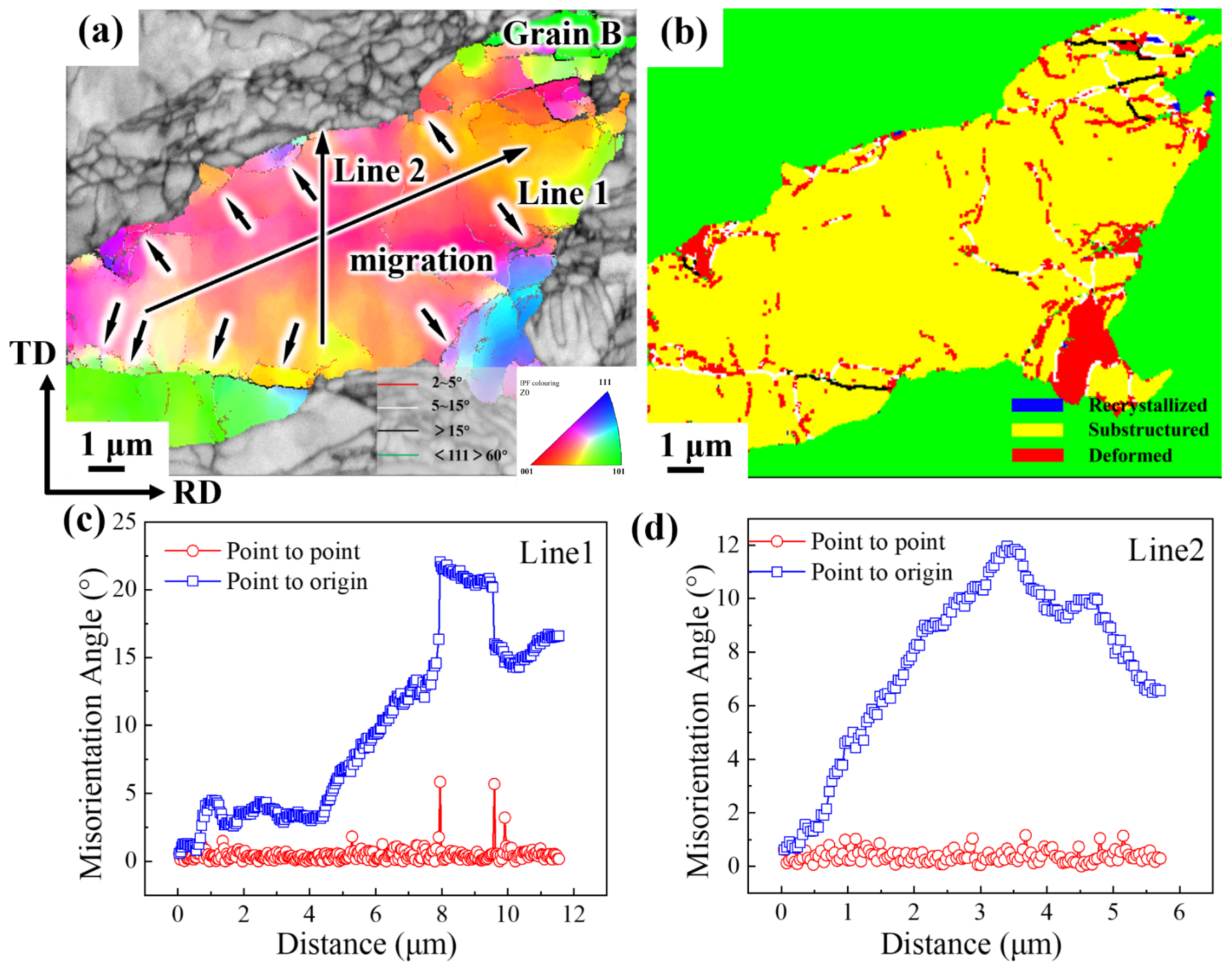
Figure 5 shows that when electrolytic nickel undergoes 98% CR deformation, it is still affected by strain and maintains the typical LBs structure under large strain, although some changes have occurred in its microstructure, with large grains exceeding 10 μm in size appearing (
Figure 5a). The grains in the deformed structure region remain fine, while recovery structures have emerged in some areas (
Figure 5b). During the CR process, electrolytic nickel was not annealed, but dynamic recovery occurred in certain regions of the material. This is due to the uneven deformation during the CR process, with areas of high deformation rates and large deformation amounts, resulting in adiabatic phenomena. The local temperature increased too rapidly and excessively, leading to dynamic recovery.
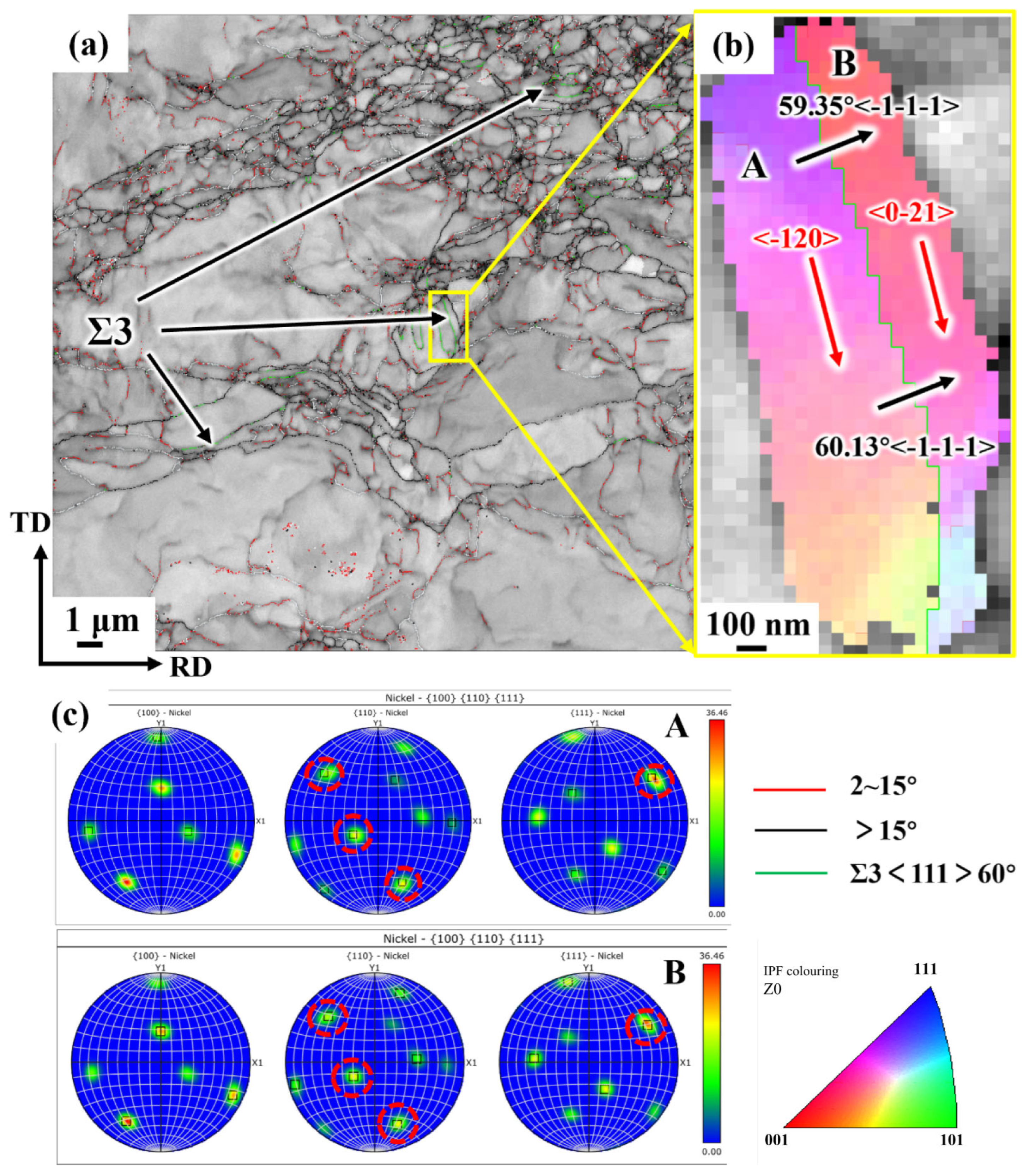
A close-up view of area A in
Figure 5a (
Figure 5c) reveals the formation of an equiaxed grain structure, within grains enclosed by <111> 60° grain boundaries, indicating the presence of twins. During the cold deformation process, with a deformation degree as high as 98%, all grains are affected by large strain, becoming flattened, elongated, and refined. The appearance of equiaxed crystals at this stage suggests that some uncommon phenomena have occurred in these regions, such as recovery recrystallization due to thermal effects. Similar occurrences have been reported in pure nickel subjected to high-pressure torsional (HPT) deformation [
18]. In electrolytic nickel with 98% CR, deformable textures dominated by Brass and S, as well as a small amount of recrystallized textures, including Cube and R, were observed (
Figure 5d).
3.3. Microstructure Evolution of Cold Rolling and the Regression Mechanism of Growth Twins of Electrolytic Nickel Under Small Deformation
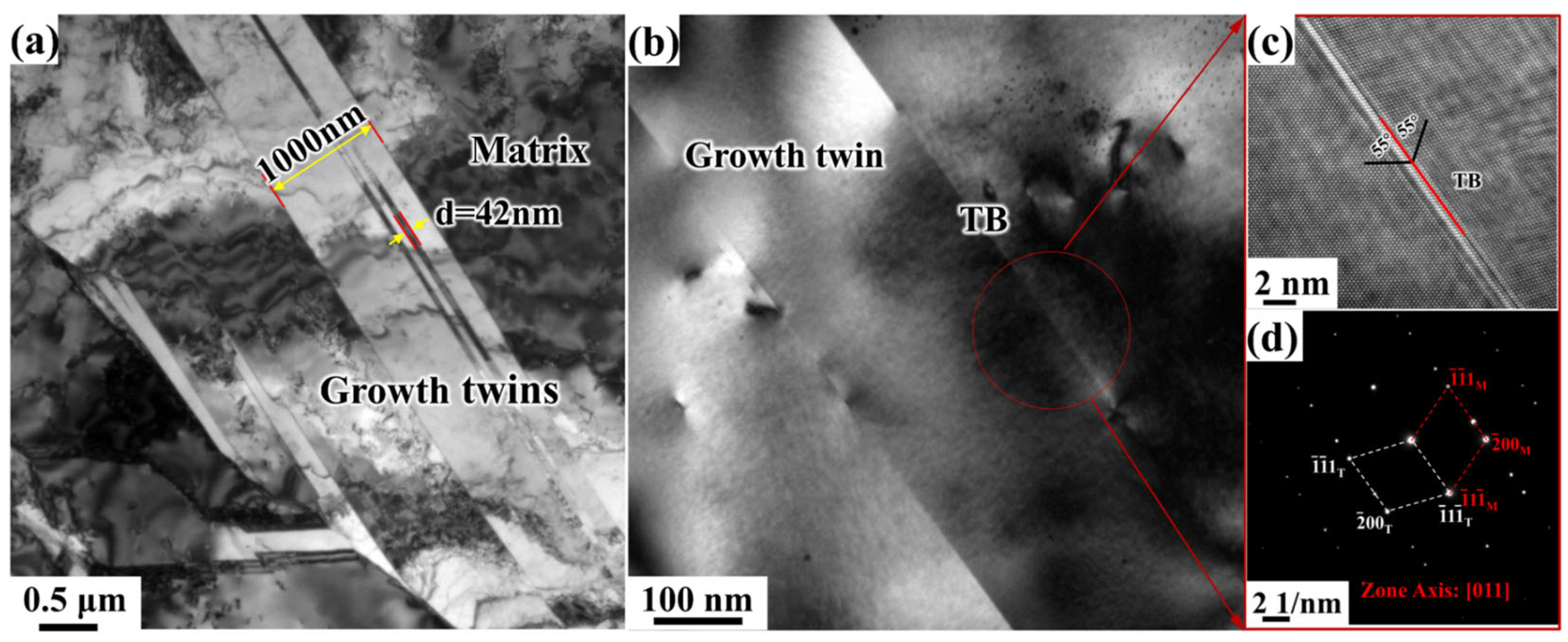
Figure 8 shows the TEM (Transmission electron microscope) morphology of the deposited electrolytic nickel sample. As seen in
Figure 8a, the grain size is highly nonuniform and contains numerous randomly oriented lamellar structures. The HRTEM image of the grain boundaries in
Figure 8b and its magnified view in
Figure 8c, along with the corresponding selected area electron diffraction (SAED) pattern in (
Figure 8d, confirm that the grain boundaries of the lamellar structure are CTBs (Coherent twin boundaries), with a few dislocations observed within the crystal matrix. Additionally, the distribution of the twinned layers is uneven and varies significantly in size. Specifically, the maximum twin length exceeds 20 μm, while the thickness of the layers ranges from several tens of nanometers to approximately 1000 nm.
For metals with medium to high stacking fault energies, the formation of growth twins is typically difficult. In most pure nickel systems, twinning generally occurs through annealing processes. Previous studies have shown that when thick films are fabricated by magnetron sputtering, both pure and Al-doped nickel can exhibit nanoscale TBs [
21,
29,
30]. The occurrence of a high density of growth twins in electrodeposited pure nickel is largely attributed to the presence of impurity elements in the electrolytic nickel [
31,
32]. This industrial-grade electrolytic nickel exhibits a wide grain size distribution, with the coexistence of micro- and nano-sized grains and a high density of growth twins. The microstructure of this bulk electrodeposited metal is thus highly complex, which will have a profound and multifaceted impact on its plastic deformation behavior.
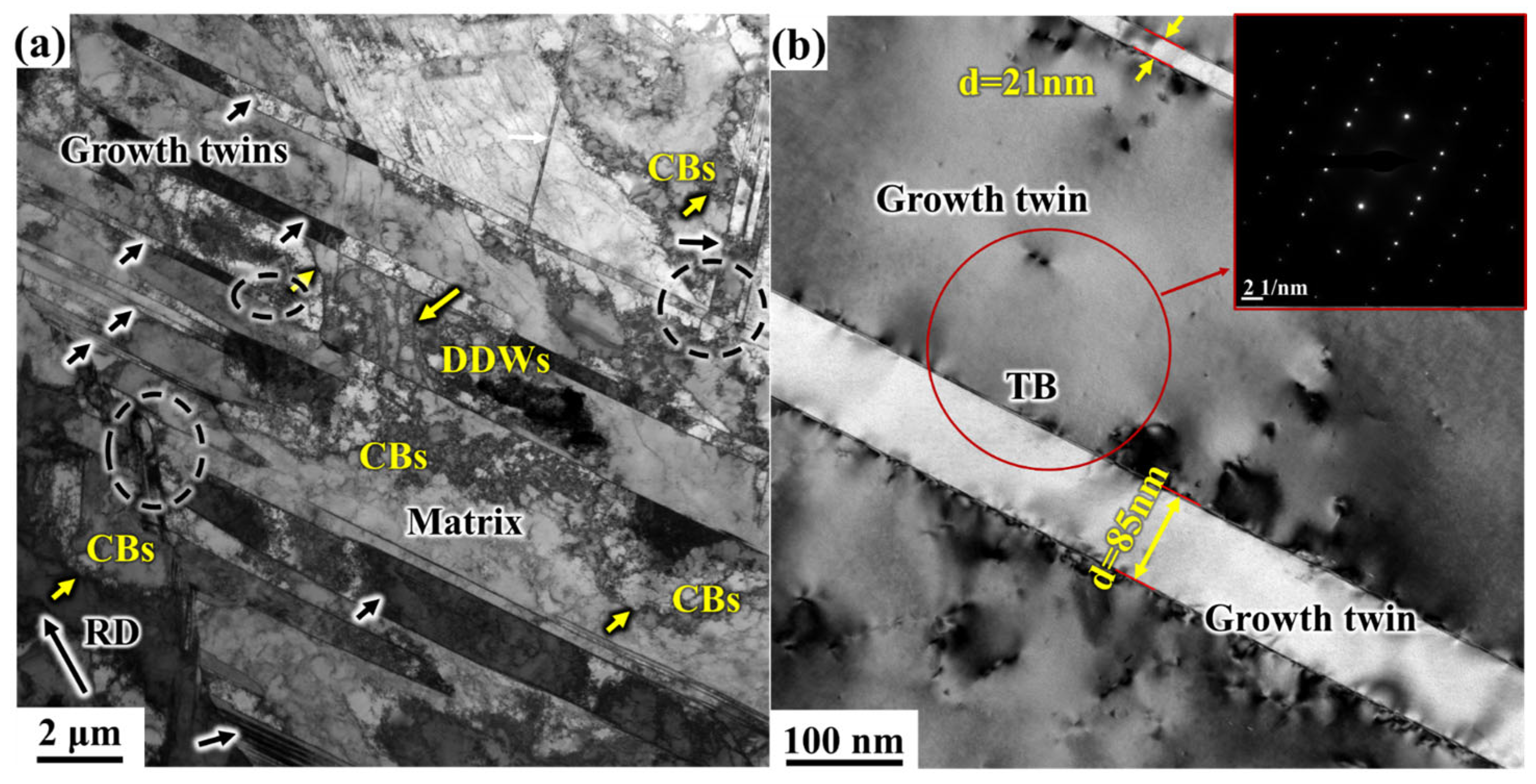
Figure 9 illustrates the transmission electron microstructure of the electrolytic nickel sample after CR 5%. At this stage, although the deformation is minimal, meaning that the electrolytic nickel has only just begun to experience deformation, dislocations can be observed to appear rapidly within its internal structure (
Figure 9a). These dislocations accumulate and settle into dislocation interfaces during the plastic deformation process, subdividing the grains into cells and CBs with different structures [
33]. At low strain, long, and straight dislocation interfaces (DDWs, Density dislocation walls) gradually form, segmenting the grains into different CBs (Cell blocks), which help accommodate the strain of adjacent cell blocks. Geometrically necessary boundaries (GNBs) [
20,
34] are also formed between the CBs. These interfaces arise from the interaction of dislocations in different slip systems, facilitating the coordination of inhomogeneous deformation.
At this stage, the growth twin boundaries that formed during the nickel electrodeposition process remain clearly visible (
Figure 9b), and the corresponding SAED patterns indicate that the twin orientation relationship has not changed. It is observed that in the figure, one twinned layer has a thickness of 21 nm, while another has a thickness of 85 nm.
During the CR process, the grains within electrolytic nickel are gradually elongated due to the rolling deformation, and local areas begin to deform. These areas are also affected by strain, causing the torsion angles of grains with different orientations to vary. Due to the anisotropy of plastic deformation, dislocations preferentially propagate along the twin boundaries [
35]. Dislocations on TBs and within the twins begin to proliferate rapidly. Twinned lamellae aligned with the rolling strain direction experience minimal change, while those at 45° or other orientations are more affected. Some twin layers with different directions begin to interact, as indicated by the circular area in
Figure 9a.
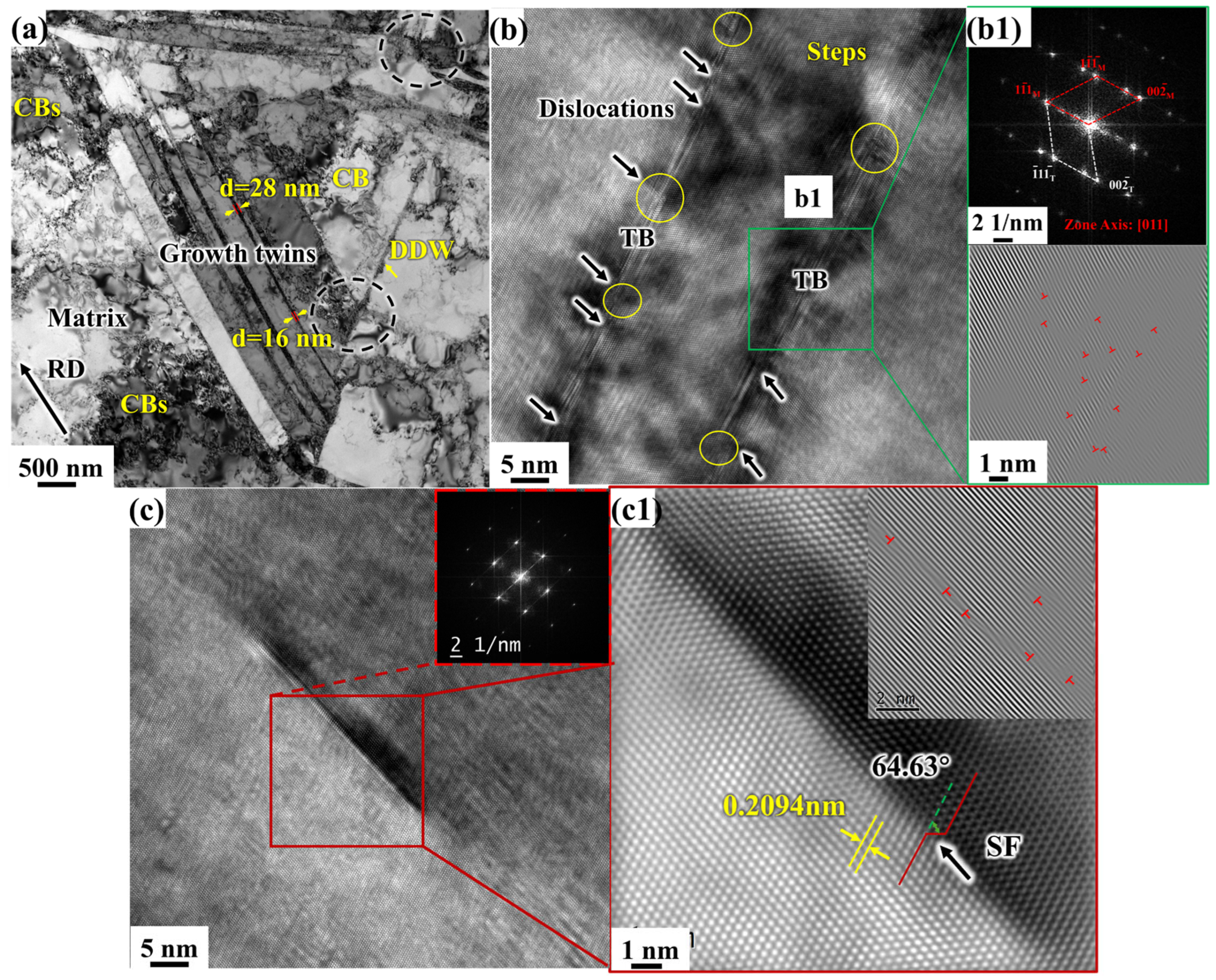
Figure 10 presents the TEM microstructure of the 10% CR sample. Although the deformation at 10% is small, the TBs are inevitably affected by dislocation movement, and dislocations are emitted along the TBs. As shown in
Figure 10a, with increased deformation, dislocations in the internal structure continue to proliferate, and the formation rate of dislocation cells accelerates. More growth twins squeeze the surrounding matrix structure, and further cuttings occurs between the twinned lamellae (indicated by the circular area in
Figure 10a). Growth twins in different directions are affected by strain, leading to elongation and bending. Twins along the direction of maximum shear stress exhibit significant bending, while those parallel to the rolling direction become elongated and thinner. The thickness of the same twinned layer changes from 28 nm to 16 nm, as twinning is influenced by deformation, resulting in an increase in length and a decrease in thickness (
Figure 10a).
The originally straight TBs gradually exhibit evolutionary characteristics as deformation progresses. The TBs undergone significant shear deformation. In
Figure 10b, a large number of dislocations accumulate along the TBs. TBs that are perpendicular or inclined at a certain angle to the strain dislocate more rapidly, resulting in the formation of multiple steps. These steps progressively divide the grain boundaries until they are sheared off. Subsequently, the TBs that were cut off break into sections of interfaces (
Figure 10b). However, due to the small amount of deformation at this stage, most areas still maintain a well-defined twinned lamellar structure, and the corresponding SAED pattern (
Figure 10b1) indicates that the twin relationship has not changed.
As the deformation progresses, more dislocations become entangled into clusters, leading to a dense packing of dislocations. The sawtooth pattern of the TBs intensifies, eventually blurring the growth twin boundaries. Dislocations produced and emitted by the TBs gradually expand into the crystal matrix, forming numerous dislocation cells within the twins. Stacking faults (SFs) were observed in the deformed microstructure of electrolytic nickel at small strains, as shown in
Figure 10c. Similar to the twinning phenomenon in pure nickel, delamination is less likely to occur. At this stage, the occurrence of layer faults may be linked to the high number of growth twins formed during electrodeposition.
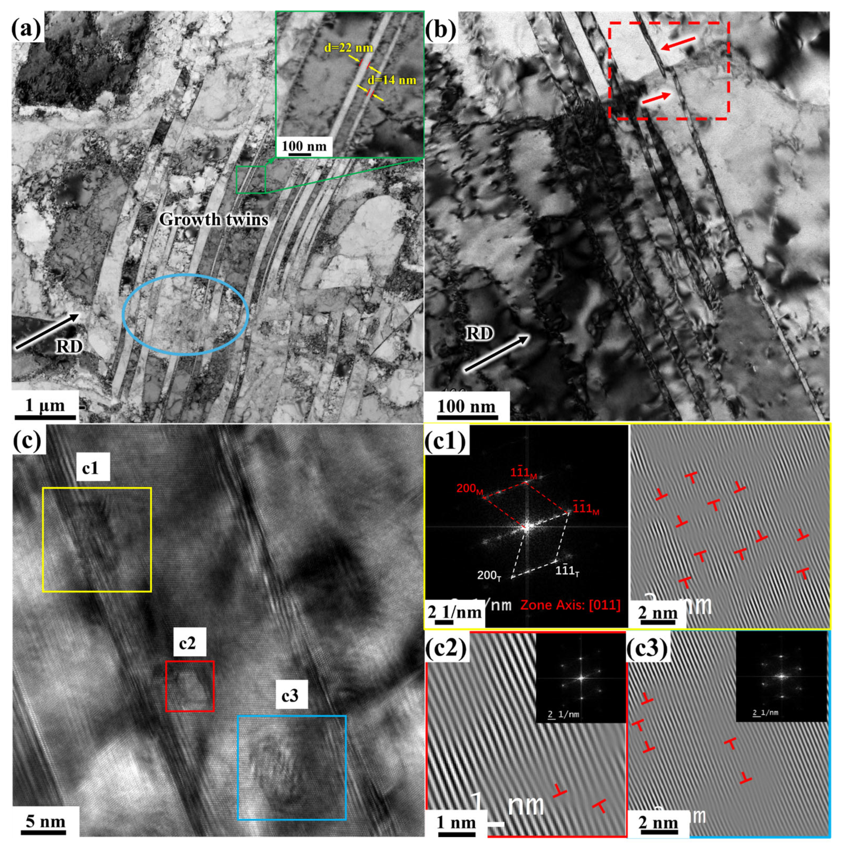
Figure 11 shows the microstructure of the 30% CR sample. As shown in
Figure 11a, with increasing strain, the twinned layers continue to elongate, and their curvature becomes more pronounced. One twin is observed to be 22 nm thick, while another is only 14 nm thick, indicating that the growth twins are continuously elongated and thinned under strain. A large number of dislocations accumulate near the TBs, which differs from the initial state of straight, clean growth twin boundaries before deformation. Large twinned lamellae can accommodate shear strain through intragastric dislocation motion, while fine twinned lamellae, due to the size limitation of dislocation movement, cannot coordinate shear strain through dislocation motion alone. Instead, they accommodate shear strain through dislocations and TBs reaction-induced detwinning. A large number of dislocations interacting with the TBs induce continuous dislocation reactions, causing a significant proliferation of dislocations along the TBs and their accumulation, resulting in twin bending. At the shear strain concentration point, the growth twins in the electrolytic nickel have started to fade, as shown in the circular area of
Figure 11a. Multiple twinned lamellae become difficult to distinguish, and the twin boundaries are completely blurred.
As shown in
Figure 11b, a large number of dislocations are entangled within the growth-twinned lamellae. Under the influence of local strain, dislocations accumulate in a direction perpendicular to the twin boundaries, causing multiple twins to collectively deflect. Due to the deformation, the twinned lamellae not only bent but also experience breakage. A twinned lamella completely disconnected by dislocation cutting was observed (at the position marked by the short dashed box in
Figure 11b).
Figure 11c shows the characterization of the twinned microstructure by HRTEM. The diffraction pattern corresponding to the c1 grain boundary in the figure still maintains the twin relationship, though it slightly deviates from the original crystal band axis. This indicates that only a small deflection has occurred in the orientation between the twin and the matrix. On these incompletely dissipated twins, dislocations continue to be emitted from the TBs, proliferating and moving near the twin boundaries until they accumulate and entangle. The dislocation density near the TBs increases progressively. As strain increases, new slip systems are activated to coordinate the deformation. During the continuous movement of dislocations, the TBs can no longer impede dislocation motion, resulting in a large number of movable incomplete dislocations on the TBs. Under the mutual interaction of dislocations and TBs, the originally continuous and straight TBs become discontinuous and eventually break under continuous strain. The original growth twins in electrolytic nickel soon disappear.
Under dislocation motion, different regions of the twins undergo various changes. The unique mechanical behavior of twins stems from their inherent deformation mechanisms. Research [
36,
37] indicates that when an edge dislocation encounters Σ3 TBs, the interaction between the dislocation and the TBs generates a new edge dislocation, which can slip within the twinned lamellae. Simultaneously, a new incomplete dislocation is created at the TBs, which can also slide along the TBs. In this manner, the original growth-twinned lamellae in electrolytic nickel not only impede dislocation motion but also act as slip planes for dislocations, absorbing and storing dislocations during deformation. This mechanism strengthens the metallic material while improving its macroscopic plasticity [
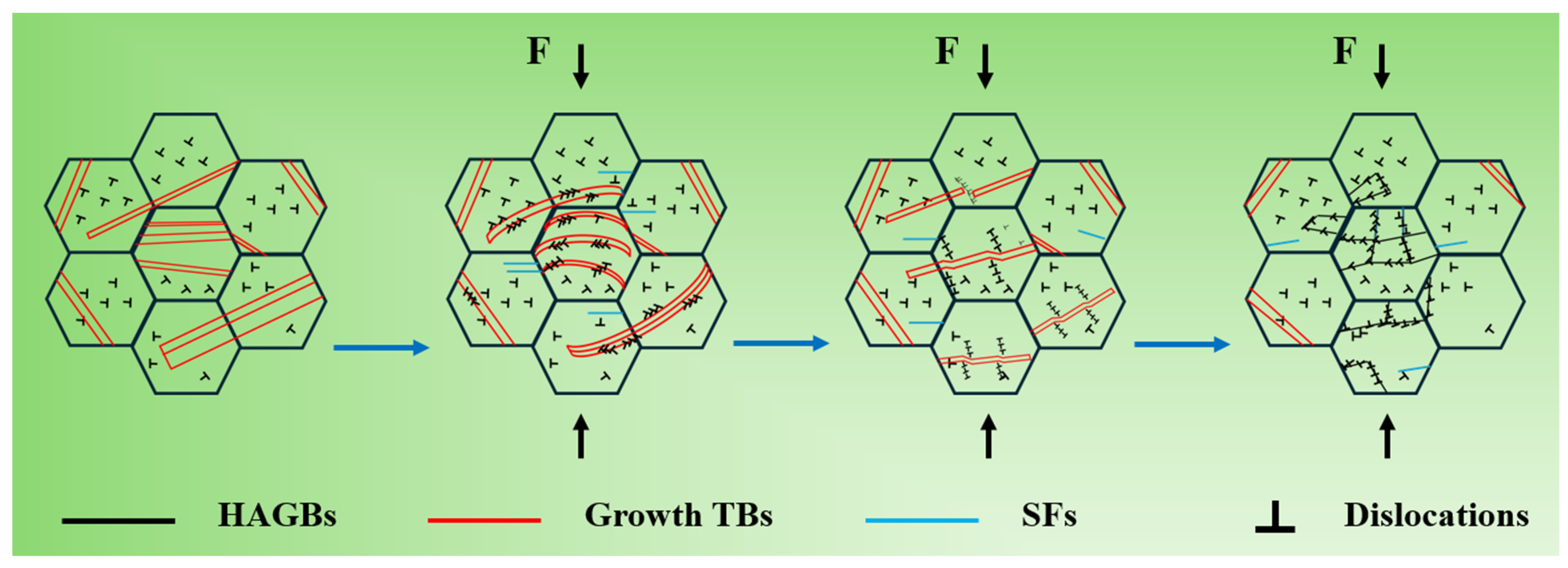
38]. Thus, under CR conditions, during the initial stage of deformation of electrolytic nickel, the plastic deformation is predominantly governed by the detwinning mechanism, which involves extensive interaction between dislocations and twins. A schematic diagram of this mechanism is shown in
Figure 12.
3.4. Evolution of Cold-Rolled Microstructure and Cold Plastic Deformation Mechanism Under Large Deformation
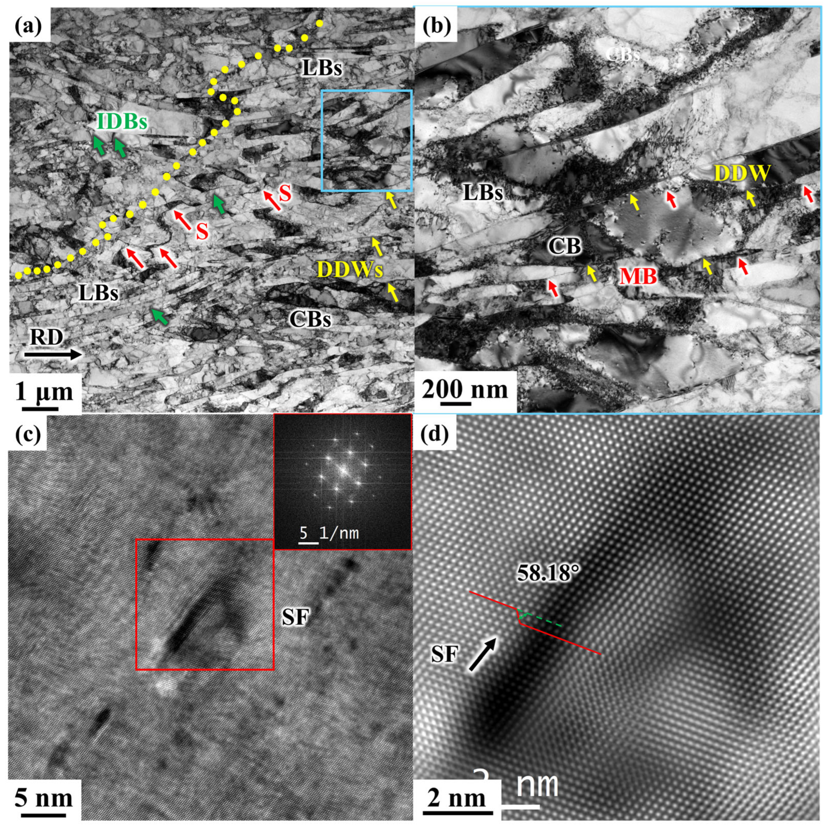
After 70% deformation in CR, the deformed structure is shown in
Figure 13. As shown in
Figure 13a, with increasing deformation, the number of dislocation cells increases, the grains become progressively finer, and dislocation proliferation continuously enhances the strength of the material. These fine grains are formed through the evolution of dislocation structures and the shearing and fragmentation of growth twins. S-bands are also observed (indicated by the red arrows in
Figure 13a), which from when intense shear occurs due to local large shear strains. At 70% CR, the deformation degree transitions from medium strain to large strain, and at this point, the microstructure contains both typical small-strain and large-strain structures, making the deformation structures in the CR 70% microstructure highly diverse.
During plastic deformation of metals, different CBs form within the grains, and slight orientation differences between these cell blocks result in variations in the slip systems activated by each block. The interface structure of DDWs/MBs (Microbands)/LBs forms GNBs, while the boundaries of dislocation cells and the interfaces between layered interfaces are classified as IDBs (Incidental dislocation boundaries), as indicated by the green arrow in
Figure 13a). IDBs are dispersed interfaces located between GNBs and retain distinct dislocation characteristics. The interaction between dislocations within the cell blocks constantly generates new IDBs as strain increases from small to large.
The lamellar structure, often referred to as LBs, gradually forms when metals undergo large strains, as shown in
Figure 13a. This structure is composed of DDWs and CBs, and is a characteristic feature of medium- to high-energy metals under significant deformation [
20]. Each layer contains several cell blocks. As stress increases, individual DDWs gradually widen and start to split into two or more DDWs. The splitting of original DDWs is the most common mechanism for the formation of new CBs. After splitting, DDWs exhibit strip-shaped morphological characteristics under a transmission electron microscope, which are known as MBs, as shown in
Figure 13b.
FCC metals have multiple slip systems, but pure nickel is not prone to twin deformation during plastic deformation. Only under low-temperature and high-strain rate conditions, when dislocation motion is hindered, can a deformed twin structure form [
35]. After 70% CR deformation, it is difficult to observe the presence of twin boundaries in the microstructure of electrolytic nickel. The growth twins essentially disappear under the influence of large deformation. Consequently, the electrolytic nickel, which initially contained a large number of growth twins, not only sees the disappearance of growth twin post-deformation but also shows minimal appearance of deformation twins. Under 70% large strain, a significant number of laminar structures appear in the electrolytic nickel microstructure (
Figure 13c). During the cold deformation process of electrolytic nickel, the deformation mechanism is characterized by the coexistence of dislocation slip and dislocation interaction.
After 70% deformation by CR, the microstructure transitions from MBs/DDWs inclined towards the rolling plane to LBs nearly parallel to the rolling direction.
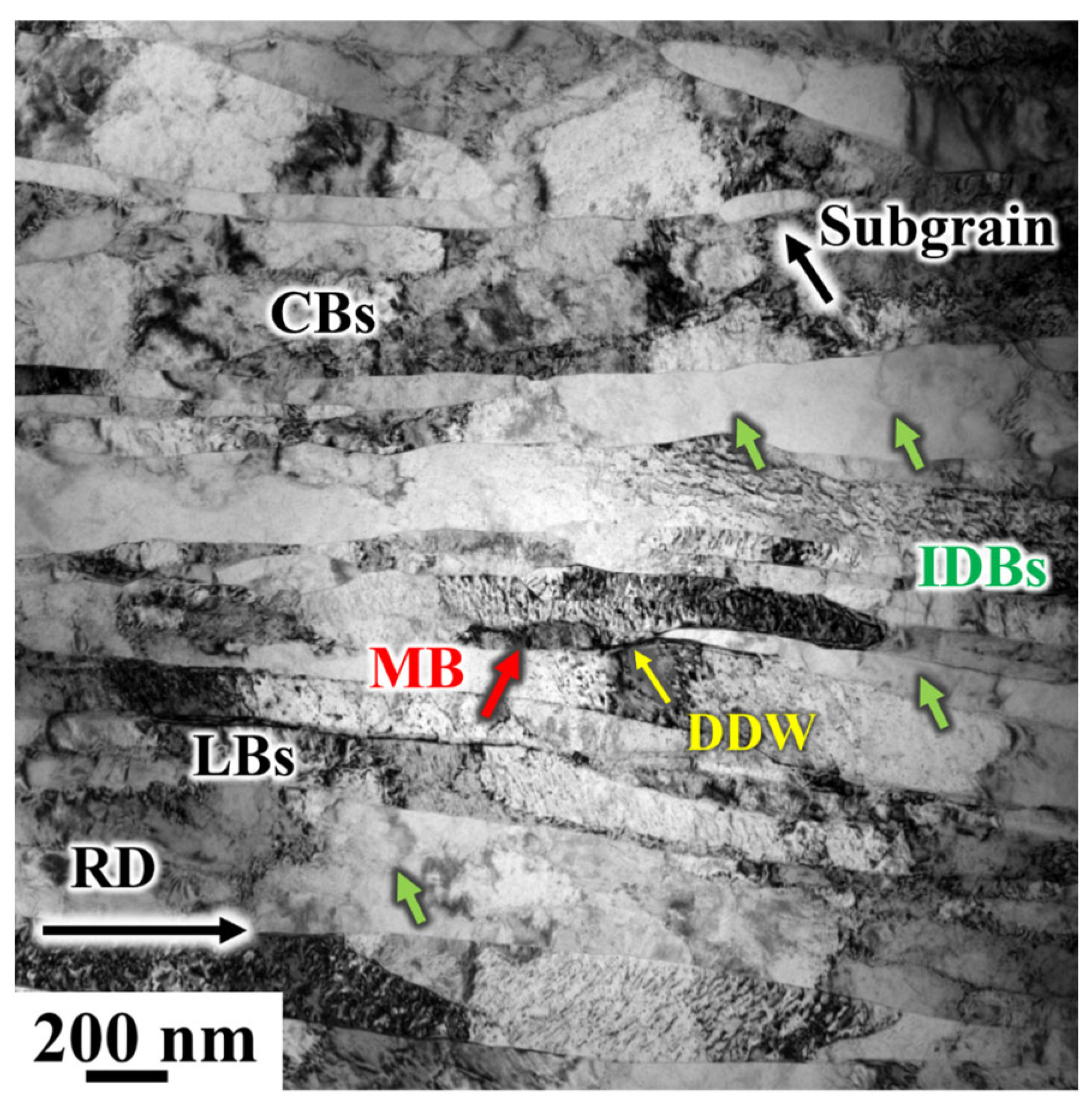
Figure 14 shows the microstructure of the CR 90% sample, where the microstructure has almost entirely evolved into LBs. The width of these LBs ranges from 200 nm to 600 nm. The lamellar structure is not perfectly straight but gradually bends along with local structures or local shear zones.
Under moderate strain, a new dominant slip system rapidly emerges, transforming the structure from one associated with small strain to one characteristic of large strain [
39]. The spacing between IDBs and GNBs continuously decreases as strain increases. The thinned layers continue to deform and are further subdivided by IDBs into the typical high-strain structure (
Figure 14). Inside the LBs, a large number of entangled dislocations and CBs are observed, while between the layers, a few DDWs and MBs are present.
Under the influence of large strain, due to the movement of dislocations and the interaction between dislocations and laminates, the original CBs gradually elongate and refine into smaller CBs. Simultaneously, the number of MBs increases, and the orientation difference between the matrix and MBs also becomes more pronounced. Ultimately, as cumulative deformation progresses, the MBs further refine and eventually disappear, leading to the formation of subcrystals.
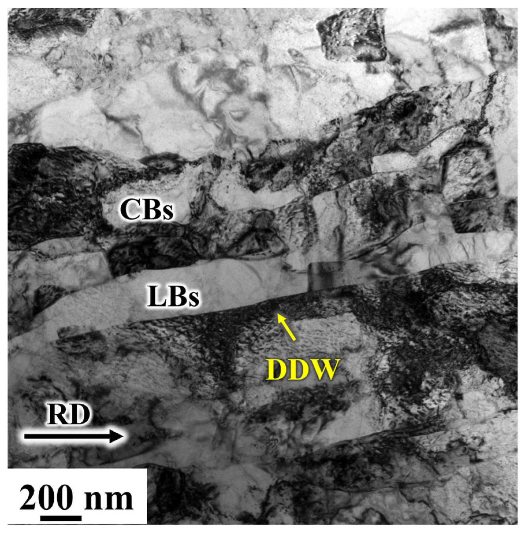
Figure 15 shows the transmission electron microstructure of the sample at CR 98%. The LBs lamellar structure is still visible in the figure, which is thicker compared to the lamellar structure at 90% CR. CBs are also present. With increasing deformation, at CR 98%, the interfacial spacing between the layers did not continue to decrease as observed in polycrystalline nickel at CR 98% [
20], nor did it form large-angle grain boundaries under the combined effects of structural and texture evolution [
40]. Instead, the spacing between the layers increased.
3.6. Microhardness of Electrolytic Nickel at Different Pressing Amounts
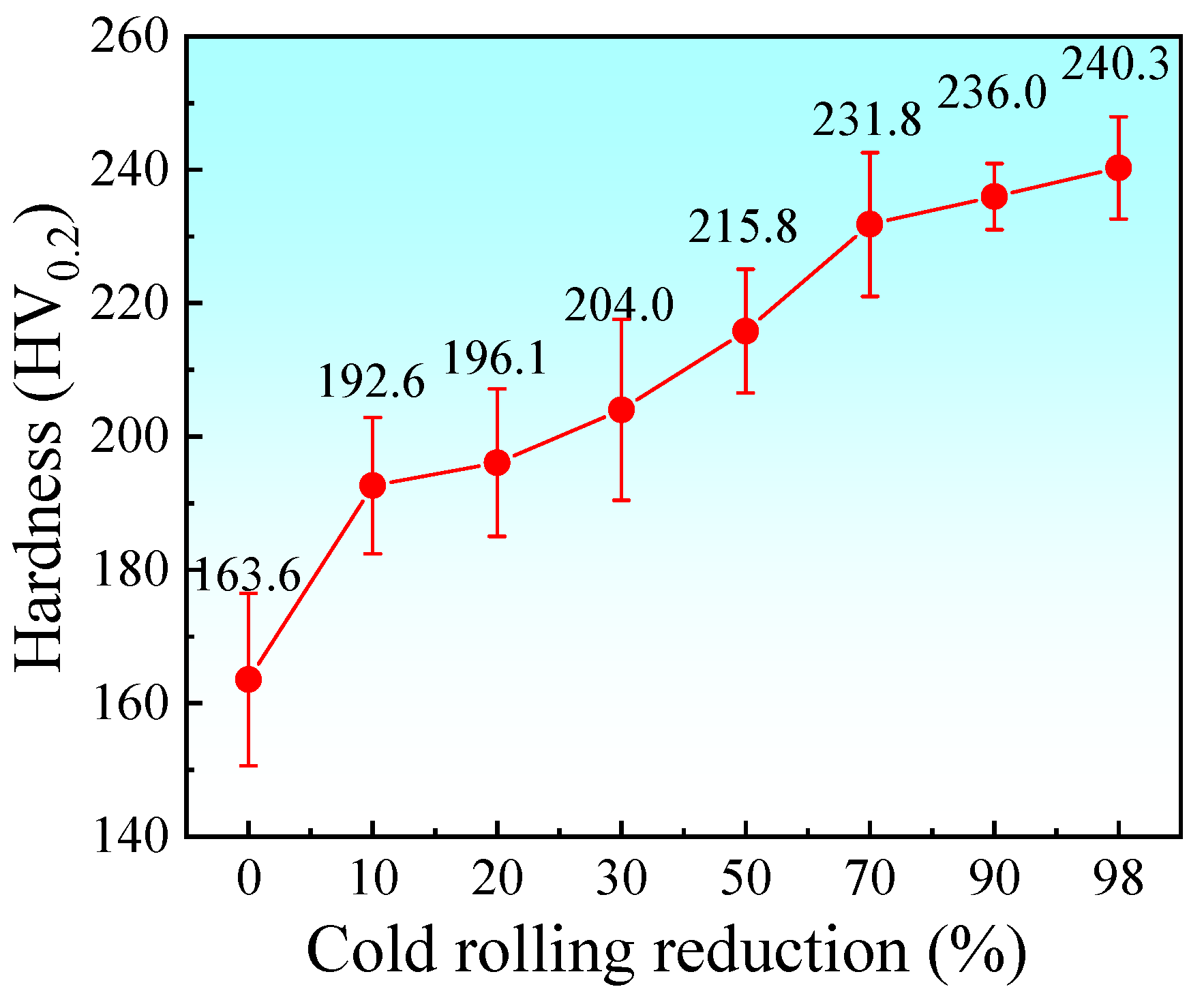
Figure 17 presents the microhardness values of electrolytic nickel after CR with varying degrees of deformation. As the deformation degree increases, the hardness of the electrolytic nickel rises significantly. The average microhardness of the deposited electrolytic nickel is 163.6 HV. After 10% CR, the average microhardness increases from 163.6 HV to over 192 HV. At 30% deformation, the microhardness value reaches 204.0 HV. With a deformation degree of 50%, the average microhardness is 215.8 HV, and the material continues to strengthen. When CR reaches 70%, the average microhardness is 231.8 HV, representing a cumulative increase of more than 41%, with the strengthening rate remaining relatively high.
As deformation continues, the rate of hardness increase begins to decline, and the hardness value shows only a slight rise. This indicates that the microstructure of electrolytic nickel tends toward a relatively stable state with increasing strain. When the CR reduction reaches 98%, the average microhardness attains the maximum value during the entire deformation process, reaching 240.3 HV. Compared with the undeformed state, this corresponds to a cumulative increase of 46.88% in microhardness.
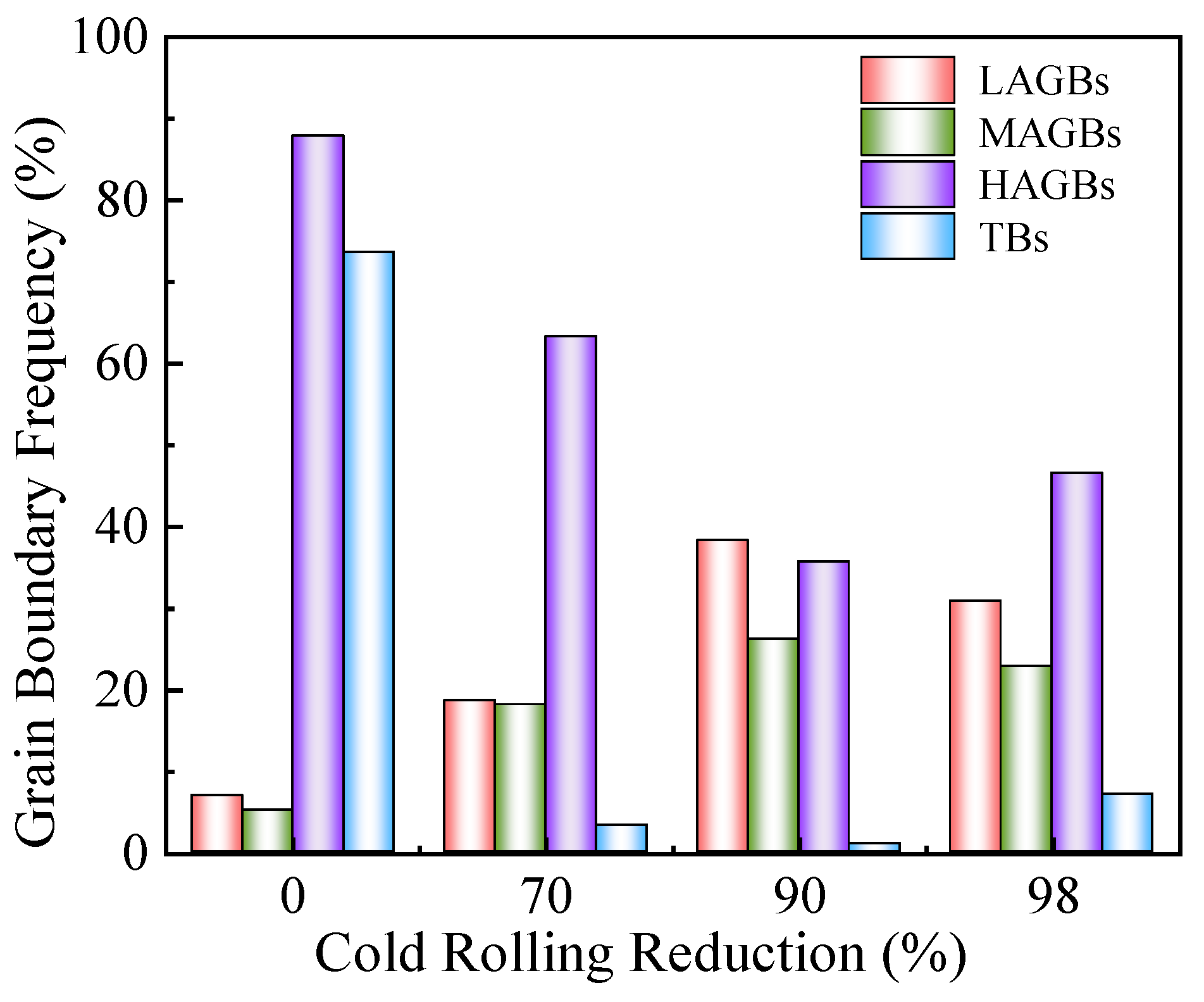
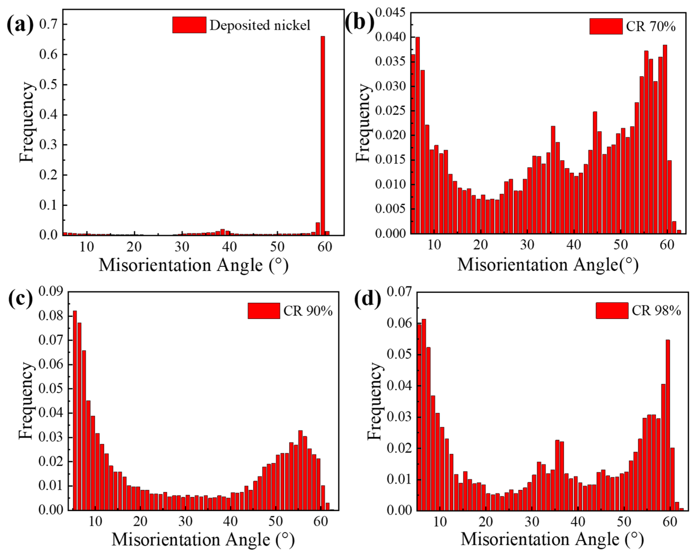
During the cold-rolling-induced strain hardening of electrolytic nickel, the primary microscopic mechanism of strengthening is the accumulation of dislocations at grain boundaries. The resistance to dislocation slip is associated with the interfacial misorientation of small-angle grain boundaries. A larger misorientation results in more significant obstruction to dislocation motion, with a strengthening effect comparable to that of large-angle grain boundaries [
41]. Previous studies [
42] have shown that the critical misorientation angle typically ranges from 2° to 5°. Therefore, as the degree of rolling deformation increases, the proportion of small-angle grain boundaries continuously rises, which is considered the main factor contributing to the rapid increase in the hardness of electrolytic nickel.