
Effect of Substrate Temperature on the Structural, Morphological, and Infrared Optical Properties of KBr Thin Films

 ,
,  , ,
, , Highlights
- Establishing quantitative correlations between deposition temperature and multi-dimensional structural properties, including preferential (200) orientation, stress relaxation, and defect density minimization.
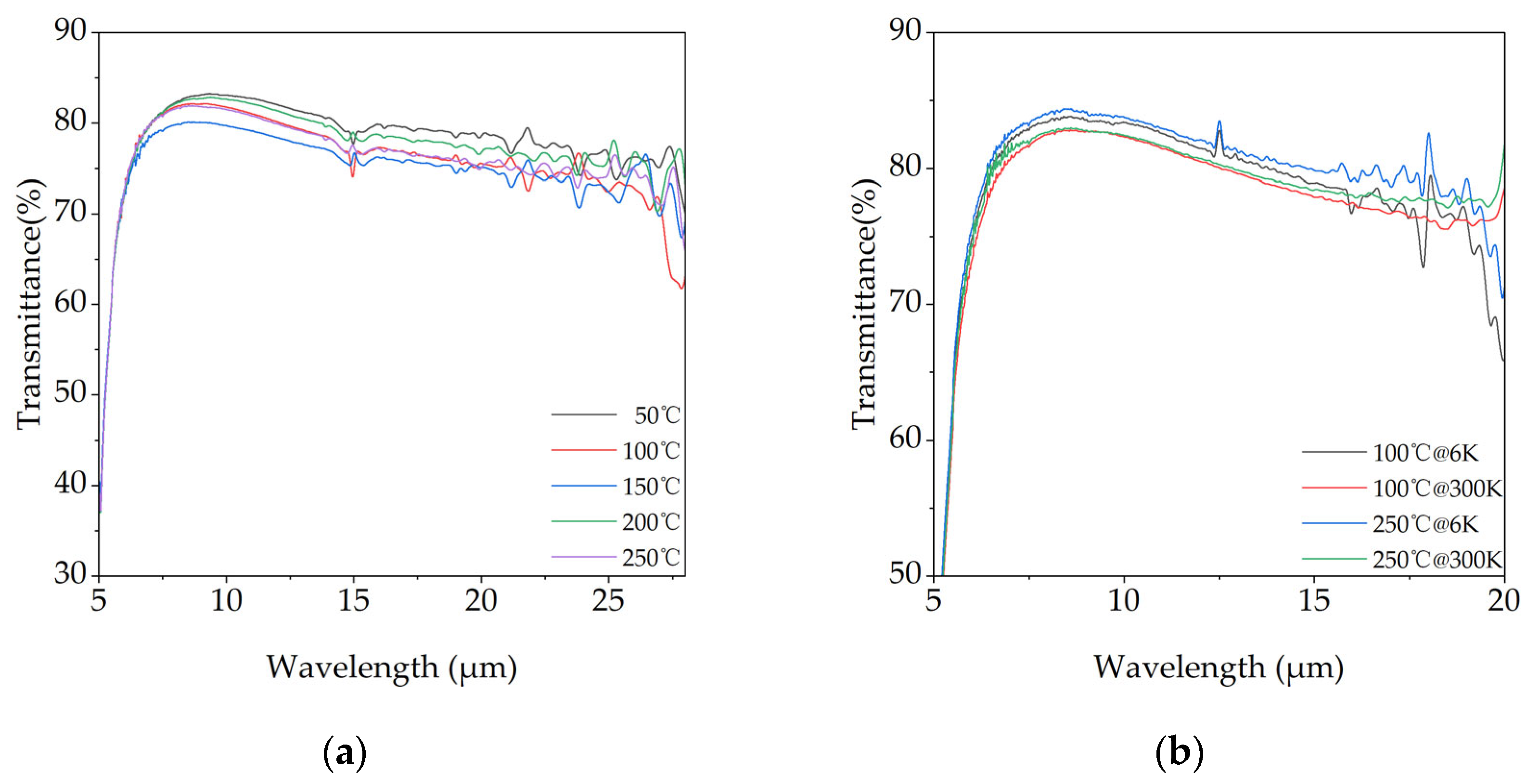
- Providing cryogenic (6K) infrared transmittance data, highlighting the suppression of multi-phonon absorption critical for low-temperature optical systems.
- Delivering practical engineering guidance for the design and optimization of high-performance KBr-based infrared coatings, windows, and filters.
Abstract
1. Introduction
2. Experimental Details
2.1. Sample Preparation
2.2. Film Characterization
3. Results and Discussions
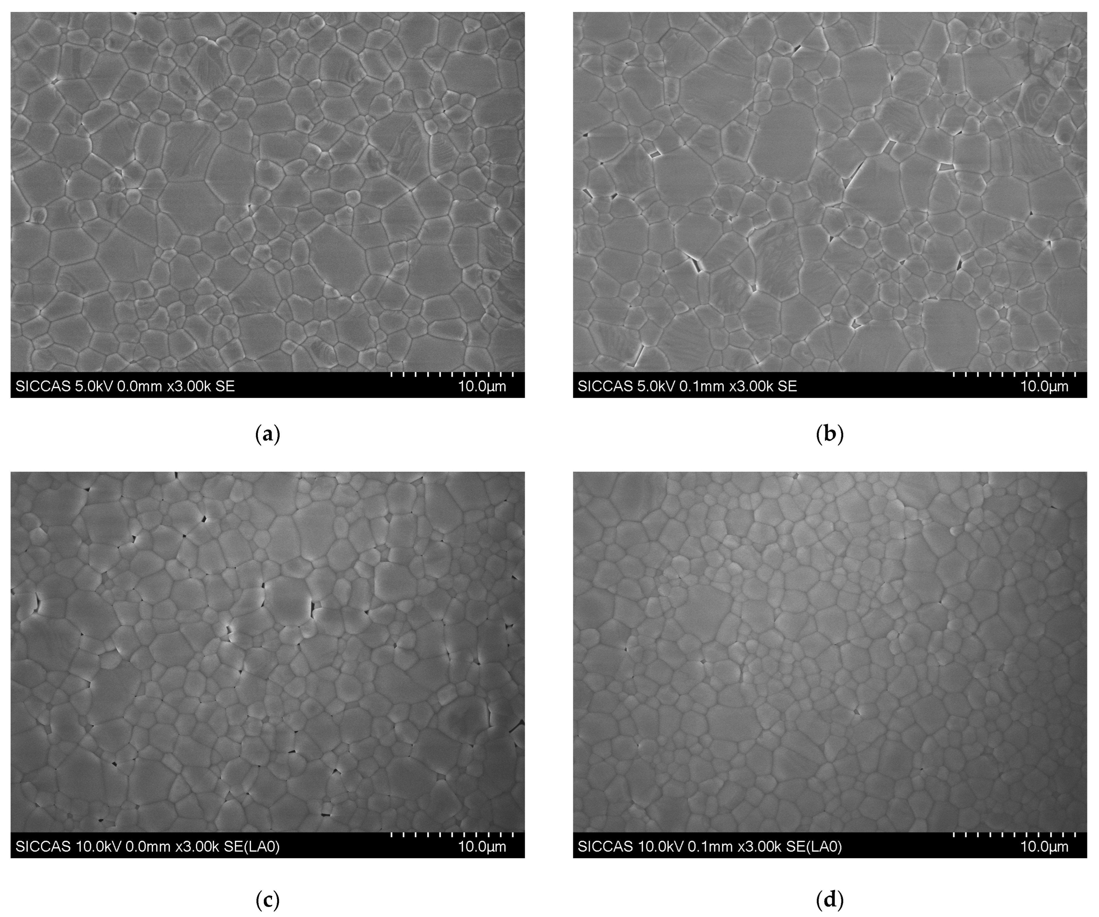
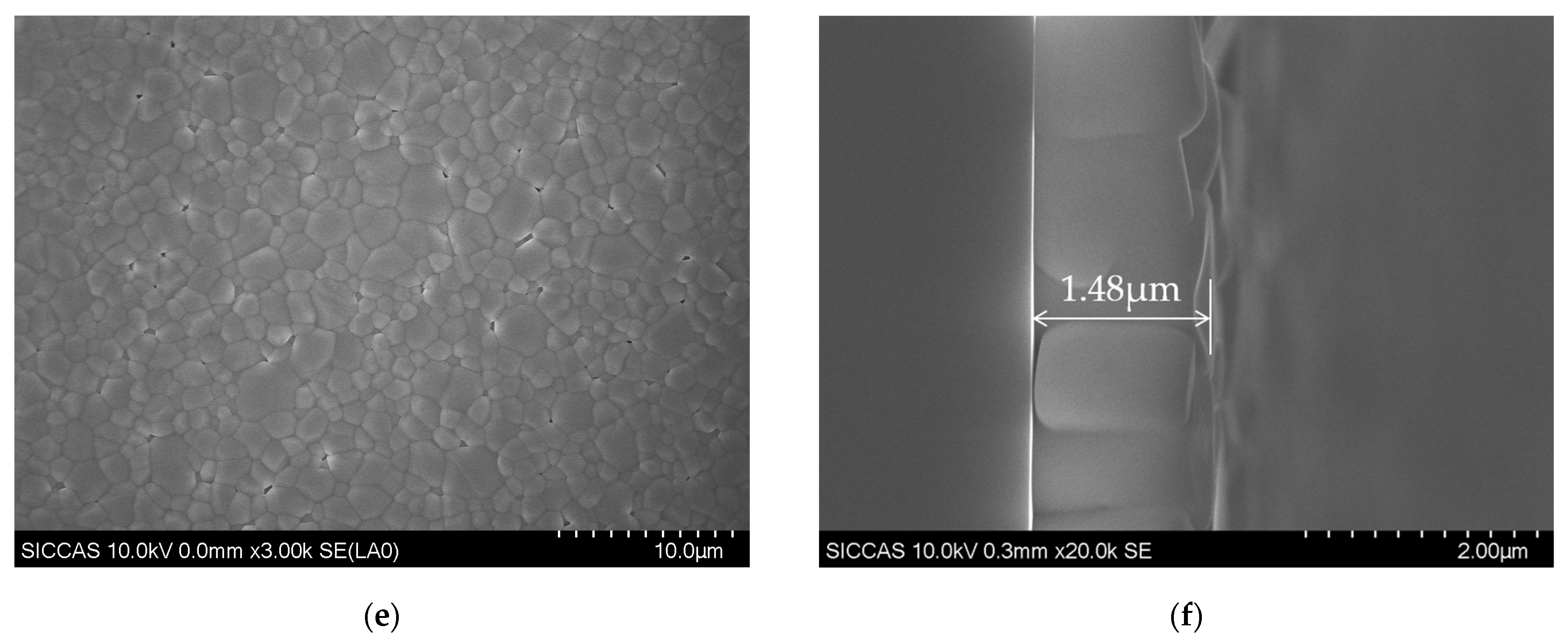
3.1. Structural Properties
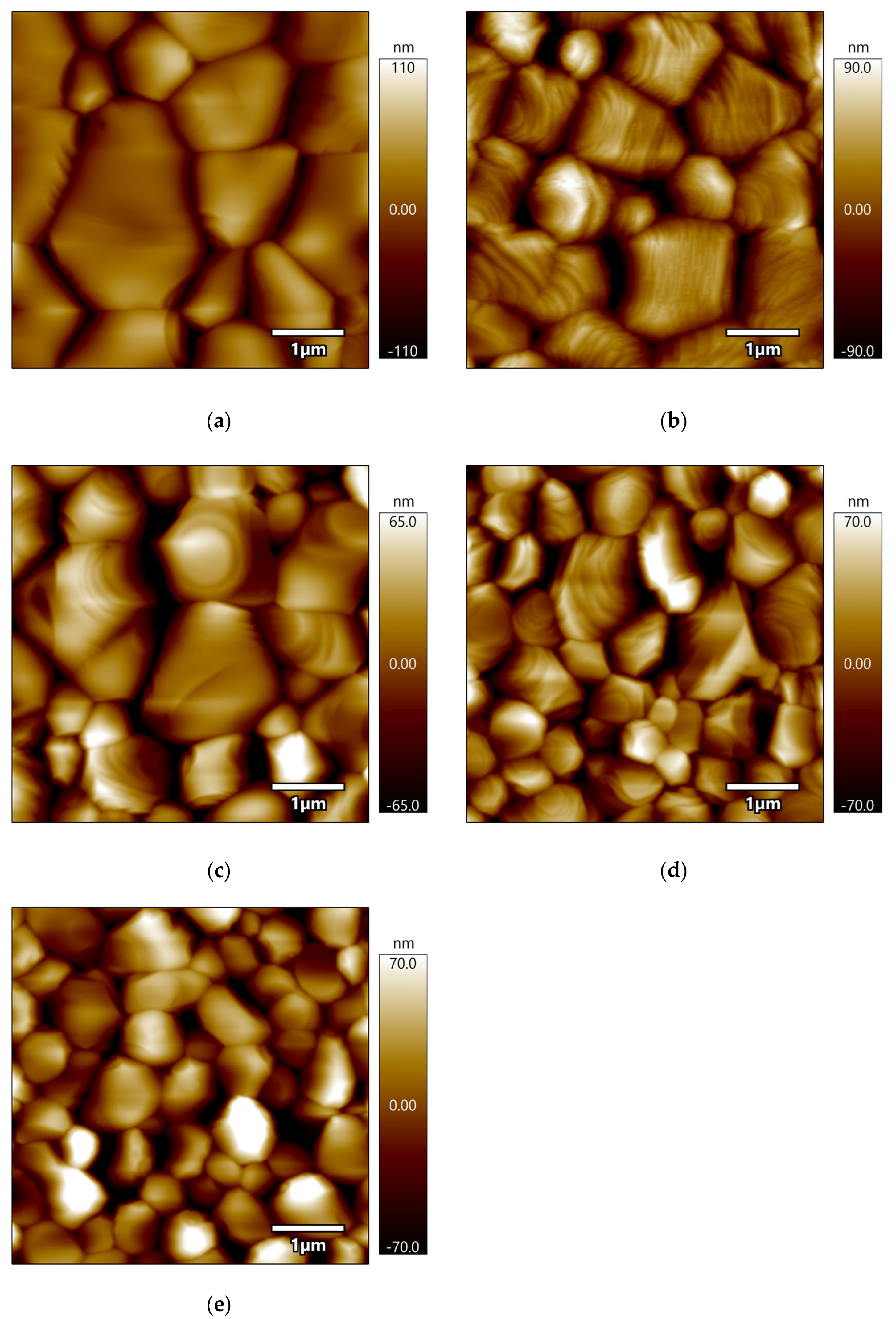
3.2. Morphological Properties
3.3. Optical Properties
4. Conclusions
Author Contributions
Funding
Institutional Review Board Statement
Informed Consent Statement
Data Availability Statement
Conflicts of Interest
References
- Kruschwitz, J.D.T.; Pawlewicz, W.T. Optical and Durability Properties of Infrared Transmitting Thin Films. Appl. Optics 1997, 36, 2157–2159. [Google Scholar] [CrossRef]
- Raut, H.K.; Ganesh, V.A.; Nair, A.S.; Ramakrishna, S. Anti-Reflective Coatings: A Critical, in-Depth Review. Energy Environ. Sci. 2011, 4, 3779–3804. [Google Scholar] [CrossRef]
- Yamauchi, M.; Maruyama, S.; Ohashi, N.; Toyabe, K.; Matsumoto, Y. Epitaxial Growth of Atomically Flat KBr(111) Films via a Thin Film Ionic Liquid in a Vacuum. CrystEngComm 2016, 18, 3399–3403. [Google Scholar] [CrossRef]
- Kolodziej, J.J.; Such, B.; Czuba, P.; Krok, F.; Piatkowski, P.; Szymonski, M. Scanning-Tunneling/Atomic-Force Microscopy Study of the Growth of KBr Films on InSb(001). Surf. Sci. 2002, 506, 12–22. [Google Scholar] [CrossRef]
- Saiki, K.; Nakamura, Y.; Nishida, N.; Gao, W.; Koma, A. Heteroepitaxy of Alkali Halide on Si and GaAs Substrates. Surf. Sci. 1994, 301, 29–38. [Google Scholar] [CrossRef]
- Rahmlow, T.D., Jr.; Lazo-Wasem, J.E.; Rahmlow, D.A. Characterization of Far-Infrared Optical Thin Film Materials and Blends: AgBr, AgCl, KBr, Csl, and CsBr. In Optical Diagnostic Methods for Inorganic Transmissive Materials; Datla, R.V., Hanssen, L.M., Eds.; SPIE: San Diego, CA, USA, 1998; pp. 73–84. [Google Scholar]
- Rai, R.; Yadav, R.P.; Pandit, T.; Jammal, N.; Singh, A.K.; Singh, B.K. Morphological Evaluation of Self-Affine Thermally Grown KBr Thin Films. Mater. Res. Express 2019, 6, 126422. [Google Scholar] [CrossRef]
- Johnson, K.W.; Bell, E.E. Far-Infrared Optical Properties of KCl and KBr. Phys. Rev. 1969, 187, 1044–1052. [Google Scholar] [CrossRef]
- Hadni, A.; Claudel, J.; Chanal, D.; Strimer, P.; Vergnat, P. Optical Constants of Potassium Bromide in the Far Infrared. Phys. Rev. 1967, 163, 836–843. [Google Scholar] [CrossRef]
- Rai, R.; Triloki; Singh, B.K.; Jammal, N.F.A. Correlation between Photoemissive and Morphological Properties of KBr Thin Film Photocathodes. Nucl. Instrum. Methods Phys. Res. Sect. A Accel. Spectrometers Detect. Assoc. Equip. 2018, 912, 6–10. [Google Scholar] [CrossRef]
- Rai, R.; Singh, B.K. Study of KBr Thin FIlms for EUV and FUV Sensitive Photocathode Devices. In Proceedings of the 60th DAE-BRNS Symposium on Nuclear Physics, Prasanthi Nilayam, India, 7–11 December 2015. [Google Scholar]
- Rai, R.; Triloki, T.; Singh, B.K. X-Ray Diffraction Line Profile Analysis of KBr Thin Films. Appl. Phys. A 2016, 122, 774. [Google Scholar] [CrossRef]
- Alidjanov, E.K.; Atabaev, B.G.; Gaipov, S.; Boltaev, N.N. Target Current Spectroscopy of the Alkali Halides KC1, CsC1 and KBr. Thin Solid Film. 1994, 250, 268–272. [Google Scholar] [CrossRef]
- He, W.; Vilayurganapathy, S.; Joly, A.G.; Droubay, T.C.; Chambers, S.A.; Maldonado, J.R.; Hess, W.P. Comparison of CsBr and KBr Covered Cu Photocathodes: Effects of Laser Irradiation and Work Function Changes. Appl. Phys. Lett. 2013, 102, 071604. [Google Scholar] [CrossRef]
- Tremsin, A.S.; Siegmund, O.H.W. Heat Enhancement of Radiation Resistivity of Evaporated CsI, KI and KBr Photocathodes. Nucl. Instrum. Methods Phys. Res. Sect. A Accel. Spectrometers Detect. Assoc. Equip. 2000, 442, 337–341. [Google Scholar] [CrossRef]
- Larruquert, J.I.; Méndez, J.A.; Aznárez, J.A.; Tremsin, A.S.; Siegmund, O.H.W. Optical Properties and Quantum Efficiency of Thin-Film Alkali Halides in the Far Ultraviolet. Appl. Opt. 2002, 41, 2532. [Google Scholar] [CrossRef]
- Shao, J.; Dobrowolski, J.A. Multilayer Interference Filters for the Far-Infrared and Submillimeter Regions. Appl. Opt. 1993, 32, 2361. [Google Scholar] [CrossRef] [PubMed]
- Tremsin, A.S.; Siegmund, O.H.W. UV Radiation Resistance and Solar Blindness of CsI and KBr Photocathodes. IEEE Trans. Nucl. Sci. 2001, 48, 421–425. [Google Scholar] [CrossRef]
- Wang, Y.; Tang, W.; Zhang, L. Crystalline Size Effects on Texture Coefficient, Electrical and Optical Properties of Sputter-Deposited Ga-Doped ZnO Thin Films. J. Mater. Sci. Technol. 2015, 31, 175–181. [Google Scholar] [CrossRef]
- Bragg, W.L. The Diffraction of Short Electromagnetic Waves by a Crystal. Scientia 1929, 23, 153. [Google Scholar]
- Choudhury, N.; Sarma, B.K. Structural Characterization of Lead Sulfide Thin Films by Means of X-Ray Line Profile Analysis. Bull. Mater. Sci. 2009, 32, 43–47. [Google Scholar] [CrossRef]
- Patterson, A.L. The Scherrer Formula for X-Ray Particle Size Determination. Phys. Rev. 1939, 56, 978–982. [Google Scholar] [CrossRef]
- Patel, V.A.; Patel, B.H. Influence of Substrate Temperature on Structure, Stoichiometry, and Energy Band Gap of Zn1−xMgxO Thin Films Deposited by Pulsed Laser Deposition. Appl. Phys. A 2022, 128, 1117. [Google Scholar] [CrossRef]
- Jaber, A.Y.; Alamri, S.N.; Aida, M.S.; Benghanem, M.; Abdelaziz, A.A. Influence of Substrate Temperature on Thermally Evaporated CdS Thin Films Properties. J. Alloys Compd. 2012, 529, 63–68. [Google Scholar] [CrossRef]
- Basak, A. Impact of Substrate Temperature on the Structural, Optical and Electrical Properties of Thermally Evaporated SnS Thin Films. Mater. Sci. Semicond. Process. 2016, 56, 381–385. [Google Scholar] [CrossRef]
- Hwang, Y.; Park, S.; Kang, M.; Um, Y. Effects of Temperature-Induced Stress on the Structural, Electrical, and Optical Properties of ZnO:Ga Thin Films Grown on Si Substrates. Current Appl. Phys. 2014, 14, S23–S28. [Google Scholar] [CrossRef]
- Hsu, J.-C.; Ma, Y.-S. Luminescence of CsI and CsI:Na Films under LED and X-Ray Excitation. Coatings 2019, 9, 751. [Google Scholar] [CrossRef]
- Kate, R.S.; Pathan, H.M.; Kalubarme, R.; Kale, B.B.; Deokate, R.J. Spray Pyrolysis: Approaches for Nanostructured Metal Oxide Films in Energy Storage Application. J. Energy Storage 2022, 54, 105387. [Google Scholar] [CrossRef]
- Heavens, O.S. Handbook of Optical Constants of Solids II. J. Mod. Opt. 1992, 39, 189. [Google Scholar] [CrossRef]
- Hidaka, T.; Morikawa, T.; Shimada, J. Spectroscopic Small Loss Measurements on Infrared Transparent Materials. Appl. Opt. 1980, 19, 3763. [Google Scholar] [CrossRef] [PubMed]


| Substrate Temperature (°C) | 50 | 100 | 150 | 200 | 250 |
| RMS Roughness (nm) | 25.13 | 26.56 | 24.64 | 25.16 | 28.30 |
Disclaimer/Publisher’s Note: The statements, opinions and data contained in all publications are solely those of the individual author(s) and contributor(s) and not of MDPI and/or the editor(s). MDPI and/or the editor(s) disclaim responsibility for any injury to people or property resulting from any ideas, methods, instructions or products referred to in the content. |
© 2025 by the authors. Licensee MDPI, Basel, Switzerland. This article is an open access article distributed under the terms and conditions of the Creative Commons Attribution (CC BY) license (https://creativecommons.org/licenses/by/4.0/).
Share and Cite
Xu, T.; Cai, Q.; Duan, W.; Wang, K.; Jia, B.; Luo, H.; Liu, D. Effect of Substrate Temperature on the Structural, Morphological, and Infrared Optical Properties of KBr Thin Films. Materials 2025, 18, 3644. https://doi.org/10.3390/ma18153644
Xu T, Cai Q, Duan W, Wang K, Jia B, Luo H, Liu D. Effect of Substrate Temperature on the Structural, Morphological, and Infrared Optical Properties of KBr Thin Films. Materials. 2025; 18(15):3644. https://doi.org/10.3390/ma18153644
Chicago/Turabian StyleXu, Teng, Qingyuan Cai, Weibo Duan, Kaixuan Wang, Bojie Jia, Haihan Luo, and Dingquan Liu. 2025. "Effect of Substrate Temperature on the Structural, Morphological, and Infrared Optical Properties of KBr Thin Films" Materials 18, no. 15: 3644. https://doi.org/10.3390/ma18153644
APA StyleXu, T., Cai, Q., Duan, W., Wang, K., Jia, B., Luo, H., & Liu, D. (2025). Effect of Substrate Temperature on the Structural, Morphological, and Infrared Optical Properties of KBr Thin Films. Materials, 18(15), 3644. https://doi.org/10.3390/ma18153644