
Amorphous SiC Thin Films Deposited by Plasma-Enhanced Chemical Vapor Deposition for Passivation in Biomedical Devices


Abstract
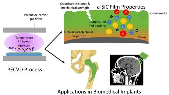
1. Introduction
2. Deposition of a-SiC Films
2.1. Sputtering Method Employed for a-SiC Film Deposition
2.2. PECVD Method Employed for a-SiC Film Deposition
2.3. Optimal Deposition Technique for Biomedical Applications
3. Controlling a-SiC Film Properties for PECVD
3.1. Stoichiometry of a-SiC Films
3.1.1. Variation of Stoichiometry with Precursor Gas Ratio
3.1.2. Variation of Stoichiometry with RF Power
3.1.3. Variation of Stoichiometry with Deposition Temperature
3.1.4. Presence of Hydrogen in a-SiC
3.1.5. Presence of Oxygen in a-SiC
3.1.6. Stoichiometry of a-SiC Films for Biomedical Applications
3.2. Resistivity of a-SiC Films
3.2.1. Variation of Resistivity with Stoichiometry
3.2.2. Variation of Resistivity with Deposition Temperature
3.2.3. Varying a-SiC Resistivity by Doping and/or Post-Deposition Annealing
3.2.4. Resistivity of a-SiC Films for Biomedical Applications
3.3. Optoelectronic Properties of a-SiC Films
3.3.1. Optical Bandgap
3.3.2. Refractive Index
3.3.3. Optical Properties of a-SiC Films for Biomedical Applications
3.4. Stress in a-SiC Films
3.4.1. Variation of Stress with Film Composition
3.4.2. Variation of Stress with RF Power
3.4.3. Variation of Stress with Deposition Pressure
3.4.4. Variation of Stress with Deposition Temperature
3.4.5. Modifying Film Stress with Post-Deposition Annealing
3.4.6. Evolution of Film Stress over Time
3.4.7. Stress in a-SiC Films for Biomedical Applications
3.5. Mechanical Properties of a-SiC Films
3.5.1. Variation of Film Mechanical Properties with Stoichiometry
3.5.2. Variation of Mechanical Properties with Deposition Temperature
3.5.3. Variation of Mechanical Properties with Post-Deposition Annealing
3.5.4. Mechanical Properties of a-SiC Films for Biomedical Applications
3.6. Passivation Properties
3.6.1. Dissolution Rate in Chemical Solutions
3.6.2. Conformal Coating and Uniformity
3.6.3. Surface Roughness
4. Perspectives
5. Conclusions
Author Contributions
Funding
Data Availability Statement
Conflicts of Interest
References
- Wijesundara, M.B.J.; Azevedo, R. Silicon Carbide Microsystems for Harsh Environments; MEMS Reference Shelf; Springer: New York, NY, USA, 2011; Volume 22. [Google Scholar] [CrossRef]
- Ivashchenko, V.I.; Porada, O.K.; Ivashchenko, L.A.; Rusakov, G.V.; Dub, S.M.; Popov, V.M. Hydrogenated Amorphous Silicon Carbide Films as Perspective Tribological Coatings and Semiconductor Layers. In Hydrogen Materials Science and Chemistry of Carbon Nanomaterials; Veziroglu, T.N., Zaginaichenko, Y.S., Schur, D.V., Baranowski, B., Shpak, A.P., Skorokhod, V.V., Eds.; NATO Science Series II: Mathematics, Physics and Chemistry; Springer: Dordrecht, The Netherlands, 2004; Volume 172, pp. 339–346. [Google Scholar] [CrossRef]
- Porada, O.K.; Ivashchenko, V.I.; Ivashchenko, L.A.; Rusakov, G.V.; Dub, S.N.; Stegnij, A.I. a-SiC:H films as perspective wear-resistant coatings. Surf. Coat. Technol. 2004, 180–181, 122–126. [Google Scholar] [CrossRef]
- Barbouche, M.; Benabderrahmane Zaghouani, R.; Ben Ammar, N.E.; Aglieri, V.; Nasser, H.; Turan, R.; Ezzaouia, H. Effect of amorphous SiC layer on electrical and optical properties of Al/a-SiC/c-Si Schottky diode for optoelectronic applications. J. Mater. Sci. Mater. Electron. 2021, 32, 20598–20611. [Google Scholar] [CrossRef]
- Cocorullo, G.; Terzini, E.; della Corte, F.G.; de Rosa, R.; Rendina, I.; Rubino, A. a-Si:Hra-SiC:H waveguides and modulators for low-cost silicon-integrated optoelectronics. J. Non-Cryst. Solids 1998, 227–230, 1118–1122. [Google Scholar] [CrossRef]
- King, S.W.; Bielefeld, J.; Xu, G.; Lanford, W.A.; Matsuda, Y.; Dauskardt, R.H.; Kim, N.; Hondongwa, D.; Olasov, L.; Daly, B.; et al. Influence of network bond percolation on the thermal, mechanical, electrical and optical properties of high and low-k a-SiC:H thin films. J. Non-Cryst. Solids 2013, 379, 67–79. [Google Scholar] [CrossRef]
- Chen, J.; Calvin, J.J.; King, S.W.; Woodfield, B.F.; Navrotsky, A. Energetics of porous amorphous low-k SiOCH dielectric films. J. Chem. Thermodyn. 2019, 139, 105885. [Google Scholar] [CrossRef]
- Knaack, G.L.; McHail, D.G.; Borda, G.; Koo, B.; Peixoto, N.; Cogan, S.F.; Dumas, T.C.; Pancrazio, J.J. In vivo Characterization of Amorphous Silicon Carbide As a Biomaterial for Chronic Neural Interfaces. Front. Neurosci. 2016, 10, 301. [Google Scholar] [CrossRef]
- Yakimova, R.; Petoral, R.M.; Yazdi, G.R.; Vahlberg, C.; Lloyd Spetz, A.; Uvdal, K. Surface functionalization and biomedical applications based on SiC. J. Phys. Appl. Phys. 2007, 40, 6435–6442. [Google Scholar] [CrossRef]
- Saddow, S. Silicon Carbide Technology for Advanced Human Healthcare Applications. Micromachines 2022, 13, 346. [Google Scholar] [CrossRef]
- Harder, C.; Rzany, A.; Schaldach, M. Coating of Vascular Stents with Antithrombogenic Amorphous Sil. Prog. Biomed. Res. 1999, 4, 71–77. [Google Scholar]
- Gelvez- Lizarazo, O.; Reyes-Betanzo, C. Characterization of Residual Stress in a-SiC:H Deposited by RF-PECVD for Manufacturing of Membranes for Cell Culture. MRS Proc. 2016, 1812, 117–122. [Google Scholar] [CrossRef]
- Iliescu, C.; Chen, B.; Poenar, D.P.; Lee, Y.Y. PECVD amorphous silicon carbide membranes for cell culturing. Sens. Actuators B Chem. 2008, 129, 404–411. [Google Scholar] [CrossRef]
- Amon, M.; Bolz, A.; Schaldach, M. Improvement of stenting therapy with a silicon carbide coated tantalum stent. J. Mater. Sci. Mater. Med. 1996, 7, 273–278. [Google Scholar] [CrossRef]
- Fares, C.; Hsu, S.-M.; Xian, M.; Xia, X.; Ren, F.; Mecholsky, J.J.; Gonzaga, L.; Esquivel-Upshaw, J. Demonstration of a SiC Protective Coating for Titanium Implants. Materials 2020, 13, 3321. [Google Scholar] [CrossRef]
- Chen, Z.; Fares, C.; Elhassani, R.; Ren, F.; Kim, M.; Hsu, S.-M.; Clark, A.E.; Esquivel-Upshaw, J.F. Demonstration of SiO2/SiC-based protective coating for dental ceramic prostheses. J. Am. Ceram. Soc. 2019, 102, 6591–6599. [Google Scholar] [CrossRef] [PubMed]
- Hsu, S.-M.; Ren, F.; Chen, Z.; Kim, M.; Fares, C.; Clark, A.E.; Neal, D.; Esquivel-Upshaw, J.F. Novel Coating to Minimize Corrosion of Glass-Ceramics for Dental Applications. Materials 2020, 13, 1215. [Google Scholar] [CrossRef] [PubMed]
- Cogan, S.F.; Edell, D.J.; Guzelian, A.A.; Ping Liu, Y.; Edell, R. Plasma-enhanced chemical vapor deposited silicon carbide as an implantable dielectric coating. J. Biomed. Mater. Res. 2003, 67A, 856–867. [Google Scholar] [CrossRef] [PubMed]
- Hsu, J.-M.; Tathireddy, P.; Rieth, L.; Normann, A.R.; Solzbacher, F. Characterization of a-SiCx:H thin films as an encapsulation material for integrated silicon based neural interface devices. Thin Solid Film. 2007, 516, 34–41. [Google Scholar] [CrossRef] [PubMed]
- Register, J. SiC for Advanced Biological Applications. Ph.D. Dissertation, University of South Florida, Tampa, FL, USA, 2014. Available online: http://scholarcommons.usf.edu/etd/5113 (accessed on 10 January 2023).
- Schmitt, G. Passivation and corrosion of microelectrode arrays. Electrochim. Acta 1999, 44, 3865–3883. [Google Scholar] [CrossRef]
- Faßbender, F.; Schmitt, G.; Schöning, M.J.; Lüth, H.; Buß, G.; Schultze, J.-W. Optimization of passivation layers for corrosion protection of silicon-based microelectrode arrays. Sens. Actuators B Chem. 2000, 68, 128–133. [Google Scholar] [CrossRef]
- Lotti, F.; Ranieri, F.; Vadalà, G.; Zollo, L.; Di Pino, G. Invasive Intraneural Interfaces: Foreign Body Reaction Issues. Front. Neurosci. 2017, 11, 497. [Google Scholar] [CrossRef]
- Diaz-Botia, C.A.; Luna, L.E.; Neely, R.M.; Chamanzar, M.; Carraro, C.; Carmena, J.M.; Sabes, P.N.; Maboudian, R.; Maharbiz, M.M. A silicon carbide array for electrocorticography and peripheral nerve recording. J. Neural Eng. 2017, 14, 056006. [Google Scholar] [CrossRef] [PubMed]
- Sridharan, A.; Muthuswamy, J. Quantitative Assessment of the Mechanical Properties of the Neural Interface. In Handbook of Neuroengineering; Thakor, N.V., Ed.; Springer Nature: Singapore, 2023; pp. 213–259. [Google Scholar] [CrossRef]
- Szostak, K.M.; Grand, L.; Constandinou, T.G. Neural Interfaces for Intracortical Recording: Requirements, Fabrication Methods, and Characteristics. Front. Neurosci. 2017, 11, 665. [Google Scholar] [CrossRef] [PubMed]
- Axpe, E.; Orive, G.; Franze, K.; Appel, E.A. Towards brain-tissue-like biomaterials. Nat. Commun. 2020, 11, 3423. [Google Scholar] [CrossRef]
- Sharafkhani, N.; Kouzani, A.Z.; Adams, S.D.; Long, J.M.; Lissorgues, G.; Rousseau, L.; Orwa, J.O. Neural tissue-microelectrode interaction: Brain micromotion, electrical impedance, and flexible microelectrode insertion. J. Neurosci. Methods 2022, 365, 109388. [Google Scholar] [CrossRef]
- Thielen, B.; Meng, E. A comparison of insertion methods for surgical placement of penetrating neural interfaces. J. Neural Eng. 2021, 18, 041003. [Google Scholar] [CrossRef] [PubMed]
- Geramifard, N.; Dousti, B.; Nguyen, C.; Abbott, J.; Cogan, S.F.; Varner, V.D. Insertion mechanics of amorphous SiC ultra-micro scale neural probes. J. Neural Eng. 2022, 19, 026033. [Google Scholar] [CrossRef]
- Nguyen, C.K.; Abbott, J.R.; Negi, S.; Cogan, S.F. Evaluation of Amorphous Silicon Carbide on Utah Electrode Arrays by Thermal Accelerated Aging. In Proceedings of the 2021 43rd Annual International Conference of the IEEE Engineering in Medicine & Biology Society (EMBC), Virtual, 1–5 November 2021; IEEE: Piscataway, NJ, USA, 2021; pp. 6623–6626. [Google Scholar] [CrossRef]
- Fu, X.-A.; Jezeski, R.; Zorman, C.A.; Mehregany, M. Use of deposition pressure to control residual stress in polycrystalline SiC films. Appl. Phys. Lett. 2004, 84, 341–343. [Google Scholar] [CrossRef]
- Locke, C.W.; Severino, A.; La Via, F.; Reyes, M.; Register, J.; Saddow, S.E. Chapter 2—SiC Films and Coatings: Amorphous, Polycrystalline, and Single Crystal Forms. In Silicon Carbide Biotechnology; Elsevier: Amsterdam, The Netherlands, 2012; pp. 17–61. Available online: https://www.sciencedirect.com/science/article/pii/B9780123859068000027 (accessed on 10 January 2023).
- Knaack, G.L.; Charkhkar, H.; Cogan, S.F.; Pancrazio, J.J. Chapter 8—Amorphous Silicon Carbide for Neural Interface Applications. In Silicon Carbide Biotechnology, 2nd ed.; Elsevier: Amsterdam, The Netherlands, 2016; pp. 249–260. [Google Scholar]
- Prasad, A.; Xue, Q.-S.; Sankar, V.; Nishida, T.; Shaw, G.; Streit, W.J.; Sanchez, J.C. Comprehensive characterization and failure modes of tungsten microwire arrays in chronic neural implants. J. Neural Eng. 2012, 9, 056015. [Google Scholar] [CrossRef]
- El Khakani, M.A.; Chaker, M.; Jean, A.; Boily, S.; Kieffer, J.C.; O’Hern, M.E.; Ravet, M.F.; Rousseaux, F. Hardness and Young’s modulus of amorphous a -SiC thin films determined by nanoindentation and bulge tests. J. Mater. Res. 1994, 9, 96–103. [Google Scholar] [CrossRef]
- Sommakia, S.; Lee, H.C.; Gaire, J.; Otto, K.J. Materials approaches for modulating neural tissue responses to implanted microelectrodes through mechanical and biochemical means. Curr. Opin. Solid State Mater. Sci. 2014, 18, 319–328. [Google Scholar] [CrossRef]
- Feng, C.; Frewin, C.L.; Tanjil, M.R.-E.; Everly, R.; Bieber, J.; Kumar, A.; Wang, M.C.; Saddow, S.E. A Flexible a-SiC-Based Neural Interface Utilizing Pyrolyzed-Photoresist Film (C) Active Sites. Micromachines 2021, 12, 821. [Google Scholar] [CrossRef]
- Deku, F.; Cohen, Y.; Joshi-Imre, A.; Kanneganti, A.; Gardner, T.J.; Cogan, S.F. Amorphous silicon carbide ultramicroelectrode arrays for neural stimulation and recording. J. Neural Eng. 2018, 15, 016007. [Google Scholar] [CrossRef]
- Rzany, A.; Schaldach, M. Smart Material Silicon Carbide: Reduced Activation of Cells and Proteins on a-SiC:H-coated Stainless Steel. Prog. Biomed. Res. 2001, 6, 182–194. [Google Scholar]
- Frewin, C.L. The Neuron-Silicon Carbide Interface: Biocompatibility Study and BMI Device Development. Ph.D. Dissertation, University of South Florida, Tampa, FL, USA, 2009. Available online: https://digitalcommons.usf.edu/etd/1973/ (accessed on 10 January 2023).
- Knaack, G.L. In Vitro and In Vivo Biocompatibility Testing of Silicon Carbide for Neural Interfaces. Ph.D. Dissertation, George Mason University, Fairfax, VA, USA, 2011. Available online: https://mars.gmu.edu/server/api/core/bitstreams/489502f5-0c11-45b9-823b-b1520ab8036f/content (accessed on 10 January 2023).
- Rizal, U.; Swain, B.S.; Rameshbabu, N.; Swain, B.P. Biocompatibility of Hydrogen-Diluted Amorphous Silicon Carbide Thin Films for Artificial Heart Valve Coating. J. Mater. Eng. Perform. 2018, 27, 2679–2686. [Google Scholar] [CrossRef]
- Nezafati, M. Biomaterial Testing Methodology for Long-Term in vivo Applications: Silicon Carbide Corrosion Resistance, Biocompatibility and Hemocompatibility. Ph.D. Dissertation, University of South Florida, Tampa, FL, USA, 2014. Available online: https://digitalcommons.usf.edu/cgi/viewcontent.cgi?article=6479&context=etd (accessed on 10 January 2023).
- Oliveros, A.; Guiseppi-Elie, A.; Saddow, S.E. Silicon carbide: A versatile material for biosensor applications. Biomed. Microdevices 2013, 15, 353–368. [Google Scholar] [CrossRef] [PubMed]
- Beygi, M.; Bentley, J.T.; Frewin, C.L.; Kuliasha, C.A.; Takshi, A.; Bernardin, E.K.; La Via, F.; Saddow, S.E. Fabrication of a Monolithic Implantable Neural Interface from Cubic Silicon Carbide. Micromachines 2019, 10, 430. [Google Scholar] [CrossRef]
- Frewin, C.; Beygi, M.; Bernardin, E.; Feng, C.Y.; La Via, F.; Dominguez-Viqueria, W.; Saddow, S.E. The Development of Monolithic Silicon Carbide Intracortical Neural Interfaces for Long-Term Human Implantation. Mater. Sci. Forum 2022, 1062, 195–203. [Google Scholar] [CrossRef]
- Jeakle, E.N.; Abbott, J.R.; Usoro, J.O.; Wu, Y.; Haghighi, P.; Radhakrishna, R.; Sturgill, B.S.; Nakajima, S.; Thai, T.T.D.; Pancrazio, J.J.; et al. Chronic Stability of Local Field Potentials Using Amorphous Silicon Carbide Microelectrode Arrays Implanted in the Rat Motor Cortex. Micromachines 2023, 14, 680. [Google Scholar] [CrossRef] [PubMed]
- Bullot, J.; Schmidt, M.P. Physics of Amorphous Silicon–Carbon Alloys. Phys. Status Solidi B 1987, 143, 345–418. [Google Scholar] [CrossRef]
- Choi, W.K.; Lee, L.P.; Foo, S.L.; Gangadharan, S.; Chong, N.B.; Tan, L.S. Oxidation study of plasma-enhanced chemical vapor deposited and rf sputtered hydrogenated amorphous silicon carbide films. J. Appl. Phys. 2001, 89, 1942. [Google Scholar] [CrossRef]
- Fraga, M.; Pessoa, R. Progresses in Synthesis and Application of SiC Films: From CVD to ALD and from MEMS to NEMS. Micromachines 2020, 11, 799. [Google Scholar] [CrossRef]
- Mahmoodi, M.; Ghazanfari, L. Fundamentals of Biomedical Applications of Biomorphic SiC. In Properties and Applications of Silicon Carbide; Gerhardt, R., Ed.; InTech: Horwich, UK, 2011. [Google Scholar] [CrossRef]
- Kaloyeros, A.E.; Arkles, B. Silicon Carbide Thin Film Technologies: Recent Advances in Processing, Properties, and Applications—Part I Thermal and Plasma CVD. ECS J. Solid State Sci. Technol. 2023, 12, 103001. [Google Scholar] [CrossRef]
- Herrera-Celis, J.; Reyes-Betanzo, C.; Gelvez-Lizarazo, O.; Arriaga, L.G.; Itzmoyotl-Toxqui, A. Low residual stress in hydrogenated amorphous silicon-carbon films deposited by low-temperature PECVD. J. Mater. Res. Technol. 2019, 8, 5581–5590. [Google Scholar] [CrossRef]
- Daves, W.; Krauss, A.; Behnel, N.; Häublein, V.; Bauer, A.; Frey, L. Amorphous silicon carbide thin films (a-SiC:H) deposited by plasma-enhanced chemical vapor deposition as protective coatings for harsh environment applications. Thin Solid Film. 2011, 519, 5892–5898. [Google Scholar] [CrossRef]
- King, S.W.; Ross, L.; Li, H.; Xu, G.; Bielefeld, J.; Atkins, R.E.; Henneghan, P.D.; Davis, K.; Johnson, D.C.; Lanford, W.A. Influence of hydrogen content and network connectivity on the coefficient of thermal expansion and thermal stability for a-SiC:H thin films. J. Non-Cryst. Solids 2014, 389, 78–85. [Google Scholar] [CrossRef]
- Honda, K.; Matsumoto, A.; Kondo, B.; Shimizu, Y. High-performance carbon-rich amorphous silicon–carbon alloy semiconductors with low optical gaps. Phys. E Low-Dimens. Syst. Nanostruct. 2023, 148, 115652. [Google Scholar] [CrossRef]
- Donercark, E.; Sedani, S.H.; Kabaçelik, I.; Salimi, A.; Turan, R. Interface and material properties of wide band gap a-SiCx:H thin films for solar cell applications. Renew. Energy 2022, 183, 781–790. [Google Scholar] [CrossRef]
- Amorim, M.; Savio, R.; Massi, M.; Santiago, H. Applications of SiC-Based Thin Films in Electronic and MEMS Devices. In Physics and Technology of Silicon Carbide Devices; Hijikata, Y., Ed.; InTech: Horwich, UK, 2012. [Google Scholar] [CrossRef]
- Diaz-Botia, C.A. Silicon Carbide Technologies for Interfacing with the Nervous System. Ph.D. Dissertation, University of California, Berkeley, CA, USA, 2017. Available online: https://escholarship.org/uc/item/35w3d01b (accessed on 10 January 2023).
- Matsunami, H.; Masahiro, H.; Tanaka, T. Structures and physical properties of sputtered amorphous SiC films. J. Electron. Mater. 1979, 8, 249–260. [Google Scholar] [CrossRef]
- Choi, W.K.; Loo, F.L.; Ling, C.H.; Loh, F.C.; Tan, K.L. Structural and electrical studies of radio frequency sputtered hydrogenated amorphous silicon carbide films. J. Appl. Phys. 1995, 78, 7289–7294. [Google Scholar] [CrossRef]
- Choi, W.K.; Loo, F.L.; Loh, F.C.; Tan, K.L. Effects of hydrogen and rf power on the structural and electrical properties of rf sputtered hydrogenated amorphous silicon carbide films. J. Appl. Phys. 1996, 80, 1611–1616. [Google Scholar] [CrossRef]
- Ledermann, N.; Baborowski, J.; Muralt, P.; Xantopoulos, N.; Tellenbach, J.-M. Sputtered silicon carbide thin films as protective coating for MEMS applications. Surf. Coat. Technol. 2000, 125, 246–250. [Google Scholar] [CrossRef]
- Favaro, G.; Amato, A.; Arciprete, F.; Bazzan, M.; Cesarini, E.; De Matteis, F.; Dao, T.H.; Granata, M.; Honrado-Benítez, C.; Gutiérrez-Luna, N.; et al. Measurement and simulation of mechanical and optical properties of sputtered amorphous SiC coatings. arXiv 2022, arXiv:2202.04458. Available online: http://arxiv.org/abs/2202.04458 (accessed on 22 August 2023). [CrossRef]
- Lopez-Rodriguez, B.; Van Der Kolk, R.; Aggarwal, S.; Sharma, N.; Li, Z.; Van Der Plaats, D.; Scholte, T.; Chang, J.; Pereira, S.F.; Groeblacher, S.; et al. High-quality amorphous Silicon Carbide for hybrid photonic integration at low temperature. arXiv 2023, arXiv:2306.04491. Available online: http://arxiv.org/abs/2306.04491 (accessed on 3 February 2024). [CrossRef]
- Frischmuth, T.; Schneider, M.; Maurer, D.; Grille, T.; Schmid, U. Inductively-coupled plasma-enhanced chemical vapour deposition of hydrogenated amorphous silicon carbide thin films for MEMS. Sens. Actuators Phys. 2016, 247, 647–655. [Google Scholar] [CrossRef]
- Sterling, H.F.; Swann, R.C.G. Chemical vapour deposition promoted by r.f. discharge. Solid-State Electron. 1965, 8, 653–654. [Google Scholar] [CrossRef]
- El Khakani, M.A.; Chaker, M.; Jean, A.; Boily, S.; Pépin, H.; Kieffer, J.C.; Gujrathi, S.C. Effect of rapid thermal annealing on both the stress and the bonding states of a -SiC:H films. J. Appl. Phys. 1993, 74, 2834–2840. [Google Scholar] [CrossRef]
- Lee, W. X-ray photoelectron spectroscopy and Auger electron spectroscopy studies of glow discharge Si1−xCx:H films. J. Appl. Phys. 1980, 51, 3365–3372. [Google Scholar] [CrossRef]
- Fujimoto, F.; Ootuka, A.; Komaki, K.; Iwata, Y.; Yamane, I.; Yamashita, H.; Hashimoto, Y.; Tawada, Y.; Nishimura, K.; Okamoto, H.; et al. Hydrogen Content in a-SiC:H Films Prepared by Plasma Decomposition of Silane and Methane or Ethylene. Jpn. J. Appl. Phys. 1984, 23, 810. [Google Scholar] [CrossRef]
- Myong, S.Y.; Lee, H.K.; Yoon, E.; Lim, K.S. High quality microcrystalline silicon-carbide films prepared by photo-CVD method using ethylene gas as a carbon source. MRS Online Proceeding Libr. OPL 1999, 557, 603. [Google Scholar] [CrossRef]
- Ivashchenko, V.I.; Dub, S.N.; Porada, O.K.; Ivashchenko, L.A.; Skrynskyy, P.L.; Stegniy, A.I. Mechanical properties of PECVD a-SiC:H thin films prepared from methyltrichlorosilane. Surf. Coat. Technol. 2006, 200, 6533–6537. [Google Scholar] [CrossRef]
- Janz, S.; Reber, S.; Glunz, S.W. Amorphous SiC: Applications for Silicon Solar Cells. In Proceedings of the 21st European Photovoltaic Solar Energy Conference, Dresden, Germany, 4–8 September 2006; pp. 660–663. [Google Scholar]
- Joshi-Imre, A.; Black, B.J.; Abbott, J.; Kanneganti, A.; Rihani, R.; Chakraborty, B.; Danda, V.R.; Maeng, J.; Sharma, R.; Rieth, L.; et al. Chronic recording and electrochemical performance of amorphous silicon carbide-coated Utah electrode arrays implanted in rat motor cortex. J. Neural Eng. 2019, 16, 046006. [Google Scholar] [CrossRef] [PubMed]
- Desalvo, A.; Giorgis, F.; Pirri, C.F.; Tresso, E.; Rava, P.; Galloni, R.; Rizzoli, R.; Summonte, C. Optoelectronic properties, structure and composition of a-SiC:H films grown in undiluted and H2 diluted silane-methane plasma. J. Appl. Phys. 1997, 81, 7973–7980. [Google Scholar] [CrossRef]
- Vasin, A.V.; Muto, S.; Ishikawa, Y.; Rusavsky, A.V.; Kimura, T.; Lysenko, V.S.; Nazarov, A.N. Comparative study of annealing and oxidation effects in a-SiC:H and a-SiC thin films deposited by radio-frequency magnetron sputtering. Thin Solid Film. 2011, 519, 2218–2224. [Google Scholar] [CrossRef]
- Thakur, S.; Dionne, C.J.; Karna, P.; King, S.W.; Lanford, W.; Li, H.; Banerjee, S.; Merrill, D.; Hopkins, P.E.; Giri, A. Density and atomic coordination dictate vibrational characteristics and thermal conductivity of amorphous silicon carbide. Phys. Rev. Mater. 2022, 6, 094601. [Google Scholar] [CrossRef]
- Janz, S. Amorphous Silicon Carbide for Photovoltaic Applications. Ph.D. Dissertation, Fraunhofer Institute for Solar Energy Systems, Freiburg im Breisgau, Germany, 2006. [Google Scholar]
- Pham, H.T.M. PECVD Silicon Carbide—A Structural Material for Surface Micromachined Devices. Ph.D. Dissertation, TU Delft, Delft, The Netherlands, 2004. [Google Scholar]
- Guruvenket, S.; Azzi, M.; Li, D.; Szpunar, J.A.; Martinu, L.; Klemberg-Sapieha, J.E. Structural, mechanical, tribological, and corrosion properties of a-SiC:H coatings prepared by PECVD. Surf. Coat. Technol. 2010, 204, 3358–3365. [Google Scholar] [CrossRef]
- Adithi, U.; Deshpande, S.; Bhat, K.N. Material and mechanical characterization of PECVD deposited a-SiC:H with H2 dilution. In Proceedings of the 2014 IEEE 2nd International Conference on Emerging Electronics (ICEE), Bengaluru, India, 4–6 December 2014; IEEE: Bengaluru, India, 2014; pp. 1–4. [Google Scholar] [CrossRef]
- Li, D.; Guruvenket, S.; Szpunar, J.A.; Klemberg-Sapieha, J.E. Effect of C/Si Ratio on the Electrochemical Behavior of a-SiCx:H Coatings on SS301 Substrate Deposited by PECVD. Int. J. Corros. 2014, 2014, 565109. [Google Scholar] [CrossRef]
- Greenhorn, S.; Zekentes, K.; Bano, E.; Stambouli, V.; Uvarov, A. Optimizing PECVD a-SiC:H Films for Neural Interface Passivation. Key Eng. Mater. 2023, 947, 83–88. [Google Scholar] [CrossRef]
- Kwon, S.; Park, Y.; Ban, W.; Youn, C.; Lee, S.; Yang, J.; Jung, D.; Choi, T. Effect of plasma power on properties of hydrogenated amorphous silicon carbide hardmask films deposited by PECVD. Vacuum 2020, 174, 109187. [Google Scholar] [CrossRef]
- Pereyra, I.; Carreño, M.N.P.; Tabacniks, M.H.; Prado, R.J.; Fantini, M.C.A. The influence of “starving plasma” regime on carbon content and bonds in a-Si1-xCx:H thin films. J. Appl. Phys. 1998, 84, 2371–2379. [Google Scholar] [CrossRef]
- Pereyra, I.; Carrefio, M.N.P. Wide gap a-Sil_xC x:H thin films obtained under starving plasma deposition conditions. J. Non-Cryst. Solids 1996, 201, 110–118. [Google Scholar] [CrossRef]
- Solomon, I.; Schmidt, M.P.; Tran-Quoc, H. Selective low-power plasma decomposition of silane-methane mixtures for the preparation of methylated amorphous silicon. Phys. Rev. B 1988, 38, 9895–9901. [Google Scholar] [CrossRef] [PubMed]
- Deku, F.; Mohammed, S.; Joshi-Imre, A.; Maeng, J.; Danda, V.; Gardner, T.J.; Cogan, S.F. Effect of oxidation on intrinsic residual stress in amorphous silicon carbide films. J. Biomed. Mater. Res. B Appl. Biomater. 2019, 107, 1654–1661. [Google Scholar] [CrossRef]
- Yang, C.-C. Hydrogenated Amorphous Silicon Carbide Prepared using DC Saddle Field PECVD for Photovoltaic Applications. Master’s Dissertation, University of Toronto, Toronto, ON, Canada, 2011. Available online: https://tspace.library.utoronto.ca/bitstream/1807/31649/3/Yang_ChengChieh_201111_MASc_Thesis.pdf (accessed on 10 January 2023).
- Huran, J.; Hotovy, I.; Kobzev, A.P.; Balalykin, N.I. RBS study of amorphous silicon carbide films deposited by PECVD. Czechoslov. J. Phys. 2004, 54, C1006–C1010. [Google Scholar] [CrossRef]
- Demichelis, F.; Pirri, C.F.; Tresso, E.; Rigato, V.; DellaMea, G. Hydrogen diffusion and related defects in hydrogenated amorphous silicon carbide. J. Non-Cryst. Solids 1991, 128, 133–138. [Google Scholar] [CrossRef]
- Jean, A.; Chaker, M.; Diawara, Y.; Leung, P.K.; Gat, E.; Mercier, P.P.; Pépin, H.; Gujrathi, S.; Ross, G.G.; Kieffer, J.C. Characterization of a -SiC:H films produced in a standard plasma enhanced chemical vapor deposition system for x-ray mask application. J. Appl. Phys. 1992, 72, 3110–3115. [Google Scholar] [CrossRef]
- Windischmann, H.; Collins, R.W.; Cavese, J.M. Effect of Hydrogen on The Intrinsic Stress in Ion Beam Sputtered Amorphous Silicon Films. J. Non-Cryst. Solids 1986, 85, 261–272. [Google Scholar] [CrossRef]
- Demichelis, F.; Pirri, C.F.; Tresso, E. Influence of doping on the structural and optoelectronic properties of amorphous and microcrystalline silicon carbide. J. Appl. Phys. 1992, 72, 1327–1333. [Google Scholar] [CrossRef]
- Flannery, A.F.; Mourlas, N.J.; Storment, C.W.; Tsai, S.; Tan, S.H.; Heck, J.; Monk, D.; Kim, T.; Gogoi, B.; Kovacs, G.T.A. PECVD silicon carbide as a chemically resistant material for micromachined transducers. Sens. Actuators Phys. 1998, 70, 48–55. [Google Scholar] [CrossRef]
- Demichelis, F.; Pirri, C.F.; Tresso, E.; Stapinski, T. Differences in physical properties of hydrogenated and fluorinated amorphous silicon carbide prepared by reactive sputtering. J. Appl. Phys. 1992, 71, 5641–5645. [Google Scholar] [CrossRef]
- Li, X.; Wong, T.K.S.; Rusli; Yang, D. Structural and electronic properties of low dielectric constant carbon rich amorphous silicon carbide. Diam. Relat. Mater. 2003, 12, 963–967. [Google Scholar] [CrossRef]
- Arce, R.; Koropecki, R.R.; Buitrago, R.H.; Alvarez, F.; Chambouleyron, I. Direct evidence of porosity in carbon-rich hydrogenated amorphous silicon carbide films. J. Appl. Phys. 1989, 66, 4544–4546. [Google Scholar] [CrossRef][Green Version]
- Tomastik, J.; Ctvrtlik, R.; Ingr, T.; Manak, J.; Opletalova, A. Effect of Nitrogen Doping and Temperature on Mechanical Durability of Silicon Carbide Thin Films. Sci. Rep. 2018, 8, 10428. [Google Scholar] [CrossRef] [PubMed]
- Vetter, M.; Voz, C.; Ferre, R.; Martín, I.; Orpella, A.; Puigdollers, J.; Andreu, J.; Alcubilla, R. Electronic properties of intrinsic and doped amorphous silicon carbide films. Thin Solid Film. 2006, 511–512, 290–294. [Google Scholar] [CrossRef]
- Loulou, M.; Gharbi, R.; Fathallah, M.A.; Ambrosone, G.; Coscia, U.; Abbate, G.; Marino, A.; Ferrero, S.; Tresso, E. Structural, optical and electrical properties of helium diluted a-Si1−xCx:H films deposited by PECVD. J. Non-Cryst. Solids 2006, 352, 1388–1391. [Google Scholar] [CrossRef]
- Huran, J.; Hotovỳ, I.; Kobzev, A.P.; Balalykin, N.I. Influence of nitrogen concentration on conductivity of N-doped a-SiC:H films deposited by PECVD. Vacuum 2002, 67, 567–570. [Google Scholar] [CrossRef]
- Geramifard, N.; Joshi-Imre, A.; Cogan, S.F. Electrical Characterizations of Amorphous Silicon Carbide. ECS Meet. Abstr. 2019, MA2019-01, 2160. [Google Scholar] [CrossRef]
- Carreño, M.N.P.; Pereyra, I.; Fantini, M.C.A.; Takahashi, H.; Landers, R. Microvoids in diamond-like amorphous silicon carbide. J. Appl. Phys. 1994, 75, 538–542. [Google Scholar] [CrossRef][Green Version]
- Leitl, B.; Schmidt, G.; Pobegen, G.; Knoll, P.; Krenn, H. Conduction mechanisms in hydrogenated amorphous silicon carbide. J. Non-Cryst. Solids 2020, 528, 119750. [Google Scholar] [CrossRef]
- Sel, K.; Akaoğlu, B.; Atilgan, İ.; Katircioğlu, B. Effects of tail states on the conduction mechanisms in silicon carbide thin films with high carbon content. Solid-State Electron. 2011, 57, 1–8. [Google Scholar] [CrossRef]
- Le Comber, P.G. Electrical conduction in amorphous semiconductors. Sci. Prog. 1979, 66, 105–118. [Google Scholar]
- Ozdemir, O.; Atilgan, I.; Akaoglu, B.; Sel, K.; Katircioglu, B. Frequency dependence of conductivity in intrinsic amorphous silicon carbide film, assessed through admittance measurement of metal insulator semiconductor structure. Thin Solid Film. 2006, 497, 149–156. [Google Scholar] [CrossRef]
- Du, P.; Song, C.; Weng, W.; Han, G.; Shen, G. Effects of carbon additions on crystallinity and resistivity in Si–C–H thin films deposited by CVDs. J. Phys. Chem. Solids 2003, 64, 777–784. [Google Scholar] [CrossRef]
- Dutta, R.; Banerjee, P.K.; Mitra, S.S. Effect of hydrogenation on the electrical conductivity of amorphous silicon carbide. Solid State Commun. 1982, 42, 219–222. [Google Scholar] [CrossRef]
- Huran, J.; Boháček, P.; Sasinková, V.; Kleinová, A.; Mikolášek, M.; Kobzev, A.P. Amorphous silicon carbide thin films doped with P or B for the photoelectrochemical water splitting devices. Curr. Appl. Phys. 2022, 34, 101–106. [Google Scholar] [CrossRef]
- Shan, D.; Sun, D.; Tang, M.; Yang, R.; Kang, G.; Tao, T.; Cao, Y. Structures, Electronic Properties and Carrier Transport Mechanisms of Si Nano-Crystalline Embedded in the Amorphous SiC Films with Various Si/C Ratios. Nanomaterials 2021, 11, 2678. [Google Scholar] [CrossRef]
- Urbach, F. The long-wavelength edge of photographic sensitivity and of the electronic absorption of solids. Phys. Rev. 1953, 92, 1324. [Google Scholar] [CrossRef]
- Demichelis, F.; Crovini, G.; Giorgis, F.; Pirri, C.F.; Tresso, E. Effect of Power Density and Molecular Dwell Time on Compositional and Optoelectronic Properties of a-SiC:H. Solid State Commun. 1996, 98, 617–622. [Google Scholar] [CrossRef]
- Mastelaro, V.; Flank, A.M.; Fantini, M.C.A.; Bittencourt, D.R.S.; Carreño, M.N.P.; Pereyra, I. On the structural properties of a -Si1−xCx:H thin films. J. Appl. Phys. 1996, 79, 1324–1329. [Google Scholar] [CrossRef]
- Honda, K.; Yoshinaga, K.; Nagata, Y. Amorphous Carbon-Based Semiconductor Capable of Controlling Its Optical Gap and Conductivity by Incorporating Silicon and Nitrogen Atoms. ECS J. Solid State Sci. Technol. 2016, 5, P590. [Google Scholar] [CrossRef]
- Iliescu, C.; Chen, B.; Wei, J.; Pang, A.J. Characterisation of silicon carbide films deposited by plasma-enhanced chemical vapour deposition. Thin Solid Film. 2008, 516, 5189–5193. [Google Scholar] [CrossRef]
- Frischmuth, T.; Schneider, M.; Maurer, D.; Grille, T.; Schmid, U. High temperature annealing effects on the chemical and mechanical properties of inductively-coupled plasma-enhanced chemical vapor deposited a-SiC:H thin films. Thin Solid Film. 2016, 611, 6–11. [Google Scholar] [CrossRef]
- Nguyen, T.-K.; Yadav, S.; Truong, T.-A.; Han, M.; Barton, M.; Leitch, M.; Guzman, P.; Dinh, T.; Ashok, A.; Vu, H.; et al. Integrated, Transparent Silicon Carbide Electronics and Sensors for Radio Frequency Biomedical Therapy. ACS Nano 2022, 16, 10890–10903. [Google Scholar] [CrossRef]
- Register, J.; Muller, A.; King, J.; Weeber, E.; Frewin, C.L.; Saddow, S.E. Silicon Carbide Waveguides for Optogenetic Neural Stimulation. MRS Online Proc. Libr. 2012, 1433, 19–24. [Google Scholar] [CrossRef]
- Iliescu, C.; Poenar, D.P. PECVD Amorphous Silicon Carbide (α-SiC) Layers for MEMS Applications. In Physics and Technology of Silicon Carbide Devices; Hijikata, Y., Ed.; InTech: Horwich, UK, 2012. [Google Scholar] [CrossRef]
- Windischmann, H. Intrinsic Stress in Sputter-Deposited Thin Films. Crit. Rev. Solid State Mater. Sci. 1992, 17, 547–596. [Google Scholar] [CrossRef]
- Guivarc’h, A.; Richard, J.; LeContellec, M.; Ligeon, E.; Fontenille, J. Hydrogen content of amorphous silicon carbide prepared by reactive sputtering: Effects on films properties. J. Appl. Phys. 1980, 51, 2167. [Google Scholar] [CrossRef]
- Jousseaume, V.; Rochat, N.; Favennec, L.; Renault, O.; Passemard, G. Mechanical stress in PECVD a-SiC:H: Aging and plasma treatments effects. Mater. Sci. Semicond. Process. 2004, 7, 301–305. [Google Scholar] [CrossRef]
- Xu, M.; Shin, D.; Sberna, P.M.; van der Kolk, R.; Cupertino, A.; Bessa, M.A.; Norte, R.A. High-Strength Amorphous Silicon Carbide for Nanomechanics. Adv. Mater. 2023, 36, 2306513. [Google Scholar] [CrossRef] [PubMed]
- Matsuda, Y.; Kim, N.; King, S.W.; Bielefeld, J.; Stebbins, J.F.; Dauskardt, R.H. Tunable Plasticity in Amorphous Silicon Carbide Films. ACS Appl. Mater. Interfaces 2013, 5, 7950–7955. [Google Scholar] [CrossRef] [PubMed]
- Bae, S.-G.; Kim, S.; Lee, J.-A.; Jeong, Y.-G.; Shin, D.-G. Improving the mechanical properties of amorphous silicon carbide fibers by forming a protective silicon dioxide layer. Ceram. Int. 2022, 48, 30745–30753. [Google Scholar] [CrossRef]
- Shoffstall, A.J.; Srinivasan, S.; Willis, M.; Stiller, A.M.; Ecker, M.; Voit, W.E.; Pancrazio, J.J.; Capadona, J.R. A Mosquito Inspired Strategy to Implant Microprobes into the Brain. Sci. Rep. 2018, 8, 122. [Google Scholar] [CrossRef] [PubMed]
- Jiang, L.; Chen, X.; Wang, X.; Xu, L.; Stubhan, F.; Merkel, K.-H. a-SiCx:H ®lms deposited by plasma-enhanced chemical vapor deposition at low temperature used for moisture and corrosion resistant applications. Thin Solid Film. 1999, 352, 97–101. [Google Scholar] [CrossRef]
- Flannery, A.F.; Mourlas, N.J.; Storment, C.W.; Tsai, S.; Tan, S.H.; Kovacs, G.T.A. PECVD silicon carbide for micromachined transducers. In Proceedings of the International Solid State Sensors and Actuators Conference (Transducers’97), Chicago, IL, USA, 6–10 June 1997; IEEE: Chicago, IL, USA, 1997; Volume 1, pp. 217–220. [Google Scholar] [CrossRef]
- Avram, M.; Avram, A.; Bragaru, A.; Chen, B.; Poenar, D.P.; Iliescu, C. Low stress PECVD amorphous silicon carbide for MEMS applications. In Proceedings of the CAS 2010 Proceedings (International Semiconductor Conference), Sinaia, Romania, 11–13 October 2010; IEEE: Sinaia, Romania, 2010; pp. 239–242. [Google Scholar] [CrossRef]
- Peri, B.; Borah, B.; Dash, R.K. Effect of RF power and gas flow ratio on the growth and morphology of the PECVD SiC thin film s for MEMS applications. Bull. Mater. Sci. 2015, 38, 1105–1112. [Google Scholar] [CrossRef]
- Awad, Y.O. Characterization of Amorphous Silicon Carbide and Silicon Carbonitride Thin Films Synthesized by Polymer-Source Chemical Vapor Deposition: Mechanical Structural and Metal-Interface Properties. Ph.D. Dissertation, University of Sherbrooke, Sherbrooke, CA, USA, 2006. Available online: https://savoirs.usherbrooke.ca/handle/11143/1821 (accessed on 12 August 2023).
- Retana-González, R.A.; Reyes-Betanzo, C.; Gómez-Montaño, F.J.; Orduña-Díaz, A. Development of a hydrogenated amorphous silicon carbide-based biosensor for E. coli detection. MRS Adv. 2023, 8, 1438–1444. [Google Scholar] [CrossRef]
- Boussaa, S.A.; Benfadel, K.; Khodja, A.T.; Ayachi, M.; Boulil, R.; Bekhedda, K.; Talbi, L.; Boukezzata, A.; Ouadah, Y.; Allam, D.; et al. Elaboration and Characterization of Amorphous Silicon Carbide Thin Films (a-SiC) by Sputerring Magnetron Technique for Photoelectrochemical CO2 Conversion. Silicon 2023, 15, 1145–1157. [Google Scholar] [CrossRef]
- Hernández-Acosta, M.A.; Martines-Arano, H.; Soto-Ruvalcaba, L.; Martínez-González, C.L.; Martínez-Gutiérrez, H.; Torres-Torres, C. Fractional thermal transport and twisted light induced by an optical two-wave mixing in single-wall carbon nanotubes. Int. J. Therm. Sci. 2020, 147, 106136. [Google Scholar] [CrossRef]
- Fabbri, L.; Bordoni, C.; Barquinha, P.; Crocco, J.; Fraboni, B.; Cramer, T. Accurate determination of band tail properties in amorphous semiconductor thin film with Kelvin probe force microscopy. APL Mater. 2023, 11, 061123. [Google Scholar] [CrossRef]
- Xie, Z.; Zhang, Y.; Huang, S.; Li, Z.; Cheng, Q.; Zhou, J. Towards quantitative determination of atomic structures of amorphous materials in three dimensions. Natl. Sci. Open 2023, 2, 20220048. [Google Scholar] [CrossRef]
- Ivashchenko, V.I.; Turchi, P.E.A.; Shevchenko, R.V.; Gorb, L.; Leszczynski, J.; Kozak, A.O. An effect of nitrogen incorporation on the structure and properties of amorphous SiC: First-principles molecular dynamics simulations. Thin Solid Film. 2022, 756, 139349. [Google Scholar] [CrossRef]
- Yan, Z.; Liu, R.; Liu, B.; Shao, Y.; Liu, M. Molecular Dynamics Simulation Studies of Properties, Preparation, and Performance of Silicon Carbide Materials: A Review. Energies 2023, 16, 1176. [Google Scholar] [CrossRef]


| Study | Daves [55] | Janz [79] | Pham [80] | Adithi [82] | Li/Guruvenket [81,83] |
|---|---|---|---|---|---|
| PECVD system | Oxford Plasmalab 100 Abingdon, UK | Roth & Rau AK400 Hohenstein-Ernstthal, Germany | Novellus Concept One San Jose, California | Oxford Plasmalab 100 Abingdon, UK | Applied Materials P5000 Santa Clara, CA, USA |
| Max Diameter (cm) | 20 | 15.6 | 50 | 20 | 20 |
| Power (W) | 200 | 150 | 100 | 40 |
Disclaimer/Publisher’s Note: The statements, opinions and data contained in all publications are solely those of the individual author(s) and contributor(s) and not of MDPI and/or the editor(s). MDPI and/or the editor(s) disclaim responsibility for any injury to people or property resulting from any ideas, methods, instructions or products referred to in the content. |
© 2024 by the authors. Licensee MDPI, Basel, Switzerland. This article is an open access article distributed under the terms and conditions of the Creative Commons Attribution (CC BY) license (https://creativecommons.org/licenses/by/4.0/).
Share and Cite
Greenhorn, S.; Bano, E.; Stambouli, V.; Zekentes, K. Amorphous SiC Thin Films Deposited by Plasma-Enhanced Chemical Vapor Deposition for Passivation in Biomedical Devices. Materials 2024, 17, 1135. https://doi.org/10.3390/ma17051135
Greenhorn S, Bano E, Stambouli V, Zekentes K. Amorphous SiC Thin Films Deposited by Plasma-Enhanced Chemical Vapor Deposition for Passivation in Biomedical Devices. Materials. 2024; 17(5):1135. https://doi.org/10.3390/ma17051135
Chicago/Turabian StyleGreenhorn, Scott, Edwige Bano, Valérie Stambouli, and Konstantinos Zekentes. 2024. "Amorphous SiC Thin Films Deposited by Plasma-Enhanced Chemical Vapor Deposition for Passivation in Biomedical Devices" Materials 17, no. 5: 1135. https://doi.org/10.3390/ma17051135
APA StyleGreenhorn, S., Bano, E., Stambouli, V., & Zekentes, K. (2024). Amorphous SiC Thin Films Deposited by Plasma-Enhanced Chemical Vapor Deposition for Passivation in Biomedical Devices. Materials, 17(5), 1135. https://doi.org/10.3390/ma17051135