
Epitaxial Growth of Ga2O3: A Review

 , , , ,


Abstract
1. Introduction

| Crystal Structure | Lattice Parameters | Space Group | Bandgap (eV) | Refractive Index (n) | Thermal Conductivity (W·cm−1·K−1) | Epitaxial Methods |
|---|---|---|---|---|---|---|
| α (Corundum) | a = b = 4.98–5.04, c = 13.43–13.62 | R-3C | 5.2–5.41 | 1.74–1.95 | - | Mist CVD, MOCVD, HVPE |
| β (Monoclinic) | a = 12.12–12.34, b = 3.03 and 3.04, c = 5.80–5.87 | C2/m | 4.5–4.9 | 1.68–1.89 | 0.27 (010), 0.11 (100) | MBE, Mist CVD, MOCVD, PLD, LPCVD, sputtering, HVPE |
| γ (Cubic defective spinel) | a = 8.24–8.30 | FD-3m | 4.5–5.0 | 2.0–2.1 | - | Mist CVD |
| Δ (Cubic bixbyite) | a = 9.4–10 | Ia-3 | 4.8–5.0 | 1.8 | - | Mist CVD |
| κ (Orthorhombic) | a = 5.0463, b = 8.7020, c = 9.2833 | Pna21 | 4.6–4.9 | - | - | MBE, Mist CVD, MOCVD, PLD, HVPE |
| Properties | Si | GaAs | 4H-SiC | GaN | Ga2O3 | Diamond |
|---|---|---|---|---|---|---|
| Bandgap, Eg (eV) | 1.1 | 1.4 | 3.3 | 3.4 | 4.85 | 5.5 |
| Breakdown field, Ec (MV·cm−1) | 0.3 | 0.4 | 2.5 | 3.3 | 8 | 10 |
| Electron mobility, μ (cm2·V−1·s−1) | 1400 | 8000 | 1000 | 1250 | 300 | 2000 |
| Relative dielectric constant, ε | 11.8 | 12.9 | 9.7 | 9 | 10 | 5.5 |
| Thermal conductivity, λ (W·cm−1·K−1) | 1.5 | 0.5 | 4.9 | 2.3 | 0.1–0.3 | 20 |
| BFOM, εμEc3 (GW·cm−2) | 0.04 | 0.58 | 13.42 | 35.80 | 136.00 | 973.96 |
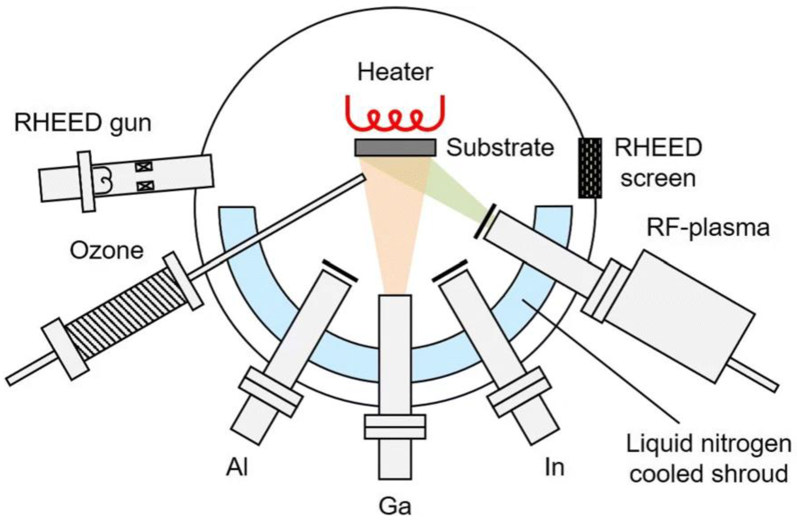
2. Molecular Beam Epitaxy (MBE)
2.1. Introduction
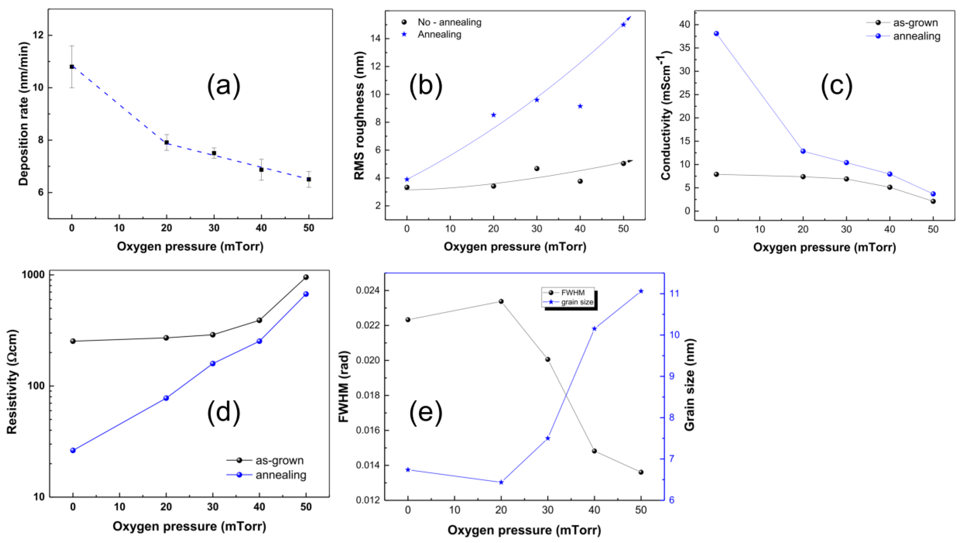
2.2. Effects of Growth Conditions on Film Properties
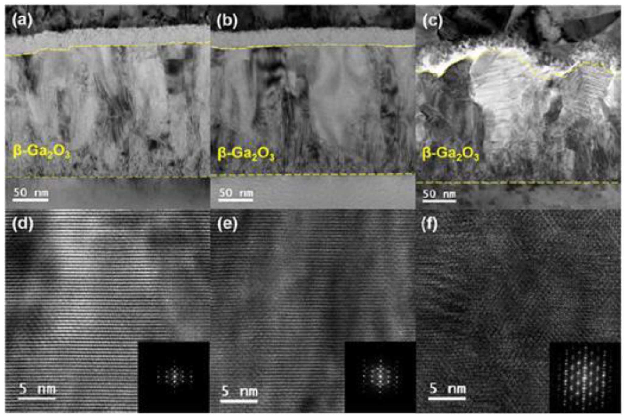
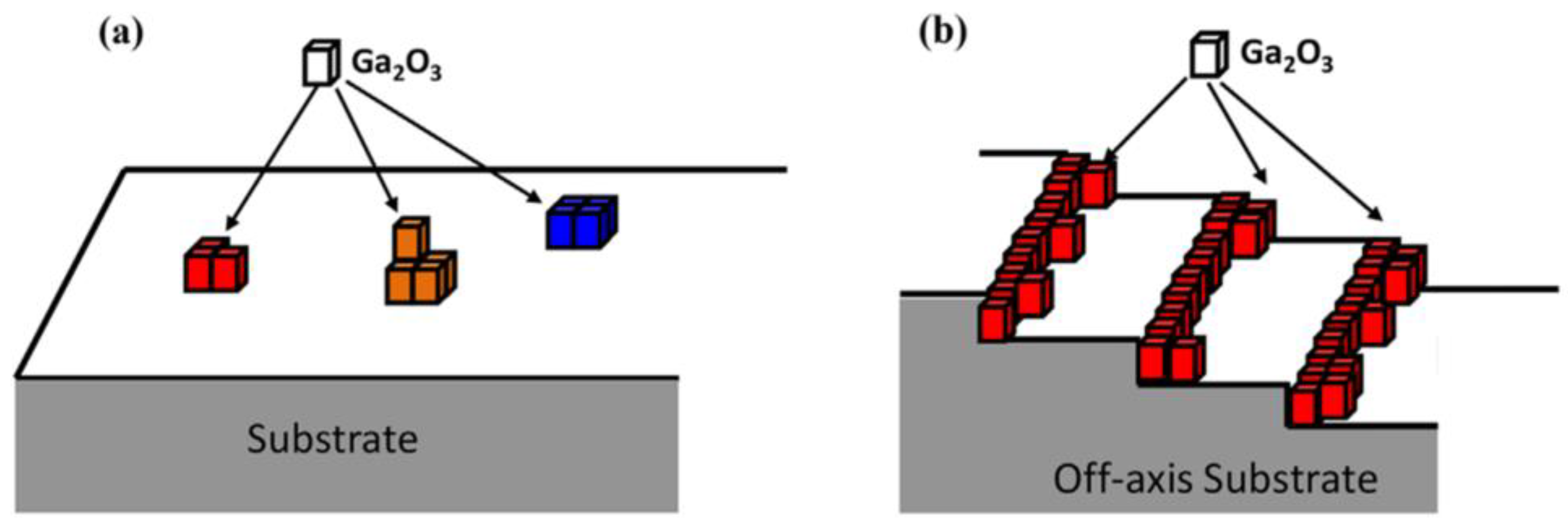
2.2.1. Morphology
- Substrate
- 2.
- Growth temperature
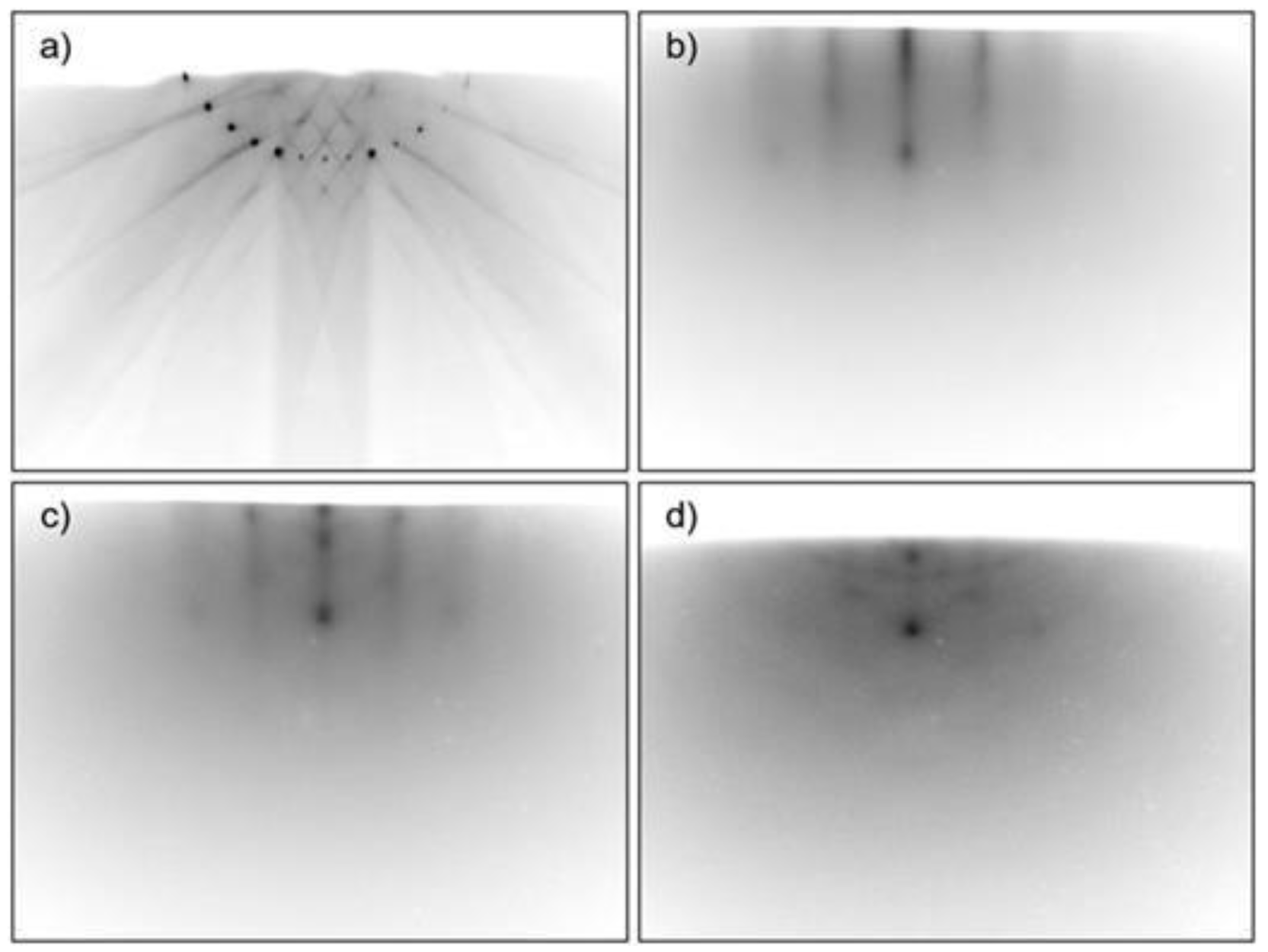
- 3.
- Ga flux

- 4.
- Other factors
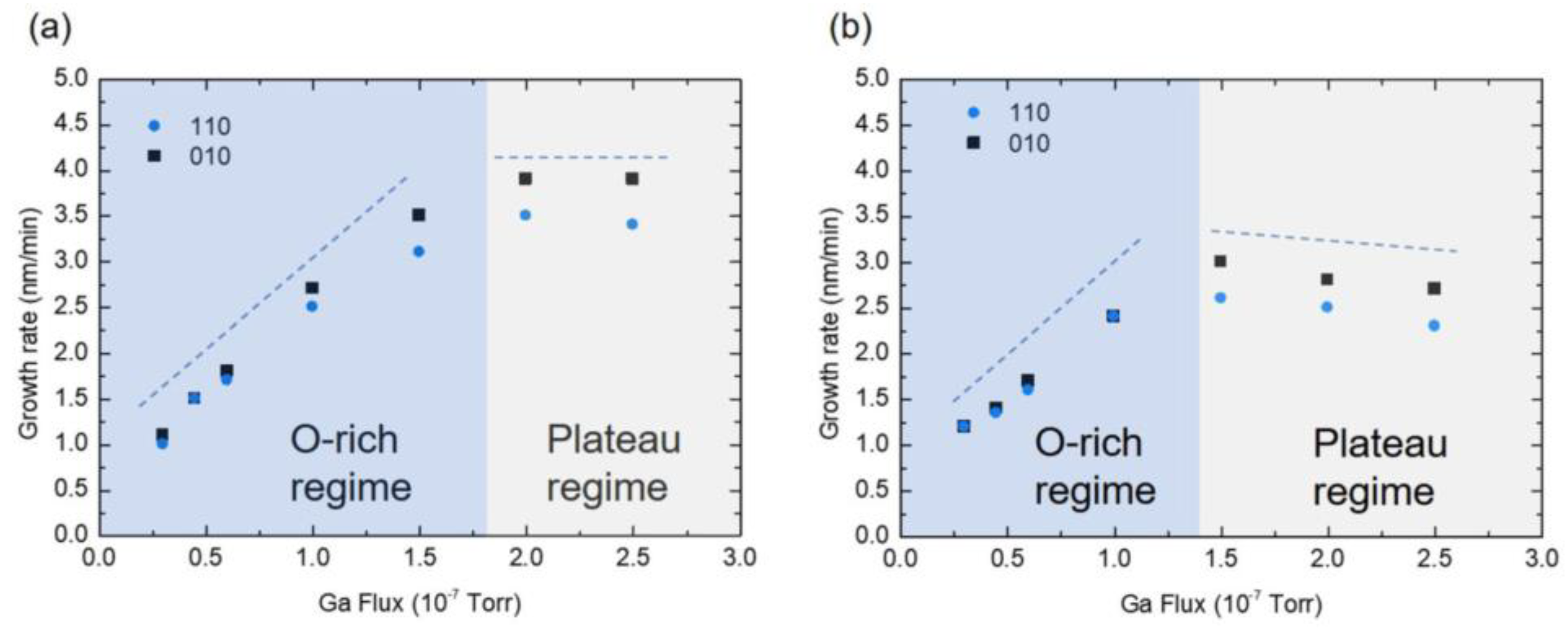
2.2.2. Growth Rate
2.2.3. Thermal Conductivity
2.3. Doping
2.4. Summary and Future Prospects
3. Metalorganic Chemical Vapor Deposition (MOCVD)
3.1. Introduction
3.2. Chemical Kinetics of the MOCVD

3.3. Effects of Growth Conditions on Film Properties
3.3.1. Effects of Growth Temperature

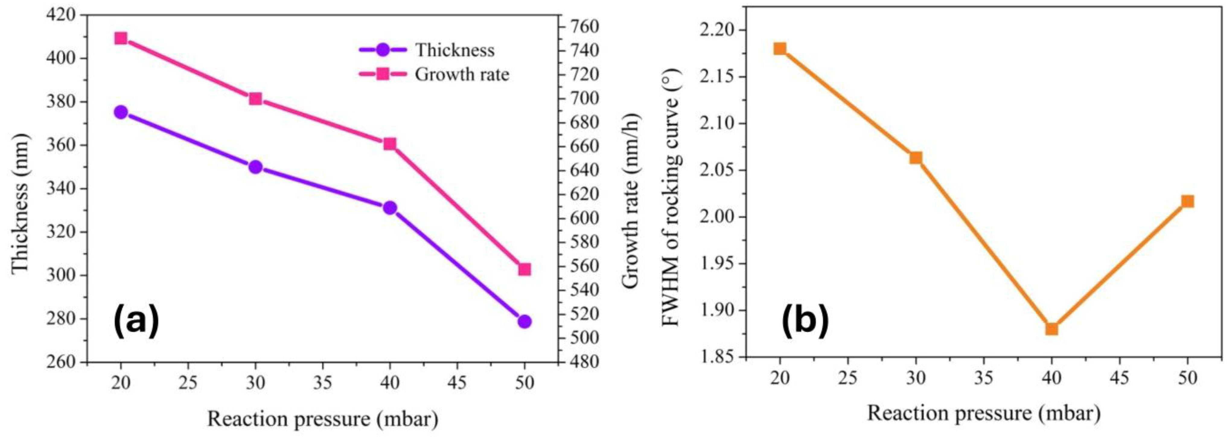
3.3.2. Effects of Reactor Pressure

3.3.3. Effects of Different Substrate Orientations on Homoepitaxy
3.3.4. Effects of Different Gallium Precursors and Their Growth Rate


3.3.5. Effects of Different Substrates
| Research | Optimum Growth Temperature (°C) | Optimum Growth Pressure | Substrate | Growth Rate (µm/h) | Optimum FWHM | Optimized RMS Roughness (nm) | Hall Mobility | Deposition Time (min) | Carrier Gas and Flow Rate | Precursor O2 Flow Rate | Gallium Precursor Flow Rate |
|---|---|---|---|---|---|---|---|---|---|---|---|
| TMGa Precursor | |||||||||||
| Li et al. (2020) [114] | 750 | 40 mbar | (01) β-Ga2O3 | 0.62 | 21.6 (arcsec) | 0.68 | - | 30 | Ar (6N)-10 sccm | (5N)400 sccm | |
| Mi et al. (2012) [136] | 650 | 20 Torr | MgO (110) | 0.076 | 0.59° | - | - | 360 | N2 (9N) | 50 sccm | 2.7 µ·mol/min |
| Alema et al. (2017) [91] | 900 | 40–120 Torr | (0001) C-sapphire | 10 | - | - | - | - | Ar (150 sccm) | 800 sccm | 50–109 µ·mol/min |
| Li et al. (2024) [137] | 750 | 20–50 mbar | Sapphire (0001) | ~0.1–0.75 | 2.18°–1.88° | 4.6–6.7 | - | 30 | - | (5N) | - |
| CaO et al. (2018) [117] | 660 | 20 Torr | Epi-GaN/sapphire | 0.25 | 0.5° | 0.76 | 300 | N2 (9N) | 50 sccm | 4.5 sccm | |
| Gogova et. al., (2022) [121] | 740 °C | 10 mbar–200 mbar | α-Al2O3 | 1.4 | - | - | - | 60 | Ar | 515 mL/min | 106 mol/min |
| Meng et al. (2022) [119] | 950 °C | 60 torr | Fe doped (010) Ga2O3 | 2.95 | - | ~1.23 | 190 cm2/V·s | 60 | - | 800 sccm | 58 µ·mol/min |
| Meng et al. (2024) [128] | TEGa: 880 °C; TMGa: 850–950 °C | 60 torr | (001) Ga2O3 | TEGa: 0.813; TMGa: 3.17 | - | ~2.56–10.2 | 85 cm2/V·s | 30–180 | Ar | TEGa: O2 = 400–1000 sccm; TMGa: O2 = 800 sccm | TEGa:12–31 µ·mol/min; TMGa: 58 µ·mol/min |
| Wagner et al. (2014) [138] | 750–850 °C | 5–100 mbar | (100) β-Ga2O3 | 0.18–0.48 | - | 6.5 | - | 30 | Ar | O2: 200–1500 sccm; H2O: 400–1500 sccm | 5 sccm |
| TEGa Precursor | |||||||||||
| Seo et al. (2023) [122] | 810 °C | (UID) GaN (002)/Al2O3 | - | - | 11.39 | - | 20 | Ar | - | - | |
| Tang et al. (2023) [139] | 800–900 °C | 10 KPa | β-Ga2O3 | 0.24–0.42 | 60 arcsec | 1.3 | 51 cm2/V·s | N2 | O2 | 68.2 µ·mol/min | |
| Meng et al. (2022) [140] | 880 | 60 | on-axis (100) Ga2O3 | 0.66 | 60 arcsec | 1.64 | 24 cm2/V·s | Shroud gas: Ar (300–2800 sccm) | O2: 800 sccm | VI/III ratio: 1150–2989 | |
| Chen et al. (2015) [118] | 550 | 5000 Pa | GaAs (100) | 0.89 | - | 6.41 | 60 | Ar (5N) | (5N) 50 sccm | 150 sccm | |
| Alema et al. (2020) [141] | 700 °C < T > 1100 °C | 75 Torr < P > 500 Torr | Fe doped β-Ga2O3 (010) | - | 41 arcsec | 0.8 | 153 cm2/V s | - | Ar (6N) | N2O or oxygen (5N) | - |
| Zhang et al. (2019) [94] | - | - | β-Ga2O3 (010) | 0.8 | 41.1 arcsec | 0.8 | 176 cm2/V s | - | Ar (6N) | O2 (5N) | - |
| Yuea et. al. (2022) [142] | 590 °C | 25 torr | C-sapphire (0001) | 0.775 | 1.71° | 5.45 | - | 120 | Ar (6N) | 2000 sccm | 350 sccm |
| Alema et al. (2020) [95] | - | - | β-Ga2O3 (010) | ~1 | ~43 arcsec | 0.8–13.4 | >104 cm2/V·s | - | Ar (6N) | O2 and H2O vapor source (0–250 ppm) | - |
| Chou et al. (2021) [126] | 825 °C | 25 mbar | β-Ga2O3 (100) | ~1 | 30 arcsec | 0.3–0.5 | 144 cm2/V·s | - | Ar (5N): 235 mmol/min | O2 (22 mmol/min) | 73 µ·mol/min |
| Feng et al. (2019) [92] | 880 °C | 60 torr | Fe doped Ga2O3 | 0.65–0.7 | - | ~1.7 | ~140 cm2/V·s | - | - | - | VI/III ratio = 1150 |
3.4. Doping
3.5. Summary and Future Prospects
4. Halide Vapor Phase Epitaxy (HVPE)
4.1. Introduction
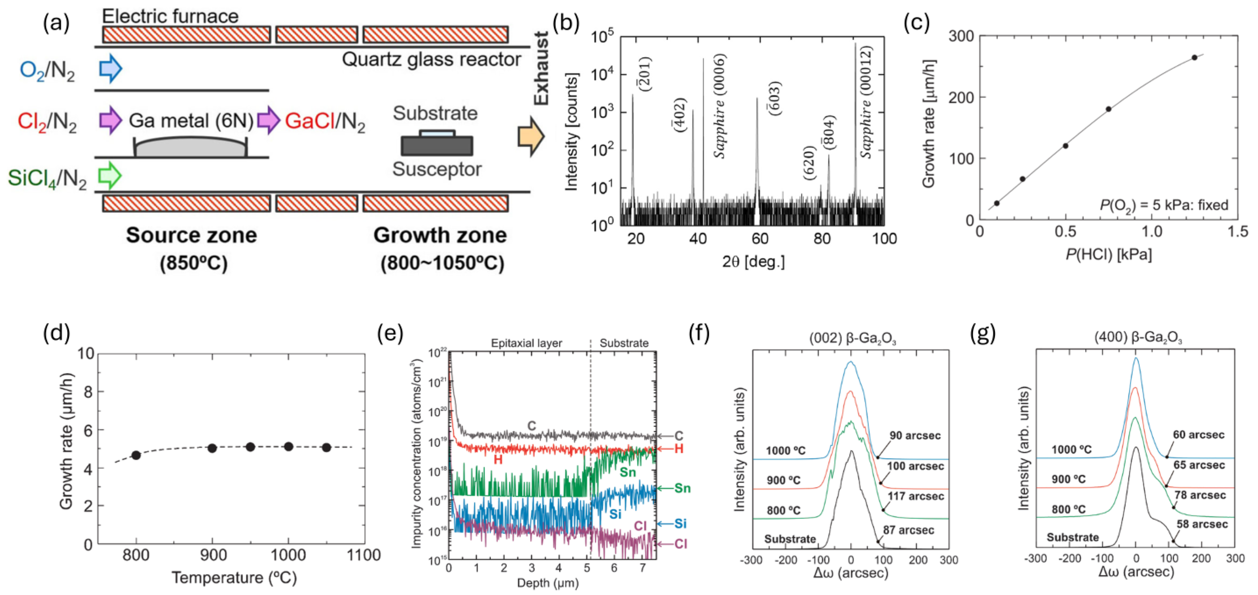
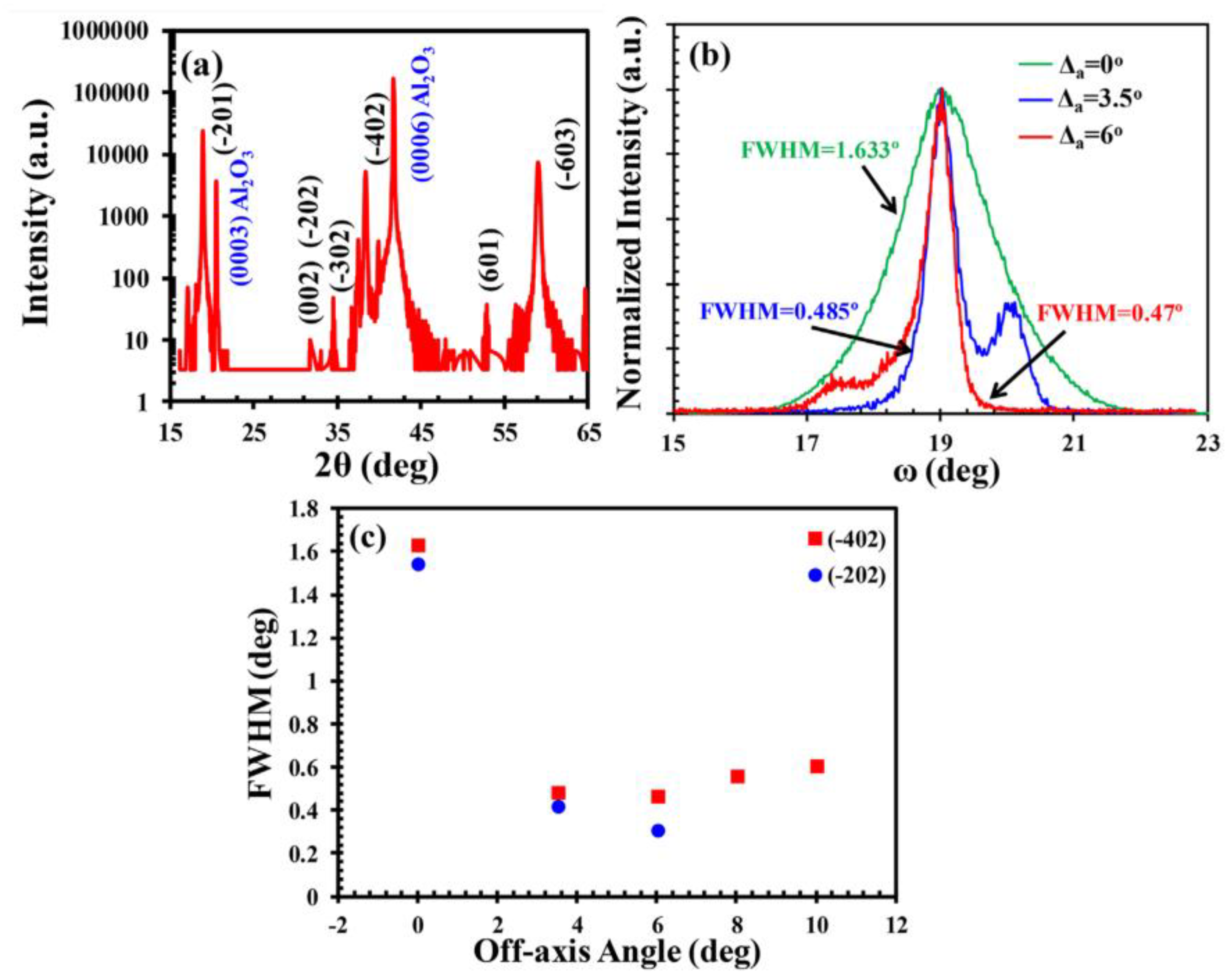
4.2. Effects of Growth Conditions on Film Properties

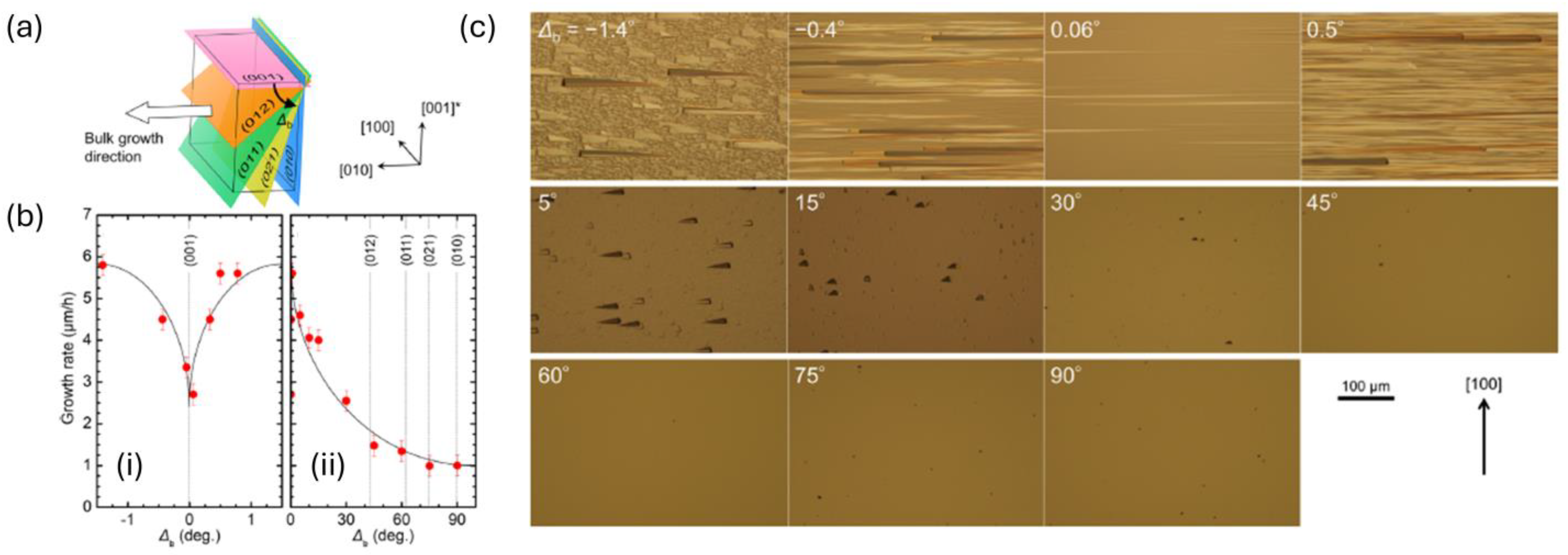
4.3. Selective Area Growth of Ga2O3 Using HVPE

4.4. Device Based on HVPE-Grown β-Ga2O3 Layers
4.5. Other Phases of Ga2O3 Growth Using HVPE
5. Mist Chemical Vapor Deposition (Mist-CVD)
5.1. Introduction

5.2. Effects of Growth Conditions and Progress
5.2.1. Epilayer Quality


5.2.2. Carrier Transportation
5.2.3. Devices
5.3. Summary
6. Pulsed Laser Deposition (PLD)
6.1. Introduction

6.2. Effects of Growth Conditions on Film Properties
6.2.1. Homoepitaxy

6.2.2. Heteroepitaxy
6.3. Growth Conditions
6.3.1. Temperature

6.3.2. Oxygen Partial Pressure
6.4. Doping
6.5. Applications

6.6. Summary and Future Prospects
7. Low-Pressure Chemical Vapor Deposition (LPCVD)
7.1. Introduction

7.2. LPCVD Growth of β-Ga2O3
7.2.1. Growth on Sapphire

7.2.2. Growth on Other Substrates
7.2.3. Homoepitaxy
7.2.4. Nanostructure Growth

7.3. Summary and Future Prospects
| Researcher | Temperature (°C) | Growth Rate (μm/h) | RMS Roughness (nm) | FWHM (°) | Hall Mobility (cm2/V·s) | O2 Flow Rate (sccm) | Pressure (torr) | Substrate to Crucible (cm) | Substrate |
|---|---|---|---|---|---|---|---|---|---|
| [93,230,243,251] | 900 | 10 | - | 0.47 | 106.6 | - | 4 | - | Sapphire |
| 900 | 1.9 | 1.3 | 0.013 | 76 | - | 4 | - | Ga2O3 (010) | |
| 900 | 1.2 | 4 | 0.043 | 42 | - | 4 | - | Ga2O3 (001) | |
| 800 | 1.7 | - | - | 42.35 | - | - | - | sapphire | |
| 950 | 1.3 | 16.9 | - | - | - | - | - | Ga2O3 | |
| Joshi et al. [226,231] | 825 | 3 | 6 | - | - | 20 | 1.5 | 12 | sapphire |
| 875 | 6 | 4.56 | 2.1 | - | 5 | 0.75 | 5 | sapphire | |
| 925 | 6 | 5.35 | 1.5 | - | 5 | 0.75 | 5 | sapphire | |
| Feng et al. [244] | 900 | 10–30 | - | - | 50–63 | 15–30 | - | - | sapphire |
| 820–940 | 1.5–20 | - | - | 45–70 | - | - | - | sapphire | |
| 900 | 7–13.5 | - | - | 50–65 | - | 2–12 | - | Sapphire | |
| 900 | 14–10 | - | - | - | 15 | 1.7 | 2–7 | sapphire | |
| 1000 | 12 | - | - | 126 | 20 | - | 2 | Sapphire | |
| 1050 | - | 3 | - | 156 | 30 | - | 2 | Ga2O3 | |
| Jiao et al. [273] | 800–900 | 0.72 | 1.18–12 | 1.82–1.7 | - | - | 0.37 | - | sapphire |
| Zhang et al. [246] | 1000 | 12 | - | - | 126 | 20 | - | 2 | Sapphire |
| 1050 | - | 3 | - | 156 | 30 | - | 2 | Ga2O3 | |
| Wu et al. [247] | 900 | 1.5 | - | 1.6 | - | 25 | - | 20 | sapphire |
| Hu et al. [250] | 650 | - | 2.25 | 1.37 | - | - | 0.75 | - | 4H-SiC |
| Akyoler et al. [245] | 850–925 | 0.49–3.421 | 40–0.5 | 0.09–0.2 | - | 8 | 0.7 | 11.5 | sapphire |
| Karim et al. [235] | 920 | 5.1 | - | 1.1 | 5.1 | 15 | - | - | Diamond |
| Ranga et al. [274] | 800–900 | 22 | - | - | 20–5 | 3–5 | 0.5–2 | - | Ga2O3 |
8. Discussion
| Samples | Ga2O3/SiO2/Si | Ga2O3/Si | Ga2O3/Al2O3 | Ga2O3/Al2O3 | Ga2O3/Al2O3 | Ga2O3/Al2O3 | Ga2O3/Al2O3 |
|---|---|---|---|---|---|---|---|
| Growth approach | PEALD | MOCVD | Mist CVD | Mist CVD | Mist CVD | HVPE | MOCVD |
| Size (in.) | 4 | 8 | 4 | 2 | 2 | 2 | 2 |
| Thickness (nm) | 10–30 | 90 | 230 | 187 | 210 | 1100 | 1550 |
| Inhomogeneity (%) | 1.5–2 | 3.3 | - | 20 | 3 | 2.6 | 1.8 |
| SD (nm) | - | - | 28 | - | 5.7 | 50 | 28 |
| Ref. | [275] | [276] | [193] | [195] | [277] | [278] | [142] |
Author Contributions
Funding
Institutional Review Board Statement
Informed Consent Statement
Data Availability Statement
Conflicts of Interest
References
- Waseem, A.; Ren, Z.; Huang, H.-C.; Nguyen, K.; Wu, X.; Li, X. A Review of Recent Progress in β-Ga2O3 Epitaxial Growth: Effect of Substrate Orientation and Precursors in Metal–Organic Chemical Vapor Deposition. Phys. Status Solidi (a) 2023, 220, 2200616. [Google Scholar] [CrossRef]
- Casady, J.B.; Johnson, R.W. Status of silicon carbide (SiC) as a wide-bandgap semiconductor for high-temperature applications: A review. Solid-State Electron. 1996, 39, 1409–1422. [Google Scholar] [CrossRef]
- Yuan, M.; Xie, Q.; Fu, K.; Hossain, T.; Niroula, J.; Greer, J.A.; Chowdhury, N.; Zhao, Y.; Palacios, T. GaN Ring Oscillators Operational at 500 °C Based on a GaN-on-Si Platform. IEEE Electron Device Lett. 2022, 43, 1842–1845. [Google Scholar] [CrossRef]
- Liang, Y.C.; Sun, R.; Yeo, Y.-C.; Zhao, C. Development of GaN Monolithic Integrated Circuits for Power Conversion. In Proceedings of the 2019 IEEE Custom Integrated Circuits Conference (CICC), Austin, TX, USA, 14–17 April 2019; IEEE: Piscataway, NJ, USA, 2019; pp. 1–4. [Google Scholar]
- Waseem, A.; Johar, M.A.; Hassan, M.A.; Bagal, I.V.; Ha, J.-S.; Lee, J.K.; Ryu, S.-W. Effect of crystal orientation of GaN/V2O5 core-shell nanowires on piezoelectric nanogenerators. Nano Energy 2019, 60, 413–423. [Google Scholar] [CrossRef]
- Waseem, A.; Johar, M.A.; Hassan, M.A.; Bagal, I.V.; Abdullah, A.; Ha, J.-S.; Lee, J.K.; Ryu, S.-W. GaN Nanowire Growth Promoted by In–Ga–Au Alloy Catalyst with Emphasis on Agglomeration Temperature and In Composition. ACS Omega 2021, 6, 3173–3185. [Google Scholar] [CrossRef]
- Pu, T.; Younis, U.; Chiu, H.-C.; Xu, K.; Kuo, H.-C.; Liu, X. Review of Recent Progress on Vertical GaN-Based PN Diodes. Nanoscale Res. Lett. 2021, 16, 101. [Google Scholar] [CrossRef]
- Sun, R.; Balog, A.R.; Yang, H.; Alem, N.; Scarpulla, M.A. Degradation of β-Ga2O3 Vertical Ni/Au Schottky Diodes Under Forward Bias. IEEE Electron Device Lett. 2023, 44, 725–728. [Google Scholar] [CrossRef]
- Xu, M.; Wang, D.; Fu, K.; Mudiyanselage, D.H.; Fu, H.; Zhao, Y. A review of ultrawide bandgap materials: Properties, synthesis and devices. Oxf. Open Mater. Sci. 2022, 2, itac004. [Google Scholar] [CrossRef]
- Yim, W.M.; Stofko, E.J.; Zanzucchi, P.J.; Pankove, J.I.; Ettenberg, M.; Gilbert, S.L. Epitaxially grown AlN and its optical band gap. J. Appl. Phys. 1973, 44, 292–296. [Google Scholar] [CrossRef]
- Mallesham, B.; Roy, S.; Bose, S.; Nair, A.N.; Sreenivasan, S.; Shutthanandan, V.; Ramana, C.V. Crystal Chemistry, Band-Gap Red Shift, and Electrocatalytic Activity of Iron-Doped Gallium Oxide Ceramics. ACS Omega 2020, 5, 104–112. [Google Scholar] [CrossRef]
- Fu, K.; Luo, S.; Fu, H.; Hatch, K.; Alugubelli, S.R.; Liu, H.; Li, T.; Xu, M.; Mei, Z.; He, Z.; et al. GaN-Based Threshold Switching Behaviors at High Temperatures Enabled by Interface Engineering for Harsh Environment Memory Applications. IEEE Trans. Electron Devices 2023, 71, 1–5. [Google Scholar] [CrossRef]
- Chatterjee, B.; Zeng, K.; Nordquist, C.D.; Singisetti, U.; Choi, S. Device-Level Thermal Management of Gallium Oxide Field-Effect Transistors. IEEE Trans. Compon. Packag. Manuf. Technol. 2019, 9, 2352–2365. [Google Scholar] [CrossRef]
- Higashiwaki, M.; Sasaki, K.; Murakami, H.; Kumagai, Y.; Koukitu, A.; Kuramata, A.; Masui, T.; Yamakoshi, S. Recent progress in Ga2O3 power devices. Semicond. Sci. Technol. 2016, 31, 034001. [Google Scholar] [CrossRef]
- Pearton, S.J.; Ren, F.; Tadjer, M.; Kim, J. Perspective: Ga2O3 for ultra-high power rectifiers and MOSFETS. J. Appl. Phys. 2018, 124, 220901. [Google Scholar] [CrossRef]
- Pearton, S.J.; Yang, J.; Cary, P.H.; Ren, F.; Kim, J.; Tadjer, M.J.; Mastro, M.A. A review of Ga2O3 materials, processing, and devices. Appl. Phys. Rev. 2018, 5, 011301. [Google Scholar] [CrossRef]
- Ogita, M.; Higo, K.; Nakanishi, Y.; Hatanaka, Y. Ga2O3 thin film for oxygen sensor at high temperature. Appl. Surf. Sci. 2001, 175–176, 721–725. [Google Scholar] [CrossRef]
- Mazeina, L.; Perkins, F.K.; Bermudez, V.M.; Arnold, S.P.; Prokes, S.M. Functionalized Ga2O3 Nanowires as Active Material in Room Temperature Capacitance-Based Gas Sensors. Langmuir 2010, 26, 13722–13726. [Google Scholar] [CrossRef] [PubMed]
- Lin, H.-J.; Gao, H.; Gao, P.-X. UV-enhanced CO sensing using Ga2O3-based nanorod arrays at elevated temperature. Appl. Phys. Lett. 2017, 110, 043101. [Google Scholar] [CrossRef]
- Galazka, Z.; Uecker, R.; Irmscher, K.; Albrecht, M.; Klimm, D.; Pietsch, M.; Brützam, M.; Bertram, R.; Ganschow, S.; Fornari, R. Czochralski growth and characterization of β-Ga2O3 single crystals. Cryst. Res. Technol. 2010, 45, 1229–1236. [Google Scholar] [CrossRef]
- Kuramata, A.; Koshi, K.; Watanabe, S.; Yamaoka, Y.; Masui, T.; Yamakoshi, S. High-quality β-Ga2O3 single crystals grown by edge-defined film-fed growth. Jpn. J. Appl. Phys. 2016, 55, 1202A2. [Google Scholar] [CrossRef]
- Teherani, F.H.; Rogers, D.J.; Sandana, V.E.; Bove, P.; Ton-That, C.; Lem, L.L.C.; Chikoidze, E.; Neumann-Spallart, M.; Dumont, Y.; Huynh, T.; et al. A Study into the Impact of Sapphire Substrate Orientation on the Properties of Nominally-Undoped β-Ga2O3 Thin Films Grown by Pulsed Laser Deposition; Teherani, F.H., Look, D.C., Rogers, D.J., Eds.; OPTO: San Francisco, CA, USA, 2017; p. 101051R. [Google Scholar]
- Pomeroy, J.W.; Uren, M.J.; Lambert, B.; Kuball, M. Operating channel temperature in GaN HEMTs: DC versus RF accelerated life testing. Microelectron. Reliab. 2015, 55, 2505–2510. [Google Scholar] [CrossRef]
- Guo, Z.; Verma, A.; Wu, X.; Sun, F.; Hickman, A.; Masui, T.; Kuramata, A.; Higashiwaki, M.; Jena, D.; Luo, T. Anisotropic thermal conductivity in single crystal β-gallium oxide. Appl. Phys. Lett. 2015, 106, 111909. [Google Scholar] [CrossRef]
- Rahaman, I.; Ellis, H.D.; Fu, K. Robust Diamond β-Ga2O3 Hetero-p-n-junction Via Mechanically Integrating Their Building Blocks. arXiv 2023, arXiv:2311.16323. [Google Scholar] [CrossRef]
- Cheng, Z.; Wheeler, V.D.; Bai, T.; Shi, J.; Tadjer, M.J.; Feygelson, T.; Hobart, K.D.; Goorsky, M.S.; Graham, S. Integration of polycrystalline Ga2O3 on diamond for thermal management. Appl. Phys. Lett. 2020, 116, 062105. [Google Scholar] [CrossRef]
- Matsumae, T.; Kurashima, Y.; Umezawa, H.; Tanaka, K.; Ito, T.; Watanabe, H.; Takagi, H. Low-temperature direct bonding of β-Ga2O3 and diamond substrates under atmospheric conditions. Appl. Phys. Lett. 2020, 116, 141602. [Google Scholar] [CrossRef]
- Smith, R.J.; Bryant, R.G. Metal substitutions incarbonic anhydrase: A halide ion probe study. Biochem. Biophys. Res. Commun. 1975, 66, 1281–1286. [Google Scholar] [CrossRef] [PubMed]
- Cheng, Z.; Yates, L.; Shi, J.; Tadjer, M.J.; Hobart, K.D.; Graham, S. Thermal conductance across β-Ga2O3-diamond van der Waals heterogeneous interfaces. APL Mater. 2019, 7, 031118. [Google Scholar] [CrossRef]
- Malakoutian, M.; Song, Y.; Yuan, C.; Ren, C.; Lundh, J.S.; Lavelle, R.M.; Brown, J.E.; Snyder, D.W.; Graham, S.; Choi, S.; et al. Polycrystalline diamond growth on β-Ga2O3 for thermal management. Appl. Phys. Express 2021, 14, 055502. [Google Scholar] [CrossRef]
- Mandal, S.; Arts, K.; Knoops, H.C.M.; Cuenca, J.A.; Klemencic, G.M.; Williams, O.A. Surface zeta potential and diamond growth on gallium oxide single crystal. Carbon 2021, 181, 79–86. [Google Scholar] [CrossRef]
- Rahaman, I.; Sultana, M.; Medina, R.; Emu, I.H.; Haque, A. Optimization of Electrostatic Seeding Technique for Wafer-Scale Diamond Fabrication on Β-Ga2O3. Mater. Sci. Semicond. Process. 2024, 108808. Available online: https://www.researchgate.net/publication/381176441_Optimization_of_Electrostatic_Seeding_Technique_for_Wafer-Scale_Diamond_Fabrication_on_B-Ga2o3 (accessed on 1 January 2020). [CrossRef]
- Shinohara, D.; Fujita, S. Heteroepitaxy of Corundum-Structured α-Ga2O3 Thin Films on α-Al2O3 Substrates by Ultrasonic Mist Chemical Vapor Deposition. Jpn. J. Appl. Phys. 2008, 47, 7311. [Google Scholar] [CrossRef]
- Kawaharamura, T.; Dang, G.T.; Furuta, M. Successful Growth of Conductive Highly Crystalline Sn-Doped α-Ga2O3 Thin Films by Fine-Channel Mist Chemical Vapor Deposition. Jpn. J. Appl. Phys. 2012, 51, 040207. [Google Scholar] [CrossRef]
- Sasaki, K.; Higashiwaki, M.; Kuramata, A.; Masui, T.; Yamakoshi, S. MBE grown Ga2O3 and its power device applications. J. Cryst. Growth 2013, 378, 591–595. [Google Scholar] [CrossRef]
- Sasaki, K.; Higashiwaki, M.; Kuramata, A.; Masui, T.; Yamakoshi, S. Growth temperature dependences of structural and electrical properties of Ga2O3 epitaxial films grown on β-Ga2O3 (010) substrates by molecular beam epitaxy. J. Cryst. Growth 2014, 392, 30–33. [Google Scholar] [CrossRef]
- Zhang, F.B.; Saito, K.; Tanaka, T.; Nishio, M.; Guo, Q.X. Structural and optical properties of Ga2O3 films on sapphire substrates by pulsed laser deposition. J. Cryst. Growth 2014, 387, 96–100. [Google Scholar] [CrossRef]
- Yao, Y.; Okur, S.; Lyle, L.A.M.; Tompa, G.S.; Salagaj, T.; Sbrockey, N.; Davis, R.F.; Porter, L.M. Growth and characterization of α-, β-, and ϵ-phases of Ga2O3 using MOCVD and HVPE techniques. Mater. Res. Lett. 2018, 6, 268–275. [Google Scholar] [CrossRef]
- Murakami, H.; Nomura, K.; Goto, K.; Sasaki, K.; Kawara, K.; Thieu, Q.T.; Togashi, R.; Kumagai, Y.; Higashiwaki, M.; Kuramata, A.; et al. Homoepitaxial growth of β-Ga2O3 layers by halide vapor phase epitaxy. Appl. Phys. Express 2015, 8, 015503. [Google Scholar] [CrossRef]
- Park, J.-H.; McClintock, R.; Razeghi, M. Ga2O3 metal-oxide-semiconductor field effect transistors on sapphire substrate by MOCVD. Semicond. Sci. Technol. 2019, 34, 08LT01. [Google Scholar] [CrossRef]
- Boschi, F.; Bosi, M.; Berzina, T.; Buffagni, E.; Ferrari, C.; Fornari, R. Hetero-epitaxy of ε-Ga2O3 layers by MOCVD and ALD. J. Cryst. Growth 2016, 443, 25–30. [Google Scholar] [CrossRef]
- Sun, H.; Li, K.-H.; Castanedo, C.G.T.; Okur, S.; Tompa, G.S.; Salagaj, T.; Lopatin, S.; Genovese, A.; Li, X. HCl Flow-Induced Phase Change of α-, β-, and ε-Ga2O3 Films Grown by MOCVD. Cryst. Growth Des. 2018, 18, 2370–2376. [Google Scholar] [CrossRef]
- Feng, Z.; Bhuiyan, A.F.M.A.U.; Xia, Z.; Moore, W.; Chen, Z.; McGlone, J.F.; Daughton, D.R.; Arehart, A.R.; Ringel, S.A.; Rajan, S.; et al. Probing Charge Transport and Background Doping in Metal-Organic Chemical Vapor Deposition-Grown (010) β-Ga2O3. Phys. Status Solidi RRL—Rapid Res. Lett. 2020, 14, 2000145. [Google Scholar] [CrossRef]
- Zhang, J.; Shi, J.; Qi, D.-C.; Chen, L.; Zhang, K.H.L. Recent progress on the electronic structure, defect, and doping properties of Ga2O3. APL Mater. 2020, 8, 020906. [Google Scholar] [CrossRef]
- Zhang, Z.-C.; Wu, Y.; Lu, C.; Ahmed, S. Electron mobility in β-Ga2O3: An ensemble Monte Carlo study. Appl. Phys. A 2018, 124, 637. [Google Scholar] [CrossRef]
- Yoshioka, S.; Hayashi, H.; Kuwabara, A.; Oba, F.; Matsunaga, K.; Tanaka, I. Structures and energetics of Ga2O3 polymorphs. J. Phys. Condens. Matter 2007, 19, 346211. [Google Scholar] [CrossRef]
- Kaneko, K.; Uno, K.; Jinno, R.; Fujita, S. Prospects for phase engineering of semi-stable Ga2O3 semiconductor thin films using mist chemical vapor deposition. J. Appl. Phys. 2022, 131, 090902. [Google Scholar] [CrossRef]
- Peelaers, H.; Varley, J.B.; Speck, J.S.; Van De Walle, C.G. Structural and electronic properties of Ga2O3-Al2O3 alloys. Appl. Phys. Lett. 2018, 112, 242101. [Google Scholar] [CrossRef]
- Bhuiyan, A.F.M.A.U.; Feng, Z.; Huang, H.-L.; Meng, L.; Hwang, J.; Zhao, H. MOCVD growth and band offsets of κ-phase Ga2O3 on c-plane sapphire, GaN- and AlN-on-sapphire, and (100) YSZ substrates. J. Vac. Sci. Technol. A 2022, 40, 062704. [Google Scholar] [CrossRef]
- Cora, I.; Mezzadri, F.; Boschi, F.; Bosi, M.; Čaplovičová, M.; Calestani, G.; Dódony, I.; Pécz, B.; Fornari, R. The real structure of ε-Ga2O3 and its relation to κ-phase. CrystEngComm 2017, 19, 1509–1516. [Google Scholar] [CrossRef]
- Bhuiyan, A.F.M.A.U.; Feng, Z.; Huang, H.-L.; Meng, L.; Hwang, J.; Zhao, H. Metalorganic chemical vapor deposition of α-Ga2O3 and α-(AlxGa1−x)2O3 thin films on m-plane sapphire substrates. APL Mater. 2021, 9, 101109. [Google Scholar] [CrossRef]
- Maccioni, M.B.; Fiorentini, V. Phase diagram and polarization of stable phases of (Ga1−xInx)2O3. Appl. Phys. Express 2016, 9, 041102. [Google Scholar] [CrossRef]
- Playford, H.Y.; Hannon, A.C.; Tucker, M.G.; Dawson, D.M.; Ashbrook, S.E.; Kastiban, R.J.; Sloan, J.; Walton, R.I. Characterization of Structural Disorder in γ-Ga2O3. J. Phys. Chem. C 2014, 118, 16188–16198. [Google Scholar] [CrossRef]
- Kato, T.; Nishinaka, H.; Shimazoe, K.; Kanegae, K.; Yoshimoto, M. Demonstration of Bixbyite-Structured δ-Ga2O3 Thin Films Using β-Fe2O3 Buffer Layers by Mist Chemical Vapor Deposition. ACS Appl. Electron. Mater. 2023, 5, 1715–1720. [Google Scholar] [CrossRef]
- Bhuiyan, A.F.M.A.U.; Feng, Z.; Meng, L.; Zhao, H. Tutorial: Metalorganic chemical vapor deposition of β-Ga2O3 thin films, alloys, and heterostructures. J. Appl. Phys. 2023, 133, 211103. [Google Scholar] [CrossRef]
- Higashiwaki, M.; Sasaki, K.; Kuramata, A.; Masui, T.; Yamakoshi, S. Gallium oxide (Ga2O3) metal-semiconductor field-effect transistors on single-crystal β-Ga2O3 (010) substrates. Appl. Phys. Lett. 2012, 100, 013504. [Google Scholar] [CrossRef]
- Chae, S.; Mengle, K.; Bushick, K.; Lee, J.; Sanders, N.; Deng, Z.; Mi, Z.; Poudeu, P.F.P.; Paik, H.; Heron, J.T.; et al. Toward the predictive discovery of ambipolarly dopable ultra-wide-band-gap semiconductors: The case of rutile GeO2. Appl. Phys. Lett. 2021, 118, 260501. [Google Scholar] [CrossRef]
- Cho, K.J.; Chang, W.; Lee, H.-K.; Mun, J.K. β-Ga2O3 Schottky Barrier Diodes with Near-Zero Turn-on Voltage and Breakdown Voltage over 3.6 kV. Trans. Electr. Electron. Mater. 2024, 25, 365–369. [Google Scholar] [CrossRef]
- Mukhopadhyay, P.; Hatipoglu, I.; Sakthivel, T.S.; Hunter, D.A.; Edwards, P.R.; Martin, R.W.; Naresh-Kumar, G.; Seal, S.; Schoenfeld, W.V. High Figure-of-Merit Gallium Oxide UV Photodetector on Silicon by Molecular Beam Epitaxy: A Path toward Monolithic Integration. Adv. Photonics Res. 2021, 2, 2000067. [Google Scholar] [CrossRef]
- Sharma, S.; Meng, L.; Bhuiyan, A.F.M.A.U.; Feng, Z.; Eason, D.; Zhao, H.; Singisetti, U. Vacuum Annealed β-Ga2O3 Recess Channel MOSFETs With 8.56 kV Breakdown Voltage. IEEE Electron Device Lett. 2022, 43, 2029–2032. [Google Scholar] [CrossRef]
- Sheng, T.; Liu, X.-Z.; Qian, L.-X.; Xu, B.; Zhang, Y.-Y. Photoelectric properties of β-Ga2O3 thin films annealed at different conditions. Rare Met. 2022, 41, 1375–1379. [Google Scholar] [CrossRef]
- Zhao, B.; Li, K.; Liu, Q.; Liu, X. Ultrasensitive Self-Powered Deep-Ultraviolet Photodetector Based on In Situ Epitaxial Ga₂O₃/Bi₂Se₃ Heterojunction. IEEE Trans. Electron Devices 2022, 69, 1894–1899. [Google Scholar] [CrossRef]
- Mauze, A.; Speck, J. Plasma-Assisted Molecular Beam Epitaxy 1: Growth, Doping, and Heterostructures. In Gallium Oxide; Higashiwaki, M., Fujita, S., Eds.; Springer Series in Materials Science; Springer International Publishing: Berlin/Heidelberg, Germany, 2020; Volume 293, pp. 79–93. ISBN 978-3-030-37152-4. [Google Scholar]
- Sasaki, K.; Yamakoshi, S.; Kuramata, A. Ozone-Enhanced Molecular Beam Epitaxy. In Gallium Oxide; Higashiwaki, M., Fujita, S., Eds.; Springer Series in Materials Science; Springer International Publishing: Berlin/Heidelberg, Germany, 2020; Volume 293, pp. 123–140. ISBN 978-3-030-37152-4. [Google Scholar]
- Ardenghi, A.; Bierwagen, O.; Falkenstein, A.; Hoffmann, G.; Lähnemann, J.; Martin, M.; Mazzolini, P. Toward controllable Si-doping in oxide molecular beam epitaxy using a solid SiO source: Application to β-Ga2O3. Appl. Phys. Lett. 2022, 121, 042109. [Google Scholar] [CrossRef]
- Higashiwaki, M. β-Ga2O3 material properties, growth technologies, and devices: A review. AAPPS Bull. 2022, 32, 3. [Google Scholar] [CrossRef]
- Mazzolini, P.; Bierwagen, O. Towards smooth (010) β-Ga2O3 films homoepitaxially grown by plasma assisted molecular beam epitaxy: The impact of substrate offcut and metal-to-oxygen flux ratio. J. Phys. Appl. Phys. 2020, 53, 354003. [Google Scholar] [CrossRef]
- Hadamek, T.; Posadas, A.B.; Al-Quaiti, F.; Smith, D.J.; McCartney, M.R.; Dombrowski, E.; Demkov, A.A. Epitaxial growth of β-Ga2O3 on SrTiO3 (001) and SrTiO3-buffered Si (001) substrates by plasma-assisted molecular beam epitaxy. J. Appl. Phys. 2022, 131, 145702. [Google Scholar] [CrossRef]
- Itoh, T.; Mauze, A.; Zhang, Y.; Speck, J.S. Epitaxial growth of β-Ga2O3 on (110) substrate by plasma-assisted molecular beam epitaxy. Appl. Phys. Lett. 2020, 117, 152105. [Google Scholar] [CrossRef]
- Ngo, T.S.; Le, D.D.; Vuong, N.Q.; Hong, S.-K. Systematic Investigation of Growth and Properties of Ga2O3 Films on C-Plane Sapphire Substrates Prepared by Plasma-Assisted Molecular Beam Epitaxy. ECS J. Solid State Sci. Technol. 2022, 11, 035008. [Google Scholar] [CrossRef]
- Hadamek, T.; Posadas, A.B.; Al-Quaiti, F.; Smith, D.J.; McCartney, M.R.; Demkov, A.A. β-Ga2O3 on Si (001) grown by plasma-assisted MBE with γ-Al2O3 (111) buffer layer: Structural characterization. AIP Adv. 2021, 11, 045209. [Google Scholar] [CrossRef]
- Ohring, M. A Review of Materials Science. In Materials Science of Thin Films; Elsevier: Amsterdam, The Netherlands, 2002; pp. 1–56. ISBN 978-0-12-524975-1. [Google Scholar]
- Zhan, J.; Wu, Y.; Zeng, X.; Feng, B.; He, M.; He, G.; Ding, S. Study on the effects of Si-doping in molecular beam heteroepitaxial β-Ga2O3 films. J. Appl. Phys. 2024, 135, 105103. [Google Scholar] [CrossRef]
- Tian, C.; Zhang, C.; Lin, J.; Zhang, J.; Yang, W. Effect of Oxygen Precursors on Growth Mechanism in High-Quality β-Ga2O3 Epilayers on Sapphire by Molecular Beam Epitaxy and Related Solar-Blind Photodetectors. IEEE Sens. J. 2024, 24, 14109–14117. [Google Scholar] [CrossRef]
- Togashi, R.; Ishida, H.; Goto, K.; Higashiwaki, M.; Kumagai, Y. Thermodynamic analysis of β-Ga2O3 growth by molecular beam epitaxy. Jpn. J. Appl. Phys. 2023, 62, 015501. [Google Scholar] [CrossRef]
- Vogt, P.; Hensling, F.V.E.; Azizie, K.; Chang, C.S.; Turner, D.; Park, J.; McCandless, J.P.; Paik, H.; Bocklund, B.J.; Hoffman, G.; et al. Adsorption-controlled growth of Ga2O3 by suboxide molecular-beam epitaxy. APL Mater. 2021, 9, 031101. [Google Scholar] [CrossRef]
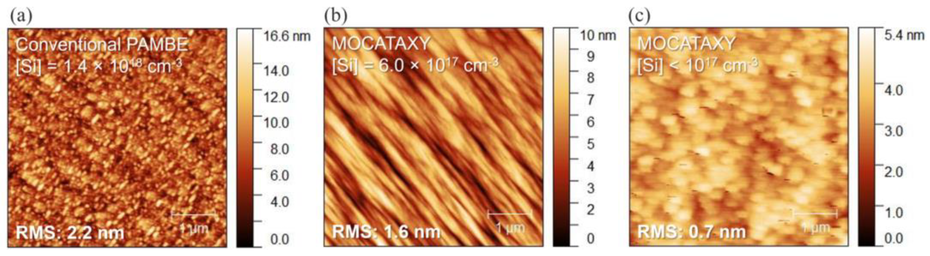
- Mauze, A.; Zhang, Y.; Itoh, T.; Wu, F.; Speck, J.S. Metal oxide catalyzed epitaxy (MOCATAXY) of β-Ga2O3 films in various orientations grown by plasma-assisted molecular beam epitaxy. APL Mater. 2020, 8, 021104. [Google Scholar] [CrossRef]
- Jiang, P.; Qian, X.; Li, X.; Yang, R. Three-dimensional anisotropic thermal conductivity tensor of single crystalline β-Ga2O3. Appl. Phys. Lett. 2018, 113, 232105. [Google Scholar] [CrossRef]
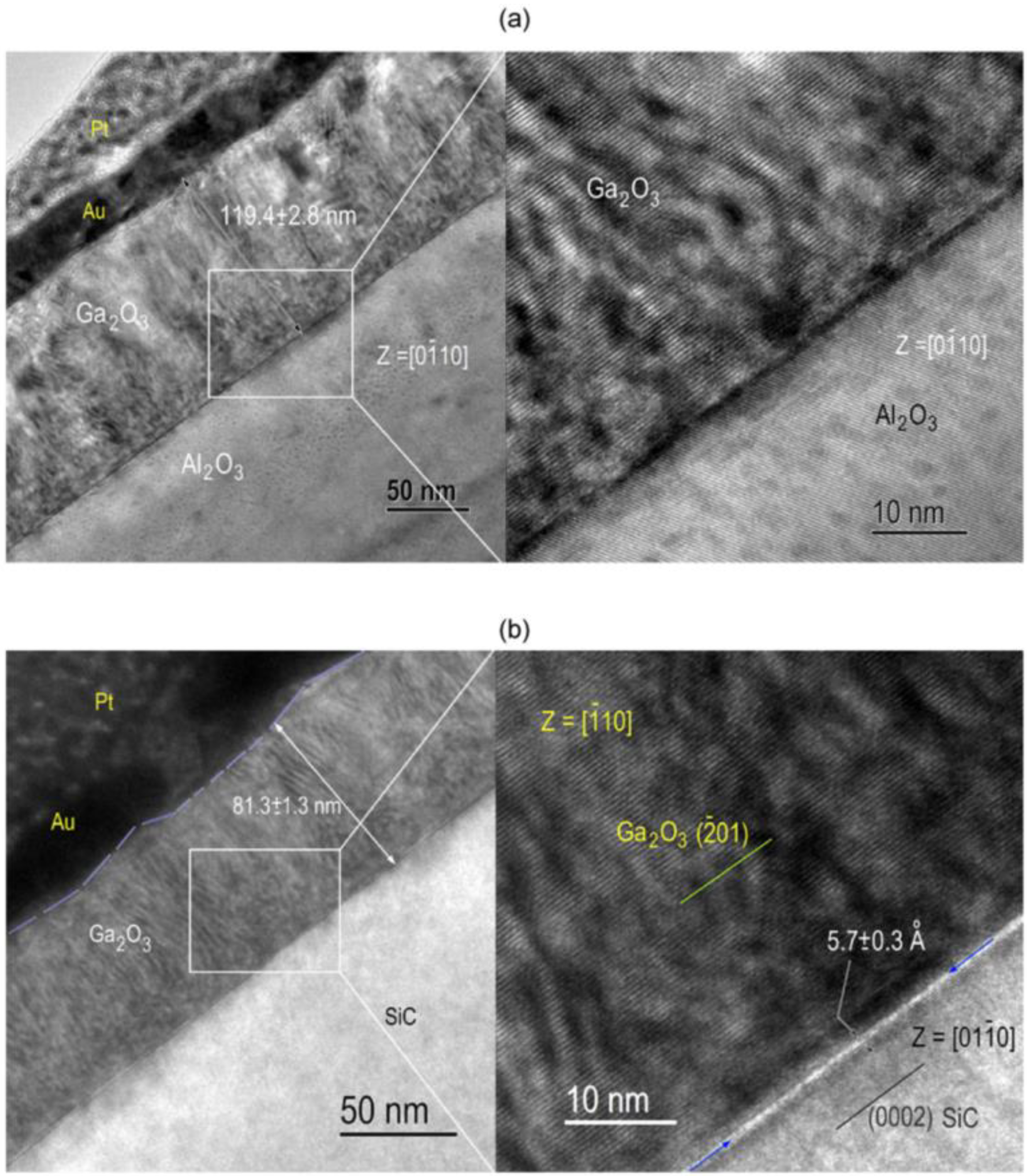
- Nepal, N.; Katzer, D.S.; Downey, B.P.; Wheeler, V.D.; Nyakiti, L.O.; Storm, D.F.; Hardy, M.T.; Freitas, J.A.; Jin, E.N.; Vaca, D.; et al. Heteroepitaxial growth of β-Ga2O3 films on SiC via molecular beam epitaxy. J. Vac. Sci. Technol. Vac. Surf. Films 2020, 38, 063406. [Google Scholar] [CrossRef]
- Vaca, D.; Barry, M.; Yates, L.; Nepal, N.; Katzer, D.S.; Downey, B.P.; Wheeler, V.; Nyakiti, L.; Meyer, D.J.; Graham, S.; et al. Measurements and numerical calculations of thermal conductivity to evaluate the quality of β-gallium oxide thin films grown on sapphire and silicon carbide by molecular beam epitaxy. Appl. Phys. Lett. 2022, 121, 042107. [Google Scholar] [CrossRef]
- McCandless, J.P.; Protasenko, V.; Morell, B.W.; Steinbrunner, E.; Neal, A.T.; Tanen, N.; Cho, Y.; Asel, T.J.; Mou, S.; Vogt, P.; et al. Controlled Si doping of β-Ga2O3 by molecular beam epitaxy. Appl. Phys. Lett. 2022, 121, 072108. [Google Scholar] [CrossRef]
- Kalarickal, N.K.; Xia, Z.; McGlone, J.; Krishnamoorthy, S.; Moore, W.; Brenner, M.; Arehart, A.R.; Ringel, S.A.; Rajan, S. Mechanism of Si doping in plasma assisted MBE growth of β-Ga2O3. Appl. Phys. Lett. 2019, 115, 152106. [Google Scholar] [CrossRef]
- Wen, Z.; Khan, K.; Zhai, X.; Ahmadi, E. Si doping of β-Ga2O3 by disilane via hybrid plasma-assisted molecular beam epitaxy. Appl. Phys. Lett. 2023, 122, 082101. [Google Scholar] [CrossRef]
- Azizie, K.; Hensling, F.V.E.; Gorsak, C.A.; Kim, Y.; Pieczulewski, N.A.; Dryden, D.M.; Senevirathna, M.K.I.; Coye, S.; Shang, S.-L.; Steele, J.; et al. Silicon-doped β-Ga2O3 films grown at 1 µm/h by suboxide molecular-beam epitaxy. APL Mater. 2023, 11, 041102. [Google Scholar] [CrossRef]
- Dheenan, A.V.; McGlone, J.F.; Kalarickal, N.K.; Huang, H.-L.; Brenner, M.; Hwang, J.; Ringel, S.A.; Rajan, S. β-Ga2O3 MESFETs with insulating Mg-doped buffer grown by plasma-assisted molecular beam epitaxy. Appl. Phys. Lett. 2022, 121, 113503. [Google Scholar] [CrossRef]
- Kumar, S.; Kamimura, T.; Lin, C.-H.; Nakata, Y.; Higashiwaki, M. Reduction in leakage current through interface between Ga2O3 epitaxial layer and substrate by ion implantation doping of compensating impurities. Appl. Phys. Lett. 2020, 117, 193502. [Google Scholar] [CrossRef]
- Mauze, A.; Zhang, Y.; Itoh, T.; Mates, T.E.; Peelaers, H.; Van De Walle, C.G.; Speck, J.S. Mg doping and diffusion in (010) β-Ga2O3 films grown by plasma-assisted molecular beam epitaxy. J. Appl. Phys. 2021, 130, 235301. [Google Scholar] [CrossRef]
- Mauze, A.; Zhang, Y.; Itoh, T.; Ahmadi, E.; Speck, J.S. Sn doping of (010) β-Ga2O3 films grown by plasma-assisted molecular beam epitaxy. Appl. Phys. Lett. 2020, 117, 222102. [Google Scholar] [CrossRef]
- Mazzolini, P.; Falkenstein, A.; Wouters, C.; Schewski, R.; Markurt, T.; Galazka, Z.; Martin, M.; Albrecht, M.; Bierwagen, O. Substrate-orientation dependence of β-Ga2O3 (100), (010), (001), and (2¯01) homoepitaxy by indium-mediated metal-exchange catalyzed molecular beam epitaxy (MEXCAT-MBE). APL Mater. 2020, 8, 011107. [Google Scholar] [CrossRef]
- Itoh, T.; Mauze, A.; Zhang, Y.; Speck, J.S. Continuous Si doping in (010) and (001) β-Ga2O3 films by plasma-assisted molecular beam epitaxy. APL Mater. 2023, 11, 041108. [Google Scholar] [CrossRef]
- Alema, F.; Hertog, B.; Osinsky, A.; Mukhopadhyay, P.; Toporkov, M.; Schoenfeld, W.V. Fast growth rate of epitaxial β–Ga2O3 by close coupled showerhead MOCVD. J. Cryst. Growth 2017, 475, 77–82. [Google Scholar] [CrossRef]
- Feng, Z.; Bhuiyan, A.F.M.A.U.; Karim, M.R.; Zhao, H. MOCVD homoepitaxy of Si-doped (010) β-Ga2O3 thin films with superior transport properties. Appl. Phys. Lett. 2019, 114, 250601. [Google Scholar] [CrossRef]
- Baldini, M.; Albrecht, M.; Fiedler, A.; Irmscher, K.; Schewski, R.; Wagner, G. Editors’ Choice—Si- and Sn-Doped Homoepitaxial β-Ga2O3 Layers Grown by MOVPE on (010)-Oriented Substrates. ECS J. Solid State Sci. Technol. 2017, 6, Q3040–Q3044. [Google Scholar] [CrossRef]
- Zhang, Y.; Alema, F.; Mauze, A.; Koksaldi, O.S.; Miller, R.; Osinsky, A.; Speck, J.S. MOCVD grown epitaxial β-Ga2O3 thin film with an electron mobility of 176 cm2/V s at room temperature. APL Mater. 2019, 7, 022506. [Google Scholar] [CrossRef]
- Alema, F.; Zhang, Y.; Mauze, A.; Itoh, T.; Speck, J.S.; Hertog, B.; Osinsky, A. H2O vapor assisted growth of β-Ga2O3 by MOCVD. AIP Adv. 2020, 10, 085002. [Google Scholar] [CrossRef]
- Bhattacharyya, A.; Ranga, P.; Roy, S.; Ogle, J.; Whittaker-Brooks, L.; Krishnamoorthy, S. Low temperature homoepitaxy of (010) β-Ga2O3 by metalorganic vapor phase epitaxy: Expanding the growth window. Appl. Phys. Lett. 2020, 117, 142102. [Google Scholar] [CrossRef]
- Alema, F.; Seryogin, G.; Osinsky, A.; Osinsky, A. Ge doping of β-Ga2O3 by MOCVD. APL Mater. 2021, 9, 091102. [Google Scholar] [CrossRef]
- Alema, F.; Zhang, Y.; Osinsky, A.; Valente, N.; Mauze, A.; Itoh, T.; Speck, J.S. Low temperature electron mobility exceeding 104 cm2/V s in MOCVD grown β-Ga2O3. APL Mater. 2019, 7, 121110. [Google Scholar] [CrossRef]
- Cooke, J.; Ranga, P.; Bhattacharyya, A.; Cheng, X.; Wang, Y.; Krishnamoorthy, S.; Scarpulla, M.A.; Sensale-Rodriguez, B. Sympetalous defects in metalorganic vapor phase epitaxy (MOVPE)-grown homoepitaxial β-Ga2O3 films. J. Vac. Sci. Technol. A 2023, 41, 013406. [Google Scholar] [CrossRef]
- Chou, T.-S.; Seyidov, P.; Bin Anooz, S.; Grüneberg, R.; Rehm, J.; Tran, T.T.V.; Fiedler, A.; Tetzner, K.; Galazka, Z.; Albrecht, M.; et al. High-mobility 4 μm MOVPE-grown (100) β-Ga2O3 film by parasitic particles suppression. Jpn. J. Appl. Phys. 2023, 62, SF1004. [Google Scholar] [CrossRef]
- Chou, T.-S.; Seyidov, P.; Bin Anooz, S.; Grüneberg, R.; Pietsch, M.; Rehm, J.; Tran, T.T.V.; Tetzner, K.; Galazka, Z.; Albrecht, M.; et al. Suppression of particle formation by gas-phase pre-reactions in (100) MOVPE-grown β-Ga2O3 films for vertical device application. Appl. Phys. Lett. 2023, 122, 052102. [Google Scholar] [CrossRef]
- Chou, T.-S.; Akhtar, A.; Bin Anooz, S.; Rehm, J.; Ernst, O.; Seyidov, P.; Fiedler, A.; Miller, W.; Galazka, Z.; Remmele, T.; et al. Influencing the morphological stability of MOVPE-grown β-Ga2O3 films by O2/Ga ratio. Appl. Surf. Sci. 2024, 660, 159966. [Google Scholar] [CrossRef]
- Sasaki, K.; Kuramata, A.; Masui, T.; Víllora, E.G.; Shimamura, K.; Yamakoshi, S. Device-Quality β-Ga2O3 Epitaxial Films Fabricated by Ozone Molecular Beam Epitaxy. Appl. Phys. Express 2012, 5, 035502. [Google Scholar] [CrossRef]
- Schewski, R.; Baldini, M.; Irmscher, K.; Fiedler, A.; Markurt, T.; Neuschulz, B.; Remmele, T.; Schulz, T.; Wagner, G.; Galazka, Z.; et al. Evolution of planar defects during homoepitaxial growth of β-Ga2O3 layers on (100) substrates—A quantitative model. J. Appl. Phys. 2016, 120, 225308. [Google Scholar] [CrossRef]
- Jensen, K.F.; Fotiadis, D.I.; Mountziaris, T.J. Detailed models of the MOVPE process. J. Cryst. Growth 1991, 107, 1–11. [Google Scholar] [CrossRef]
- Larsen, C.A.; Buchan, N.I.; Stringfellow, G.B. Reaction mechanisms in the organometallic vapor phase epitaxial growth of GaAs. Appl. Phys. Lett. 1988, 52, 480–482. [Google Scholar] [CrossRef]
- Goto, K.; Konishi, K.; Murakami, H.; Kumagai, Y.; Monemar, B.; Higashiwaki, M.; Kuramata, A.; Yamakoshi, S. Halide vapor phase epitaxy of Si doped β-Ga2O3 and its electrical properties. Thin Solid Films 2018, 666, 182–184. [Google Scholar] [CrossRef]
- Seryogin, G.; Alema, F.; Valente, N.; Fu, H.; Steinbrunner, E.; Neal, A.T.; Mou, S.; Fine, A.; Osinsky, A. MOCVD growth of high purity Ga2O3 epitaxial films using trimethylgallium precursor. Appl. Phys. Lett. 2020, 117, 262101. [Google Scholar] [CrossRef]
- Meng, L.; Feng, Z.; Bhuiyan, A.F.M.A.U.; Zhao, H. High-Mobility MOCVD β-Ga2O3 Epitaxy with Fast Growth Rate Using Trimethylgallium. Cryst. Growth Des. 2022, 22, 3896–3904. [Google Scholar] [CrossRef]
- Bhattacharyya, A.; Peterson, C.; Itoh, T.; Roy, S.; Cooke, J.; Rebollo, S.; Ranga, P.; Sensale-Rodriguez, B.; Krishnamoorthy, S. Enhancing the electron mobility in Si-doped (010) β-Ga2O3 films with low-temperature buffer layers. APL Mater. 2023, 11, 021110. [Google Scholar] [CrossRef]
- Chen, Y.J.; Shih, Y.Y.; Ho, C.H.; Du, J.H.; Fu, Y.P. Effect of temperature on lateral growth of ZnO grains grown by MOCVD. Ceram. Int. 2010, 36, 69–73. [Google Scholar] [CrossRef]
- Gibbon, M.; Stagg, J.P.; Cureton, C.G.; Thrush, E.J.; Jones, C.J.; Mallard, R.E.; Pritchard, R.E.; Collis, N.; Chew, A. Selective-area low-pressure MOCVD of GaInAsP and related materials on planar InP substrates. Semicond. Sci. Technol. 1993, 8, 998–1010. [Google Scholar] [CrossRef]
- Stringfellow, G.B. Organometallic Vapor-Phase Epitaxy; Elsevier: Amsterdam, The Netherlands, 1999; ISBN 978-0-12-673842-1. [Google Scholar]
- Li, Z.; Jiao, T.; Yu, J.; Hu, D.; Lv, Y.; Li, W.; Dong, X.; Zhang, B.; Zhang, Y.; Feng, Z.; et al. Single crystalline β-Ga2O3 homoepitaxial films grown by MOCVD. Vacuum 2020, 178, 109440. [Google Scholar] [CrossRef]
- Yue, J.; Ji, X.; Qi, X.; Li, S.; Yan, Z.; Liu, Z.; Li, P.; Wu, Z.; Guo, Y.; Tang, W. Low MOCVD growth temperature controlled phase transition of Ga2O3 films for ultraviolet sensing. Vacuum 2022, 203, 111270. [Google Scholar] [CrossRef]
- Mi, W.; Ma, J.; Zhu, Z.; Luan, C.; Lv, Y.; Xiao, H. Epitaxial growth of Ga2O3 thin films on MgO (110) substrate by metal–organic chemical vapor deposition. J. Cryst. Growth 2012, 354, 93–97. [Google Scholar] [CrossRef]
- Schubert, E.F. Delta doping of III–V compound semiconductors: Fundamentals and device applications. J. Vac. Sci. Technol. A 1990, 8, 2980–2996. [Google Scholar] [CrossRef]
- Chen, Y.; Liang, H.; Xia, X.; Shen, R.; Liu, Y.; Luo, Y.; Du, G. Effect of growth pressure on the characteristics of β-Ga2O3 films grown on GaAs (100) substrates by MOCVD method. Appl. Surf. Sci. 2015, 325, 258–261. [Google Scholar] [CrossRef]
- Van De Ven, J.; Rutten, G.M.J.; Raaijmakers, M.J.; Giling, L.J. Gas phase depletion and flow dynamics in horizontal MOCVD reactors. J. Cryst. Growth 1986, 76, 352–372. [Google Scholar] [CrossRef]
- Li, Z.; Jiao, T.; Li, W.; Wang, Z.; Chang, Y.; Shen, R.; Liang, H.; Xia, X.; Zhong, G.; Cheng, Y.; et al. Surface chemical composition and HRTEM analysis of heteroepitaxial β-Ga2O3 films grown by MOCVD. Appl. Surf. Sci. 2024, 652, 159327. [Google Scholar] [CrossRef]
- Gogova, D.; Ghezellou, M.; Tran, D.Q.; Richter, S.; Papamichail, A.; Hassan, J.U.; Persson, A.R.; Persson, P.O.Å.; Kordina, O.; Monemar, B.; et al. Epitaxial growth of β-Ga2O3 by hot-wall MOCVD. AIP Adv. 2022, 12, 055022. [Google Scholar] [CrossRef]
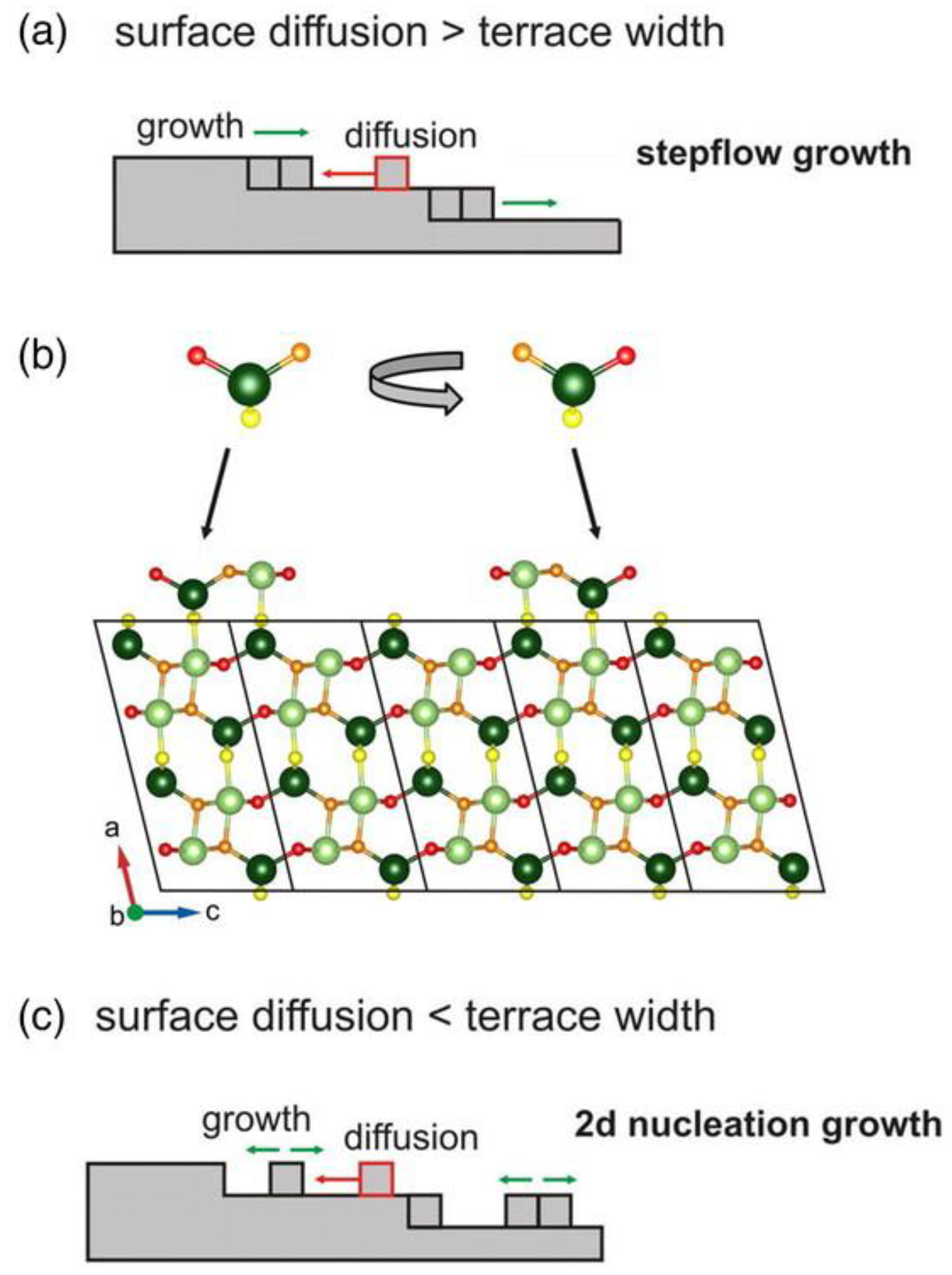
- Bin Anooz, S.; Grüneberg, R.; Wouters, C.; Schewski, R.; Albrecht, M.; Fiedler, A.; Irmscher, K.; Galazka, Z.; Miller, W.; Wagner, G.; et al. Step flow growth of β-Ga2O3 thin films on vicinal (100) β-Ga2O3 substrates grown by MOVPE. Appl. Phys. Lett. 2020, 116, 182106. [Google Scholar] [CrossRef]
- Schewski, R.; Lion, K.; Fiedler, A.; Wouters, C.; Popp, A.; Levchenko, S.V.; Schulz, T.; Schmidbauer, M.; Bin Anooz, S.; Grüneberg, R.; et al. Step-flow growth in homoepitaxy of β-Ga2O3 (100)—The influence of the miscut direction and faceting. APL Mater. 2019, 7, 022515. [Google Scholar] [CrossRef]
- Cheng, Z.; Hanke, M.; Galazka, Z.; Trampert, A. Growth mode evolution during (100)-oriented β-Ga2O3 homoepitaxy. Nanotechnology 2018, 29, 395705. [Google Scholar] [CrossRef]
- Ngo, T.S.; Le, D.D.; Lee, J.; Hong, S.-K.; Ha, J.-S.; Lee, W.-S.; Moon, Y.-B. Investigation of defect structure in homoepitaxial ((2)over-bar01) β-Ga2O3 layers prepared by plasma-assisted molecular beam epitaxy. J. Alloys Compd. 2020, 834, 155027. [Google Scholar] [CrossRef]
- Chou, T.-S.; Seyidov, P.; Bin Anooz, S.; Grüneberg, R.; Tran, T.T.V.; Irmscher, K.; Albrecht, M.; Galazka, Z.; Schwarzkopf, J.; Popp, A. Fast homoepitaxial growth of (100) β-Ga2O3 thin films via MOVPE. AIP Adv. 2021, 11, 115323. [Google Scholar] [CrossRef]
- Wang, D.; Ma, X.; Xiao, H.; Chen, R.; Le, Y.; Luan, C.; Zhang, B.; Ma, J. Effect of epitaxial growth rate on morphological, structural and optical properties of β-Ga2O3 films prepared by MOCVD. Mater. Res. Bull. 2022, 149, 111718. [Google Scholar] [CrossRef]
- Meng, L.; Yu, D.; Huang, H.-L.; Chae, C.; Hwang, J.; Zhao, H. MOCVD Growth of β-Ga2O3 on (001) Ga2O3 Substrates. Cryst. Growth Des. 2024, 24, 3737–3745. [Google Scholar] [CrossRef]
- Gottschalch, V.; Mergenthaler, K.; Wagner, G.; Bauer, J.; Paetzelt, H.; Sturm, C.; Teschner, U. Growth of β-Ga2O3 on Al2O3 and GaAs using metal-organic vapor-phase epitaxy. Phys. Status Solidi A 2009, 206, 243–249. [Google Scholar] [CrossRef]
- Gogova, D.; Wagner, G.; Baldini, M.; Schmidbauer, M.; Irmscher, K.; Schewski, R.; Galazka, Z.; Albrecht, M.; Fornari, R. Structural properties of Si-doped β-Ga2O3 layers grown by MOVPE. J. Cryst. Growth 2014, 401, 665–669. [Google Scholar] [CrossRef]
- Gogova, D.; Schmidbauer, M.; Kwasniewski, A. Homo- and heteroepitaxial growth of Sn-doped β-Ga2O3 layers by MOVPE. CrystEngComm 2015, 17, 6744–6752. [Google Scholar] [CrossRef]
- Kim, H.W.; Kim, N.H. Growth of gallium oxide thin films on silicon by the metal organic chemical vapor deposition method. Mater. Sci. Eng. B 2004, 110, 34–37. [Google Scholar] [CrossRef]
- Baldini, M.; Gogova, D.; Irmscher, K.; Schmidbauer, M.; Wagner, G.; Fornari, R. Heteroepitaxy of Ga2(1-x) In2xO3 layers by MOVPE with two different oxygen sources. Cryst. Res. Technol. 2014, 49, 552–557. [Google Scholar] [CrossRef]
- Song, Y.; Ranga, P.; Zhang, Y.; Feng, Z.; Huang, H.-L.; Santia, M.D.; Badescu, S.C.; Gonzalez-Valle, C.U.; Perez, C.; Ferri, K.; et al. Thermal Conductivity of β-Phase Ga2O3 and (AlxGa1–x)2O3 Heteroepitaxial Thin Films. ACS Appl. Mater. Interfaces 2021, 13, 38477–38490. [Google Scholar] [CrossRef]
- Chen, Y.; Liang, H.; Xia, X.; Tao, P.; Shen, R.; Liu, Y.; Feng, Y.; Zheng, Y.; Li, X.; Du, G. The lattice distortion of β-Ga2O3 film grown on c-plane sapphire. J. Mater. Sci. Mater. Electron. 2015, 26, 3231–3235. [Google Scholar] [CrossRef]
- Cao, Q.; He, L.; Xiao, H.; Feng, X.; Lv, Y.; Ma, J. β-Ga2O3 epitaxial films deposited on epi-GaN/sapphire (0001) substrates by MOCVD. Mater. Sci. Semicond. Process. 2018, 77, 58–63. [Google Scholar] [CrossRef]
- Wagner, G.; Baldini, M.; Gogova, D.; Schmidbauer, M.; Schewski, R.; Albrecht, M.; Galazka, Z.; Klimm, D.; Fornari, R. Homoepitaxial growth of β-Ga2O3 layers by metal-organic vapor phase epitaxy. Phys. Status Solidi A 2014, 211, 27–33. [Google Scholar] [CrossRef]
- Seo, D.; Kim, S.; Kim, H.-Y.; Jeon, D.-W.; Park, J.-H.; Hwang, W.S. Heteroepitaxial Growth of Single-Crystalline β-Ga2O3 on GaN/Al2O3 Using MOCVD. Cryst. Growth Des. 2023, 23, 7090–7094. [Google Scholar] [CrossRef]
- Tang, W.; Han, X.; Zhang, X.; Li, B.; Ma, Y.; Zhang, L.; Chen, T.; Zhou, X.; Bian, C.; Hu, Y.; et al. Homoepitaxial growth of (100) Si-doped β-Ga2O3 films via MOCVD. J. Semicond. 2023, 44, 062801. [Google Scholar] [CrossRef]
- Meng, L.; Bhuiyan, A.F.M.A.U.; Feng, Z.; Huang, H.-L.; Hwang, J.; Zhao, H. Metalorganic chemical vapor deposition of (100) β-Ga2O3 on on-axis Ga2O3 substrates. J. Vac. Sci. Technol. A 2022, 40, 062706. [Google Scholar] [CrossRef]
- Alema, F.; Zhang, Y.; Osinsky, A.; Orishchin, N.; Valente, N.; Mauze, A.; Speck, J.S. Low 114 cm−3 free carrier concentration in epitaxial β-Ga2O3 grown by MOCVD. APL Mater. 2020, 8, 021110. [Google Scholar] [CrossRef]
- Yue, J.; Ji, X.; Li, S.; Yan, Z.; Qi, X.; Li, P.; Tang, W. High thickness uniformity of 2-in. wafer-scale β-Ga2O3 films grown by MOCVD and photoelectrical properties. J. Vac. Sci. Technol. A 2022, 40, 062702. [Google Scholar] [CrossRef]
- Suzuki, N.; Ohira, S.; Tanaka, M.; Sugawara, T.; Nakajima, K.; Shishido, T. Fabrication and characterization of transparent conductive Sn-doped β-Ga2O3 single crystal. Phys. Status Solidi C 2007, 4, 2310–2313. [Google Scholar] [CrossRef]
- Ueda, N.; Hosono, H.; Waseda, R.; Kawazoe, H. Synthesis and control of conductivity of ultraviolet transmitting β-Ga2O3 single crystals. Appl. Phys. Lett. 1997, 70, 3561–3563. [Google Scholar] [CrossRef]
- Varley, J.B.; Weber, J.R.; Janotti, A.; Van De Walle, C.G. Oxygen vacancies and donor impurities in β-Ga2O3. Appl. Phys. Lett. 2010, 97, 142106. [Google Scholar] [CrossRef]
- Víllora, E.G.; Shimamura, K.; Yoshikawa, Y.; Ujiie, T.; Aoki, K. Electrical conductivity and carrier concentration control in β-Ga2O3 by Si doping. Appl. Phys. Lett. 2008, 92, 202120. [Google Scholar] [CrossRef]
- Zacherle, T.; Schmidt, P.C.; Martin, M. Ab initio calculations on the defect structure of β-Ga2O3. Phys. Rev. B 2013, 87, 235206. [Google Scholar] [CrossRef]
- Kyrtsos, A.; Matsubara, M.; Bellotti, E. Migration mechanisms and diffusion barriers of vacancies in Ga2O3. Phys. Rev. B 2017, 95, 245202. [Google Scholar] [CrossRef]
- Zhang, Y.; Speck, J.S. Importance of shallow hydrogenic dopants and material purity of ultra-wide bandgap semiconductors for vertical power electron devices. Semicond. Sci. Technol. 2020, 35, 125018. [Google Scholar] [CrossRef]
- Korhonen, E.; Tuomisto, F.; Gogova, D.; Wagner, G.; Baldini, M.; Galazka, Z.; Schewski, R.; Albrecht, M. Electrical compensation by Ga vacancies in Ga2O3 thin films. Appl. Phys. Lett. 2015, 106, 242103. [Google Scholar] [CrossRef]
- Zunger, A. Practical doping principles. Appl. Phys. Lett. 2003, 83, 57–59. [Google Scholar] [CrossRef]
- Lee, Y.-J.; Schweitz, M.A.; Lee, S.-K.; Koh, J.-H.; Koo, S.-M. Effect of Oxygen Annealing on the Characteristics of Isotype Ga2O3 /4H-SiC Heterojunction Diodes. J. Nanoelectron. Optoelectron. 2020, 15, 561–565. [Google Scholar] [CrossRef]
- Dong, L.; Jia, R.; Xin, B.; Zhang, Y. Effects of post-annealing temperature and oxygen concentration during sputtering on the structural and optical properties of β-Ga2O3 films. J. Vac. Sci. Technol. A 2016, 34, 060602. [Google Scholar] [CrossRef]
- Varley, J.B.; Janotti, A.; Franchini, C.; Van De Walle, C.G. Role of self-trapping in luminescence and p-type conductivity of wide-band-gap oxides. Phys. Rev. B 2012, 85, 081109. [Google Scholar] [CrossRef]
- Baldini, M.; Galazka, Z.; Wagner, G. Recent progress in the growth of β-Ga2O3 for power electronics applications. Mater. Sci. Semicond. Process. 2018, 78, 132–146. [Google Scholar] [CrossRef]
- Gil, E.; André, Y.; Cadoret, R.; Trassoudaine, A. Hydride Vapor Phase Epitaxy for Current III–V and Nitride Semiconductor Compound Issues. In Handbook of Crystal Growth; Elsevier: Amsterdam, The Netherlands, 2015; pp. 51–93. ISBN 978-0-444-63304-0. [Google Scholar]
- Fujito, K.; Kubo, S.; Nagaoka, H.; Mochizuki, T.; Namita, H.; Nagao, S. Bulk GaN crystals grown by HVPE. J. Cryst. Growth 2009, 311, 3011–3014. [Google Scholar] [CrossRef]
- Hu, J.; Wei, H.; Yang, S.; Li, C.; Li, H.; Liu, X.; Wang, L.; Wang, Z. Hydride vapor phase epitaxy for gallium nitride substrate. J. Semicond. 2019, 40, 101801. [Google Scholar] [CrossRef]
- Gil, E.; Andre, Y. Growth of long III-As NWs by hydride vapor phase epitaxy. Nanotechnology 2021, 32, 162002. [Google Scholar] [CrossRef]
- Dhanaraj, G.; Byrappa, K.; Prasad, V.; Dudley, M. Springer Handbook of Crystal Growth. Jpn. Mag. Mineral. Petrol. Sci. 2010, 39, 193a. [Google Scholar] [CrossRef]
- Xiu, X.; Zhang, L.; Li, Y.; Xiong, Z.; Zhang, R.; Zheng, Y. Application of halide vapor phase epitaxy for the growth of ultra-wide band gap Ga2O3. J. Semicond. 2019, 40, 011805. [Google Scholar] [CrossRef]
- Higashiwaki, M.; Fujita, S. Springer Series in Materials Science. In Gallium Oxide: Materials Properties, Crystal Growth, and Devices; Higashiwaki, M., Fujita, S., Eds.; Springer International Publishing: Berlin/Heidelberg, Germany, 2020; Volume 293, ISBN 978-3-030-37152-4. [Google Scholar]
- Nomura, K.; Goto, K.; Togashi, R.; Murakami, H.; Kumagai, Y.; Kuramata, A.; Yamakoshi, S.; Koukitu, A. Thermodynamic study of β-Ga2O3 growth by halide vapor phase epitaxy. J. Cryst. Growth 2014, 405, 19–22. [Google Scholar] [CrossRef]
- Oshima, Y.; Vίllora, E.G.; Shimamura, K. Quasi-heteroepitaxial growth of β-Ga2O3 on off-angled sapphire (0 0 0 1) substrates by halide vapor phase epitaxy. J. Cryst. Growth 2015, 410, 53–58. [Google Scholar] [CrossRef]
- Nikolaev, V.I.; Pechnikov, A.I.; Stepanov, S.I.; Nikitina, I.P.; Smirnov, A.N.; Chikiryaka, A.V.; Sharofidinov, S.S.; Bougrov, V.E.; Romanov, A.E. Epitaxial growth of (2¯01) β-Ga2O3 on (0001) sapphire substrates by halide vapour phase epitaxy. Mater. Sci. Semicond. Process. 2016, 47, 16–19. [Google Scholar] [CrossRef]
- Konishi, K.; Goto, K.; Togashi, R.; Murakami, H.; Higashiwaki, M.; Kuramata, A.; Yamakoshi, S.; Monemar, B.; Kumagai, Y. Comparison of O2 and H2O as oxygen source for homoepitaxial growth of β-Ga2O3 layers by halide vapor phase epitaxy. J. Cryst. Growth 2018, 492, 39–44. [Google Scholar] [CrossRef]
- Leach, J.H.; Udwary, K.; Rumsey, J.; Dodson, G.; Splawn, H.; Evans, K.R. Halide vapor phase epitaxial growth of β-Ga2O3 and α-Ga2O3 films. APL Mater. 2019, 7, 022504. [Google Scholar] [CrossRef]
- Xu, W.; Shi, J.; Li, Y.; Xiu, X.; Ding, S.; Xie, Z.; Tao, T.; Chen, P.; Liu, B.; Zhang, R.; et al. Study of β-Ga2O3 films hetero-epitaxially grown on off-angled sapphire substrates by halide vapor phase epitaxy. Mater. Lett. 2021, 289, 129411. [Google Scholar] [CrossRef]
- Nitta, K.; Sasaki, K.; Kuramata, A.; Murakami, H. Investigation of high speed β-Ga2O3 growth by solid-source trihalide vapor phase epitaxy. Jpn. J. Appl. Phys. 2023, 62, SF1021. [Google Scholar] [CrossRef]
- Oshima, Y.; Oshima, T. Homoepitaxial growth of 1ˉ02 β-Ga2O3 by halide vapor phase epitaxy. Semicond. Sci. Technol. 2023, 38, 105003. [Google Scholar] [CrossRef]
- Goto, K.; Murakami, H.; Kuramata, A.; Yamakoshi, S.; Higashiwaki, M.; Kumagai, Y. Effect of substrate orientation on homoepitaxial growth of β-Ga2O3 by halide vapor phase epitaxy. Appl. Phys. Lett. 2022, 120, 102102. [Google Scholar] [CrossRef]
- Sdoeung, S.; Sasaki, K.; Masuya, S.; Kawasaki, K.; Hirabayashi, J.; Kuramata, A.; Kasu, M. Stacking faults: Origin of leakage current in halide vapor phase epitaxial (001) β-Ga2O3 Schottky barrier diodes. Appl. Phys. Lett. 2021, 118, 172106. [Google Scholar] [CrossRef]
- Oshima, T.; Oshima, Y. Selective area growth of β-Ga2O3 by HCl-based halide vapor phase epitaxy. Appl. Phys. Express 2022, 15, 075503. [Google Scholar] [CrossRef]
- Roy, S.; Bhattacharyya, A.; Ranga, P.; Splawn, H.; Leach, J.; Krishnamoorthy, S. High-k Oxide Field-Plated Vertical (001) β-Ga2O3 Schottky Barrier Diode With Baliga’s Figure of Merit Over 1 GW/cm2. IEEE Electron Device Lett. 2021, 42, 1140–1143. [Google Scholar] [CrossRef]
- Li, W.; Hu, Z.; Nomoto, K.; Jinno, R.; Zhang, Z.; Tu, T.Q.; Sasaki, K.; Kuramata, A.; Jena, D.; Xing, H.G. 2.44 kV Ga2O3 vertical trench Schottky barrier diodes with very low reverse leakage current. In Proceedings of the 2018 IEEE International Electron Devices Meeting (IEDM), San Francisco, CA, USA, 1–5 December 2018; IEEE: Piscataway, NJ, USA, 2018; pp. 851–854. [Google Scholar]
- Dhara, S.; Kalarickal, N.K.; Dheenan, A.; Rahman, S.I.; Joishi, C.; Rajan, S. β-Ga2O3 trench Schottky diodes by low-damage Ga-atomic beam etching. Appl. Phys. Lett. 2023, 123, 023503. [Google Scholar] [CrossRef]
- Zhang, J.; Dong, P.; Dang, K.; Zhang, Y.; Yan, Q.; Xiang, H.; Su, J.; Liu, Z.; Si, M.; Gao, J.; et al. Ultra-wide bandgap semiconductor Ga2O3 power diodes. Nat. Commun. 2022, 13, 3900. [Google Scholar] [CrossRef]
- Gong, H.; Wang, Z.; Yu, X.; Ren, F.; Yang, Y.; Lv, Y.; Feng, Z.; Gu, S.; Zhang, R.; Zheng, Y.; et al. Field-Plated NiO/Ga2O3 p-n Heterojunction Power Diodes With High-Temperature Thermal Stability and Near Unity Ideality Factors. IEEE J. Electron Devices Soc. 2021, 9, 1166–1171. [Google Scholar] [CrossRef]
- Li, J.-S.; Wan, H.-H.; Chiang, C.-C.; Yoo, T.J.; Yu, M.-H.; Ren, F.; Kim, H.; Liao, Y.-T.; Pearton, S.J. Breakdown up to 13.5 kV in NiO/β-Ga2O3 Vertical Heterojunction Rectifiers. ECS J. Solid State Sci. Technol. 2024, 13, 035003. [Google Scholar] [CrossRef]
- Zhao, J.; Byggmästar, J.; He, H.; Nordlund, K.; Djurabekova, F.; Hua, M. Complex Ga2O3 polymorphs explored by accurate and general-purpose machine-learning interatomic potentials. Npj Comput. Mater. 2023, 9, 159. [Google Scholar] [CrossRef]
- Oshima, Y.; Víllora, E.G.; Shimamura, K. Halide vapor phase epitaxy of twin-free α-Ga2O3 on sapphire (0001) substrates. Appl. Phys. Express 2015, 8, 055501. [Google Scholar] [CrossRef]
- Oshima, Y.; Kawara, K.; Shinohe, T.; Hitora, T.; Kasu, M.; Fujita, S. Epitaxial lateral overgrowth of α-Ga2O3 by halide vapor phase epitaxy. APL Mater. 2019, 7, 022503. [Google Scholar] [CrossRef]
- Kawara, K.; Oshima, Y.; Okigawa, M.; Shinohe, T. Elimination of threading dislocations in α-Ga2O3 by double-layered epitaxial lateral overgrowth. Appl. Phys. Express 2020, 13, 075507. [Google Scholar] [CrossRef]
- Oshima, Y.; Víllora, E.G.; Matsushita, Y.; Yamamoto, S.; Shimamura, K. Epitaxial growth of phase-pure ε-Ga2O3 by halide vapor phase epitaxy. J. Appl. Phys. 2015, 118, 085301. [Google Scholar] [CrossRef]
- Oshima, Y.; Kawara, K.; Oshima, T.; Shinohe, T. In-plane orientation control of (001) κ-Ga2O3 by epitaxial lateral overgrowth through a geometrical natural selection mechanism. Jpn. J. Appl. Phys. 2020, 59, 115501. [Google Scholar] [CrossRef]
- Li, Y.; Xiu, X.; Xu, W.; Zhang, L.; Zhao, H.; Xie, Z.; Tao, T.; Chen, P.; Liu, B.; Zhang, R.; et al. Pure-phase κ-Ga2O3 layers grown on c-plane sapphire by halide vapor phase epitaxy. Superlattices Microstruct. 2021, 152, 106845. [Google Scholar] [CrossRef]
- Biswas, M.; Nishinaka, H. Thermodynamically metastable α-, ε- (or κ-), and γ-Ga2O3: From material growth to device applications. APL Mater. 2022, 10, 060701. [Google Scholar] [CrossRef]
- Tak, B.R.; Kumar, S.; Kapoor, A.K.; Wang, D.; Li, X.; Sun, H.; Singh, R. Recent advances in the growth of gallium oxide thin films employing various growth techniques—A review. J. Phys. Appl. Phys. 2021, 54, 453002. [Google Scholar] [CrossRef]
- Kawaharamura, T. Physics on development of open-air atmospheric pressure thin film fabrication technique using mist droplets: Control of precursor flow. Jpn. J. Appl. Phys. 2014, 53, 05FF08. [Google Scholar] [CrossRef]
- Kawaharamura, T.; Nishinaka, H.; Kamaka, Y.; Masuda, Y.; Lu, J.-G.; Fujita, S. Mist CVD Growth of ZnO-Based Thin Films and Nanostructures. J. Korean Phys. Soc. 2008, 53, 2976–2980. [Google Scholar] [CrossRef]
- Jeong, H.-J.; Kim, D.-H.; Park, J.; Park, J.-S. The impact of carrier gas on the physical and electrical properties of indium oxide layers grown by mist-CVD. Ceram. Int. 2018, 44, 6968–6972. [Google Scholar] [CrossRef]
- Yusa, S.; Oka, D.; Fukumura, T. High-κ dielectric ε-Ga2O3 stabilized in a transparent heteroepitaxial structure grown by mist CVD at atmospheric pressure. CrystEngComm 2020, 22, 381–385. [Google Scholar] [CrossRef]
- Park, S.-Y.; Ha, M.-T.; Kim, K.-H.; Van Lich, L.; Shin, Y.-J.; Jeong, S.-M.; Kwon, S.-H.; Bae, S.-Y. Enhanced thickness uniformity of large-scale α-Ga2O3 epilayers grown by vertical hot-wall mist chemical vapor deposition. Ceram. Int. 2022, 48, 5075–5082. [Google Scholar] [CrossRef]
- Uno, K.; Ohta, M.; Tanaka, I. Growth mechanism of α-Ga2O3 on a sapphire substrate by mist chemical vapor deposition using acetylacetonated gallium source solutions. Appl. Phys. Lett. 2020, 117, 052106. [Google Scholar] [CrossRef]
- Ha, M.; Kim, K.; Shin, Y.; Jeong, S.; Bae, S. Leidenfrost Motion of Water Microdroplets on Surface Substrate: Epitaxy of Gallium Oxide via Mist Chemical Vapor Deposition. Adv. Mater. Interfaces 2021, 8, 2001895. [Google Scholar] [CrossRef]
- Yan, P.; Zhang, Z.; Xu, Y.; Chen, H.; Chen, D.; Feng, Q.; Xu, S.; Zhang, Y.; Zhang, J.; Zhang, C.; et al. Heteroepitaxial growth and band alignment of β-Ga2O3 on GaN substrate grown by non-vacuum mist-CVD. Vacuum 2022, 204, 111381. [Google Scholar] [CrossRef]
- Cheng, Y.; Zhang, C.; Xu, Y.; Li, Z.; Chen, D.; Zhu, W.; Feng, Q.; Xu, S.; Zhang, J.; Hao, Y. Heteroepitaxial growth of β-Ga2O3 thin films on c-plane sapphire substrates with β-(AlxGa1-x)2O3 intermediate buffer layer by mist-CVD method. Mater. Today Commun. 2021, 29, 102766. [Google Scholar] [CrossRef]
- Xu, Y.; Zhang, C.; Yan, P.; Li, Z.; Zhang, Y.; Chen, D.; Zhu, W.; Feng, Q.; Xu, S.; Zhang, J.; et al. β-Ga2O3 epitaxial growth on Fe-GaN template by non-vacuum mist CVD and its application in Schottky barrier diodes. AIP Adv. 2021, 11, 075312. [Google Scholar] [CrossRef]
- Nishinaka, H.; Nagaoka, T.; Kajita, Y.; Yoshimoto, M. Rapid homoepitaxial growth of (010) β-Ga2O3 thin films via mist chemical vapor deposition. Mater. Sci. Semicond. Process. 2021, 128, 105732. [Google Scholar] [CrossRef]
- Lee, S.; Kaneko, K.; Fujita, S. Homoepitaxial growth of beta gallium oxide films by mist chemical vapor deposition. Jpn. J. Appl. Phys. 2016, 55, 1202B8. [Google Scholar] [CrossRef]
- Ogawa, T.; Nishinaka, H.; Shimazoe, K.; Nagaoka, T.; Miyake, H.; Kanegae, K.; Yoshimoto, M. Homoepitaxial growth of Ge doped β-gallium oxide thin films by mist chemical vapor deposition. Jpn. J. Appl. Phys. 2023, 62, SF1016. [Google Scholar] [CrossRef]
- Hosaka, S.; Nishinaka, H.; Ogawa, T.; Miyake, H.; Yoshimoto, M. High conductivity of n-type β-Ga2O3(010) thin films achieved through Si doping by mist chemical vapor deposition. AIP Adv. 2024, 14, 015040. [Google Scholar] [CrossRef]
- Takane, H.; Ando, Y.; Takahashi, H.; Makisako, R.; Ikeda, H.; Ueda, T.; Suda, J.; Tanaka, K.; Fujita, S.; Sugaya, H. Prospects of mist CVD for fabrication of β-Ga2O3 MESFETs on β-Ga2O3 (010) substrates. Appl. Phys. Express 2023, 16, 081004. [Google Scholar] [CrossRef]
- An, Y.; Dai, L.; Wu, Y.; Wu, B.; Zhao, Y.; Liu, T.; Hao, H.; Li, Z.; Niu, G.; Zhang, J.; et al. Epitaxial growth of β-Ga2O3 thin films on Ga2O3 and Al2O3 substrates by using pulsed laser deposition. J. Adv. Dielectr. 2019, 9, 1950032. [Google Scholar] [CrossRef]
- Wang, C.; Li, S.-W.; Fan, W.-H.; Zhang, Y.-C.; Zhang, X.-Y.; Guo, R.-R.; Lin, H.-J.; Lien, S.-Y.; Zhu, W.-Z. Structural, optical and morphological evolution of Ga2O3/Al2O3 (0001) films grown at various temperatures by pulsed laser deposition. Ceram. Int. 2021, 47, 29748–29757. [Google Scholar] [CrossRef]
- Wu, Y.; Yan, X.; Jiang, Y.; Yao, T.; Chen, C.; Ye, H. Microstructure and optical properties of β-Ga2O3 thin films fabricated by pulsed laser deposition. Thin Solid Films 2024, 796, 140336. [Google Scholar] [CrossRef]
- Shepelin, N.A.; Tehrani, Z.P.; Ohannessian, N.; Schneider, C.W.; Pergolesi, D.; Lippert, T. A practical guide to pulsed laser deposition. Chem. Soc. Rev. 2023, 52, 2294–2321. [Google Scholar] [CrossRef]
- Shen, H.; Baskaran, K.; Yin, Y.; Tian, K.; Duan, L.; Zhao, X.; Tiwari, A. Effect of thickness on the performance of solar blind photodetectors fabricated using PLD grown β-Ga2O3 thin films. J. Alloys Compd. 2020, 822, 153419. [Google Scholar] [CrossRef]
- Khartsev, S.; Hammar, M.; Nordell, N.; Zolotarjovs, A.; Purans, J.; Hallén, A. Reverse-Bias Electroluminescence in Er-Doped β-Ga2O3 Schottky Barrier Diodes Manufactured by Pulsed Laser Deposition. Phys. Status Solidi A 2022, 219, 2100610. [Google Scholar] [CrossRef]
- Leedy, K.D.; Chabak, K.D.; Vasilyev, V.; Look, D.C.; Boeckl, J.J.; Brown, J.L.; Tetlak, S.E.; Green, A.J.; Moser, N.A.; Crespo, A.; et al. Highly conductive homoepitaxial Si-doped Ga2O3 films on (010) β-Ga2O3 by pulsed laser deposition. Appl. Phys. Lett. 2017, 111, 012103. [Google Scholar] [CrossRef]
- Bruni, F.J. Crystal growth of sapphire for substrates for high-brightness, light emitting diodes. Cryst. Res. Technol. 2015, 50, 133–142. [Google Scholar] [CrossRef]
- Yang, H.; Qian, Y.; Zhang, C.; Wuu, D.-S.; Talwar, D.N.; Lin, H.-H.; Lee, J.-F.; Wan, L.; He, K.; Feng, Z.C. Surface/structural characteristics and band alignments of thin Ga2O3 films grown on sapphire by pulse laser deposition. Appl. Surf. Sci. 2019, 479, 1246–1253. [Google Scholar] [CrossRef]
- Hu, C.; Zhang, F.; Saito, K.; Tanaka, T.; Guo, Q. Low temperature growth of Ga2O3 films on sapphire substrates by plasma assisted pulsed laser deposition. AIP Adv. 2019, 9, 085022. [Google Scholar] [CrossRef]
- Wakabayashi, R.; Yoshimatsu, K.; Hattori, M.; Ohtomo, A. Epitaxial structure and electronic property of β-Ga2O3 films grown on MgO (100) substrates by pulsed-laser deposition. Appl. Phys. Lett. 2017, 111, 162101. [Google Scholar] [CrossRef]
- Berencén, Y.; Xie, Y.; Wang, M.; Prucnal, S.; Rebohle, L.; Zhou, S. Structural and optical properties of pulsed-laser deposited crystalline β-Ga2O3 thin films on silicon. Semicond. Sci. Technol. 2019, 34, 035001. [Google Scholar] [CrossRef]
- Zade, V.; Makeswaran, N.; Boyce, B.L.; Paraguay-Delgado, F.; Ramana, C.V. Structural and mechanical properties of nanocrystalline Ga2O3 films made by pulsed laser deposition onto transparent quartz substrates. Nano Express 2021, 2, 020006. [Google Scholar] [CrossRef]
- Yang, H.; Liu, Y.; Luo, X.; Li, Y.; Wuu, D.-S.; He, K.; Feng, Z.C. Effects of growth temperature and thickness on structure and optical properties of Ga2O3 films grown by pulsed laser deposition. Superlattices Microstruct. 2019, 131, 21–29. [Google Scholar] [CrossRef]
- Oanh Vu, T.K.; Lee, D.U.; Kim, E.K. The effect of oxygen partial pressure on band gap modulation of Ga2O3 grown by pulsed laser deposition. J. Alloys Compd. 2019, 806, 874–880. [Google Scholar] [CrossRef]
- Blumenschein, N.; Paskova, T.; Muth, J.F. Effect of Growth Pressure on PLD-Deposited Gallium Oxide Thin Films for Deep-UV Photodetectors. Phys. Status Solidi A 2019, 216, 1900098. [Google Scholar] [CrossRef]
- Leedy, K.D.; Chabak, K.D.; Vasilyev, V.; Look, D.C.; Mahalingam, K.; Brown, J.L.; Green, A.J.; Bowers, C.T.; Crespo, A.; Thomson, D.B.; et al. Si content variation and influence of deposition atmosphere in homoepitaxial Si-doped β-Ga2O3 films by pulsed laser deposition. APL Mater. 2018, 6, 101102. [Google Scholar] [CrossRef]
- Zheng, T.; He, W.; Wang, L.; Li, J.; Zheng, S. Effect of different substrates on Si and Ta co-doped Ga2O3 films prepared by pulsed laser deposition. J. Cryst. Growth 2020, 533, 125455. [Google Scholar] [CrossRef]
- Kim, T.; Kim, Y.; Jeong, W.C.; Jeong, M.S.; Kim, E.K. Effect of Oxygen Plasma on β-Ga2O3 Deep Ultraviolet Photodetectors Fabricated by Plasma-Assisted Pulsed Laser Deposition. ACS Appl. Electron. Mater. 2023, 5, 2590–2597. [Google Scholar] [CrossRef]
- Yang, Z.; Hao, J. Progress in pulsed laser deposited two-dimensional layered materials for device applications. J. Mater. Chem. C 2016, 4, 8859–8878. [Google Scholar] [CrossRef]
- Ashfold, M.N.R.; Claeyssens, F.; Fuge, G.M.; Henley, S.J. Pulsed laser ablation and deposition of thin films. Chem. Soc. Rev. 2004, 33, 23. [Google Scholar] [CrossRef] [PubMed]
- Rafique, S.; Han, L.; Zhao, H. Synthesis of wide bandgap Ga2O3 (Eg ∼4.6-4.7 eV) thin films on sapphire by low pressure chemical vapor deposition: Synthesis of wide bandgap Ga2O3 thin films on sapphire. Phys. Status Solidi A 2016, 213, 1002–1009. [Google Scholar] [CrossRef]
- Joshi, G.; Chauhan, Y.S.; Verma, A. Temperature dependence of β-Ga2O3 heteroepitaxy on c-plane sapphire using low pressure chemical vapor deposition. J. Alloys Compd. 2021, 883, 160799. [Google Scholar] [CrossRef]
- Ghadi, H.; McGlone, J.F.; Cornuelle, E.; Feng, Z.; Zhang, Y.; Meng, L.; Zhao, H.; Arehart, A.R.; Ringel, S.A. Deep level defects in low-pressure chemical vapor deposition grown (010) β-Ga2O3. APL Mater. 2022, 10, 101110. [Google Scholar] [CrossRef]
- Ghadi, H.; McGlone, J.F.; Jackson, C.M.; Farzana, E.; Feng, Z.; Bhuiyan, A.F.M.A.U.; Zhao, H.; Arehart, A.R.; Ringel, S.A. Full bandgap defect state characterization of β-Ga2O3 grown by metal organic chemical vapor deposition. APL Mater. 2020, 8, 021111. [Google Scholar] [CrossRef]
- Ghadi, H.; McGlone, J.F.; Feng, Z.; Bhuiyan, A.F.M.A.U.; Zhao, H.; Arehart, A.R.; Ringel, S.A. Influence of growth temperature on defect states throughout the bandgap of MOCVD-grown β-Ga2O3. Appl. Phys. Lett. 2020, 117, 172106. [Google Scholar] [CrossRef]
- Rafique, S.; Han, L.; Neal, A.T.; Mou, S.; Tadjer, M.J.; French, R.H.; Zhao, H. Heteroepitaxy of N-type β-Ga2O3 thin films on sapphire substrate by low pressure chemical vapor deposition. Appl. Phys. Lett. 2016, 109, 132103. [Google Scholar] [CrossRef]
- Joshi, G.; Chauhan, Y.S.; Verma, A. Investigation of growth dynamics of β-Ga2O3 LPCVD by independently controlling Ga precursor and substrate temperature. Jpn. J. Appl. Phys. 2023, 62, SF1017. [Google Scholar] [CrossRef]
- Rafique, S.; Han, L.; Mou, S.; Zhao, H. Temperature and doping concentration dependence of the energy band gap in β-Ga2O3 thin films grown on sapphire. Opt. Mater. Express 2017, 7, 3561. [Google Scholar] [CrossRef]
- Xu, B.; Hu, J.; He, X.; Wang, X.; Li, D.; Chen, C. Effect of Growth Temperature on the Characteristics of β-Ga203 Thin Films Grown on 4H-SiC (0001) Substrates by Low Pressure Chemical Vapor Deposition. In Proceedings of the 2021 IEEE 4th International Conference on Electronics Technology (ICET), Chengdu, China, 7–10 May 2021; IEEE: Piscataway, NJ, USA, 2021; pp. 5–8. [Google Scholar]
- Saquib, T.; Akyol, F.; Ozden, H.; Somaiah, N.; Sahoo, J.; Muralidharan, R.; Nath, D.N. Carrier transport in LPCVD grown Ge-doped β-Ga2O3/4H-SiC isotype heterojunction. J. Appl. Phys. 2024, 135, 065701. [Google Scholar] [CrossRef]
- Karim, M.R.; Chen, Z.; Feng, Z.; Huang, H.-L.; Johnson, J.M.; Tadjer, M.J.; Hwang, J.; Zhao, H. Two-step growth of β-Ga2O3 films on (100) diamond via low pressure chemical vapor deposition. J. Vac. Sci. Technol. Vac. Surf. Films 2021, 39, 023411. [Google Scholar] [CrossRef]
- Vogt, P.; Bierwagen, O. Reaction kinetics and growth window for plasma-assisted molecular beam epitaxy of Ga2O3: Incorporation of Ga vs. Ga2O desorption. Appl. Phys. Lett. 2016, 108, 072101. [Google Scholar] [CrossRef]
- Joishi, C.; Rafique, S.; Xia, Z.; Han, L.; Krishnamoorthy, S.; Zhang, Y.; Lodha, S.; Zhao, H.; Rajan, S. Low-pressure CVD-grown β-Ga2O3 bevel-field-plated Schottky barrier diodes. Appl. Phys. Express 2018, 11, 031101. [Google Scholar] [CrossRef]
- Saha, S.; Meng, L.; Feng, Z.; Anhar Uddin Bhuiyan, A.F.M.; Zhao, H.; Singisetti, U. Schottky diode characteristics on high-growth rate LPCVD β-Ga2O3 films on (010) and (001) Ga2O3 substrates. Appl. Phys. Lett. 2022, 120, 122106. [Google Scholar] [CrossRef]
- Mondal, A.; Nandi, S.; Yadav, M.K.; Nandi, A.; Bag, A. Broad Range (254–302 nm) and High Performance Ga2O3: SnO2 Based Deep UV Photodetector. IEEE Trans. Nanotechnol. 2022, 21, 320–327. [Google Scholar] [CrossRef]
- Rafique, S.; Han, L.; Zhao, H. Thermal annealing effect on β-Ga2O3 thin film solar blind photodetector heteroepitaxially grown on sapphire substrate: Thermal annealing effect on β-Ga2O3 thin film solar blind photodetector. Phys. Status Solidi A 2017, 214, 1700063. [Google Scholar] [CrossRef]
- Lin, Z.; Zhang, J.; Xu, S.; Chen, Z.; Yang, S.; Tian, K.; Su, X.; Shi, X.; Hao, Y. Influence of vicinal sapphire substrate on the properties of N-polar GaN films grown by metal-organic chemical vapor deposition. Appl. Phys. Lett. 2014, 105, 082114. [Google Scholar] [CrossRef]
- Shen, X.Q.; Matsuhata, H.; Okumura, H. Reduction of the threading dislocation density in GaN films grown on vicinal sapphire (0001) substrates. Appl. Phys. Lett. 2005, 86, 021912. [Google Scholar] [CrossRef]
- Rafique, S.; Han, L.; Neal, A.T.; Mou, S.; Boeckl, J.; Zhao, H. Towards High-Mobility Heteroepitaxial β-Ga2O3 on Sapphire−Dependence on The Substrate Off-Axis Angle. Phys. Status Solidi A 2018, 215, 1700467. [Google Scholar] [CrossRef]
- Feng, Z.; Karim, M.R.; Zhao, H. Low pressure chemical vapor deposition of β-Ga2O3 thin films: Dependence on growth parameters. APL Mater. 2019, 7, 022514. [Google Scholar] [CrossRef]
- Akyol, F.; Demir, İ. Close oxygen coupled low-pressure chemical vapor deposition growth of high quality β-Ga2O3 on sapphire. Mater. Sci. Semicond. Process. 2022, 146, 106645. [Google Scholar] [CrossRef]
- Zhang, Y.; Feng, Z.; Karim, M.R.; Zhao, H. High-temperature low-pressure chemical vapor deposition of β-Ga2O3. J. Vac. Sci. Technol. Vac. Surf. Films 2020, 38, 050806. [Google Scholar] [CrossRef]
- Wu, S.; Liu, Z.; Yang, H.; Wang, Y. The effects of high temperature thermal treatments on β-Ga2O3 films grown on c-sapphire by low-pressure CVD. J. Phys. Appl. Phys. 2024, 57, 015104. [Google Scholar] [CrossRef]
- Xu, B.; Hu, J.; Meng, J.; He, X.; Wang, X.; Pu, H. Study of the Bonding Characteristics at β-Ga2O3(201)/4H-SiC (0001) Interfaces from First Principles and Experiment. Crystals 2023, 13, 160. [Google Scholar] [CrossRef]
- Akyol, F.; Ozden, H. Chemical vapor deposition growth of β-Ga2O3 on Si- and C- face off-axis 4H-SiC at high temperature. Mater. Sci. Semicond. Process. 2024, 170, 107968. [Google Scholar] [CrossRef]
- Hu, J.; Xu, B.; Zhang, Z.; He, X.; Li, L.; Cheng, H.; Wang, J.; Meng, J.; Wang, X.; Zhang, C.; et al. Step flow growth of β-Ga2O3 films on off-axis 4H-SiC substrates by LPCVD. Surf. Interfaces 2023, 37, 102732. [Google Scholar] [CrossRef]
- Rafique, S.; Han, L.; Tadjer, M.J.; Freitas, J.A.; Mahadik, N.A.; Zhao, H. Homoepitaxial growth of β-Ga2O3 thin films by low pressure chemical vapor deposition. Appl. Phys. Lett. 2016, 108, 182105. [Google Scholar] [CrossRef]
- Rafique, S.; Karim, M.R.; Johnson, J.M.; Hwang, J.; Zhao, H. LPCVD homoepitaxy of Si doped β-Ga2O3 thin films on (010) and (001) substrates. Appl. Phys. Lett. 2018, 112, 052104. [Google Scholar] [CrossRef]
- Ahmadi, E.; Koksaldi, O.S.; Kaun, S.W.; Oshima, Y.; Short, D.B.; Mishra, U.K.; Speck, J.S. Ge doping of β-Ga2O3 films grown by plasma-assisted molecular beam epitaxy. Appl. Phys. Express 2017, 10, 041102. [Google Scholar] [CrossRef]
- Mondal, A.; Yadav, M.K.; Bag, A. Transition from thin film to nanostructure in low pressure chemical vapor deposition growth of β-Ga2O3: Impact of metal gallium source. Thin Solid Films 2020, 709, 138234. [Google Scholar] [CrossRef]
- Tang, M.; Wang, G.; Wu, S.; Xiang, Y. One-Step Preparation of Si-Doped Ultra-Long β-Ga2O3 Nanowires by Low-Pressure Chemical Vapor Deposition. Crystals 2023, 13, 898. [Google Scholar] [CrossRef]
- Han, N.; Wang, F.; Yang, Z.; Yip, S.; Dong, G.; Lin, H.; Fang, M.; Hung, T.; Ho, J.C. Low-temperature growth of highly crystalline β-Ga2O3 nanowires by solid-source chemical vapor deposition. Nanoscale Res. Lett. 2014, 9, 347. [Google Scholar] [CrossRef]
- López, I.; Castaldini, A.; Cavallini, A.; Nogales, E.; Méndez, B.; Piqueras, J. β-Ga2O3 nanowires for an ultraviolet light selective frequency photodetector. J. Phys. Appl. Phys. 2014, 47, 415101. [Google Scholar] [CrossRef]
- Tian, W.; Zhi, C.; Zhai, T.; Chen, S.; Wang, X.; Liao, M.; Golberg, D.; Bando, Y. In-doped Ga2O3 nanobelt based photodetector with high sensitivity and wide-range photoresponse. J. Mater. Chem. 2012, 22, 17984. [Google Scholar] [CrossRef]
- Zhong, M.; Wei, Z.; Meng, X.; Wu, F.; Li, J. High-performance single crystalline UV photodetectors of β-Ga2O3. J. Alloys Compd. 2015, 619, 572–575. [Google Scholar] [CrossRef]
- Hsieh, C.-H.; Chou, L.-J.; Lin, G.-R.; Bando, Y.; Golberg, D. Nanophotonic Switch: Gold-in-Ga2O3 Peapod Nanowires. Nano Lett. 2008, 8, 3081–3085. [Google Scholar] [CrossRef]
- Kim, H.; Jin, C.; An, S.; Lee, C. Fabrication and CO gas-sensing properties of Pt-functionalized Ga2O3 nanowires. Ceram. Int. 2012, 38, 3563–3567. [Google Scholar] [CrossRef]
- Chang, P.-C.; Fan, Z.; Tseng, W.-Y.; Rajagopal, A.; Lu, J.G. β-Ga2O3 nanowires: Synthesis, characterization, and p-channel field-effect transistor. Appl. Phys. Lett. 2005, 87, 222102. [Google Scholar] [CrossRef]
- Wu, Y.-L.; Luan, Q.; Chang, S.-J.; Jiao, Z.; Weng, W.Y.; Lin, Y.-H.; Hsu, C.L. Highly Sensitive β-Ga2O3 Nanowire Nanowires Isopropyl Alcohol Sensor. IEEE Sens. J. 2014, 14, 401–405. [Google Scholar] [CrossRef]
- Huang, Y.; Yue, S.; Wang, Z.; Wang, Q.; Shi, C.; Xu, Z.; Bai, X.D.; Tang, C.; Gu, C. Preparation and Electrical Properties of Ultrafine Ga2O3 Nanowires. J. Phys. Chem. B 2006, 110, 796–800. [Google Scholar] [CrossRef] [PubMed]
- Mazeina, L.; Bermudez, V.M.; Perkins, F.K.; Arnold, S.P.; Prokes, S.M. Interaction of functionalized Ga2O3 NW-based room temperature gas sensors with different hydrocarbons. Sens. Actuators B Chem. 2010, 151, 114–120. [Google Scholar] [CrossRef]
- Vanithakumari, S.C.; Nanda, K.K. A One-Step Method for the Growth of Ga2O3-Nanorod-Based White-Light-Emitting Phosphors. Adv. Mater. 2009, 21, 3581–3584. [Google Scholar] [CrossRef]
- Wang, Y.; Li, N.; Duan, P.; Sun, X.; Chu, B.; He, Q. Properties and Photocatalytic Activity of β-Ga2O3 Nanorods under Simulated Solar Irradiation. J. Nanomater. 2015, 2015, 1–5. [Google Scholar] [CrossRef]
- Zhao, B.; Li, X.; Yang, L.; Wang, F.; Li, J.; Xia, W.; Li, W.; Zhou, L.; Zhao, C. β-Ga2O3 Nanorod Synthesis with a One-step Microwave Irradiation Hydrothermal Method and its Efficient Photocatalytic Degradation for Perfluorooctanoic Acid. Photochem. Photobiol. 2015, 91, 42–47. [Google Scholar] [CrossRef] [PubMed]
- Gai, L.; Jiang, H.; Tian, Y.; Cui, D.; Wang, Q. Low-temperature synthesis of β-Ga2O3 nanorods on SBA-15 microparticles by solvothermal method. Nanotechnology 2006, 17, 5858–5861. [Google Scholar] [CrossRef]
- Zhao, W.; Yang, Y.; Hao, R.; Liu, F.; Wang, Y.; Tan, M.; Tang, J.; Ren, D.; Zhao, D. Synthesis of mesoporous β-Ga2O3 nanorods using PEG as template: Preparation, characterization and photocatalytic properties. J. Hazard. Mater. 2011, 192, 1548–1554. [Google Scholar] [CrossRef]
- Zheng, X.-Q.; Lee, J.; Rafique, S.; Zhao, H.; Feng, P.X.-L. Towards Real-Time Middle Ultraviolet (MUV) Light Detection by Beta Gallium OXIDE (β-Ga2O3) Nems Oscillator. In Proceedings of the 2018 Solid-State, Actuators, and Microsystems Workshop Technical Digest, Hilton Head, SC, USA, 3–7 June 2018; Transducer Research Foundation: San Diego, CA, USA, 2018; pp. 92–93. [Google Scholar]
- Zheng, X.-Q.; Lee, J.; Rafique, S.; Han, L.; Zorman, C.A.; Zhao, H.; Feng, P.X.-L. Ultrawide Band Gap β-Ga2O3 Nanomechanical Resonators with Spatially Visualized Multimode Motion. ACS Appl. Mater. Interfaces 2017, 9, 43090–43097. [Google Scholar] [CrossRef]
- Jiao, Y.; Jiang, Q.; Meng, J.; Zhao, J.; Yin, Z.; Gao, H.; Zhang, J.; Deng, J.; Zhang, X. Growth and characteristics of β-Ga2O3 thin films on sapphire (0001) by low pressure chemical vapour deposition. Vacuum 2021, 189, 110253. [Google Scholar] [CrossRef]
- Ranga, P.; Bhattacharyya, A.; Whittaker-Brooks, L.; Scarpulla, M.A.; Krishnamoorthy, S. N-type doping of low-pressure chemical vapor deposition grown β-Ga2O3 thin films using solid-source germanium. J. Vac. Sci. Technol. Vac. Surf. Films 2021, 39, 030404. [Google Scholar] [CrossRef]
- Mahmoodinezhad, A.; Janowitz, C.; Naumann, F.; Plate, P.; Gargouri, H.; Henkel, K.; Schmeiβer, D.; Flege, J.I. Low-temperature growth of gallium oxide thin films by plasma-enhanced atomic layer deposition. J. Vac. Sci. Technol. Vac. Surf. Films 2020, 38, 022404. [Google Scholar] [CrossRef]
- Sbrockey, N.M.; Salagaj, T.; Coleman, E.; Tompa, G.S.; Moon, Y.; Kim, M.S. Large-Area MOCVD Growth of Ga2O3 in a Rotating Disc Reactor. J. Electron. Mater. 2015, 44, 1357–1360. [Google Scholar] [CrossRef]
- Hao, J.G.; Ma, T.C.; Chen, X.H.; Kuang, Y.; Li, L.; Li, J.; Ren, F.-F.; Gu, S.L.; Tan, H.H.; Jagadish, C.; et al. Phase tailoring and wafer-scale uniform hetero-epitaxy of metastable-phased corundum α-Ga2O3 on sapphire. Appl. Surf. Sci. 2020, 513, 145871. [Google Scholar] [CrossRef]
- Kim, S.; Kim, H.W.; Kim, H.-Y.; Jeon, D.-W.; Cho, S.B.; Park, J.-H. A pre-reaction suppressing strategy for α-Ga2O3 halide vapor pressure epitaxy using asymmetric precursor gas flow. CrystEngComm 2022, 24, 3049–3056. [Google Scholar] [CrossRef]

Disclaimer/Publisher’s Note: The statements, opinions and data contained in all publications are solely those of the individual author(s) and contributor(s) and not of MDPI and/or the editor(s). MDPI and/or the editor(s) disclaim responsibility for any injury to people or property resulting from any ideas, methods, instructions or products referred to in the content. |
© 2024 by the authors. Licensee MDPI, Basel, Switzerland. This article is an open access article distributed under the terms and conditions of the Creative Commons Attribution (CC BY) license (https://creativecommons.org/licenses/by/4.0/).
Share and Cite
Rahaman, I.; Ellis, H.D.; Chang, C.; Mudiyanselage, D.H.; Xu, M.; Da, B.; Fu, H.; Zhao, Y.; Fu, K. Epitaxial Growth of Ga2O3: A Review. Materials 2024, 17, 4261. https://doi.org/10.3390/ma17174261
Rahaman I, Ellis HD, Chang C, Mudiyanselage DH, Xu M, Da B, Fu H, Zhao Y, Fu K. Epitaxial Growth of Ga2O3: A Review. Materials. 2024; 17(17):4261. https://doi.org/10.3390/ma17174261
Chicago/Turabian StyleRahaman, Imteaz, Hunter D. Ellis, Cheng Chang, Dinusha Herath Mudiyanselage, Mingfei Xu, Bingcheng Da, Houqiang Fu, Yuji Zhao, and Kai Fu. 2024. "Epitaxial Growth of Ga2O3: A Review" Materials 17, no. 17: 4261. https://doi.org/10.3390/ma17174261
APA StyleRahaman, I., Ellis, H. D., Chang, C., Mudiyanselage, D. H., Xu, M., Da, B., Fu, H., Zhao, Y., & Fu, K. (2024). Epitaxial Growth of Ga2O3: A Review. Materials, 17(17), 4261. https://doi.org/10.3390/ma17174261