
Thermal and Mechanical Properties of Amorphous Silicon Carbide Thin Films Using the Femtosecond Pump-Probe Technique


Abstract
:1. Introduction
2. Materials and Methods
2.1. Experimental
2.2. Theory and Computation
3. Results
3.1. Sample Characteristics
3.2. Femtosecond Pump-Probe Experiment Results
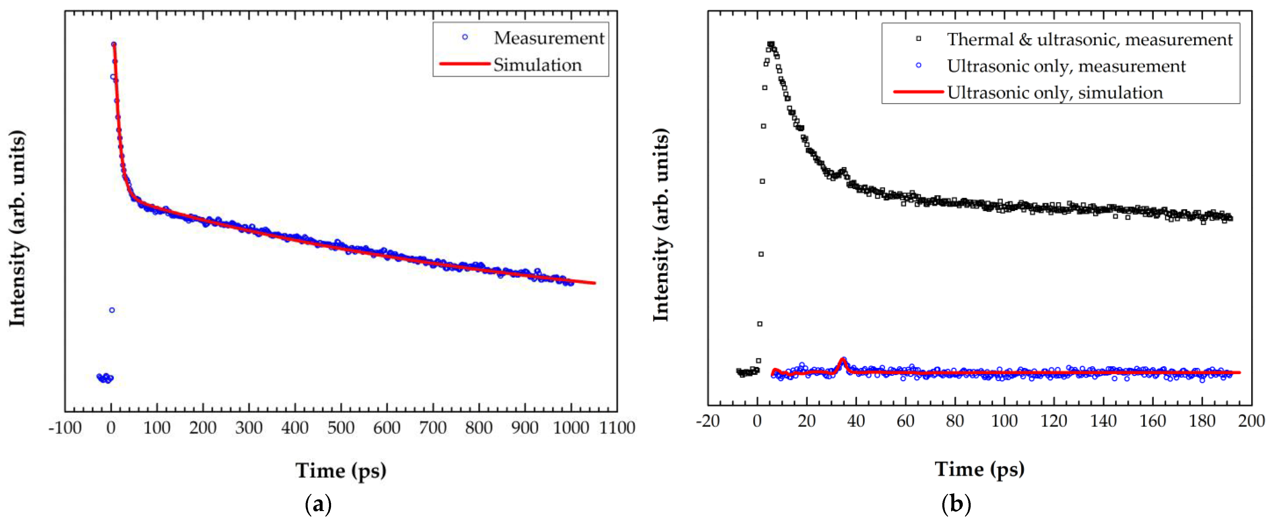
3.2.1. Al Film
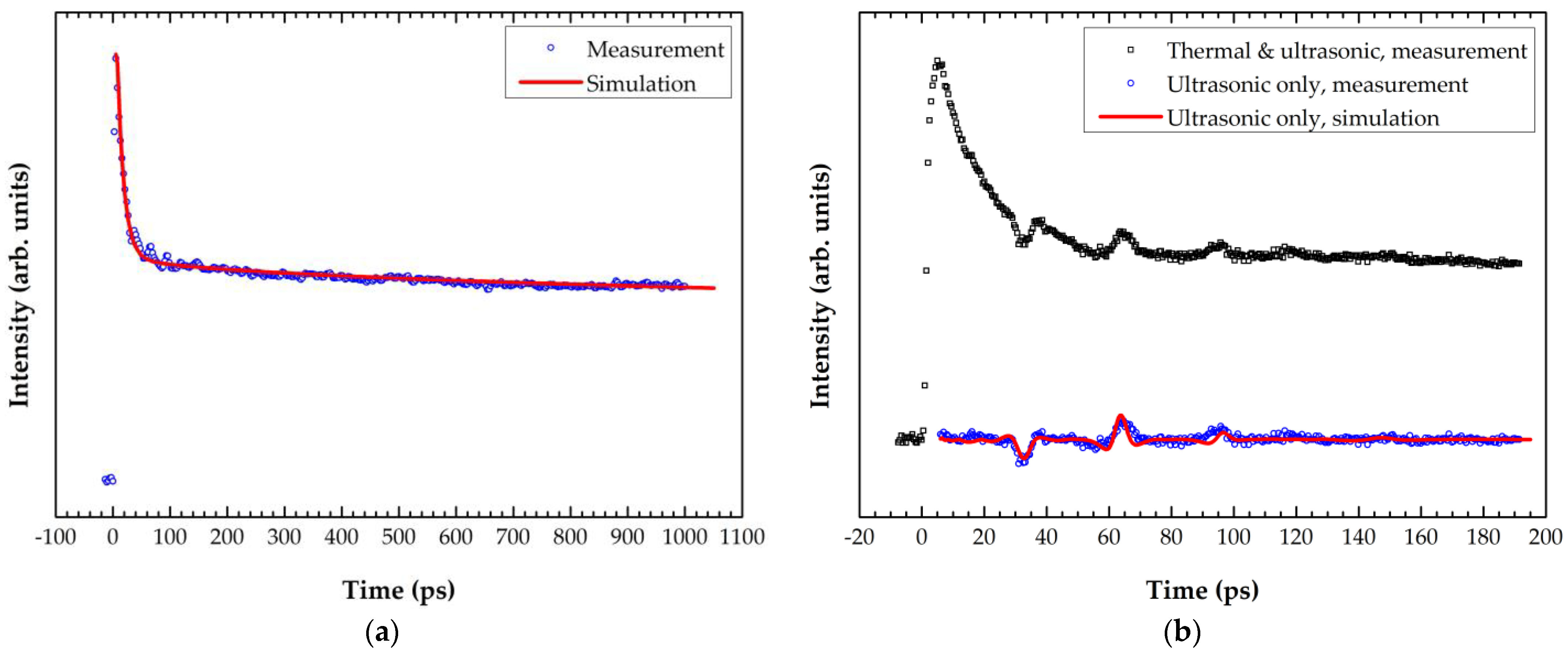
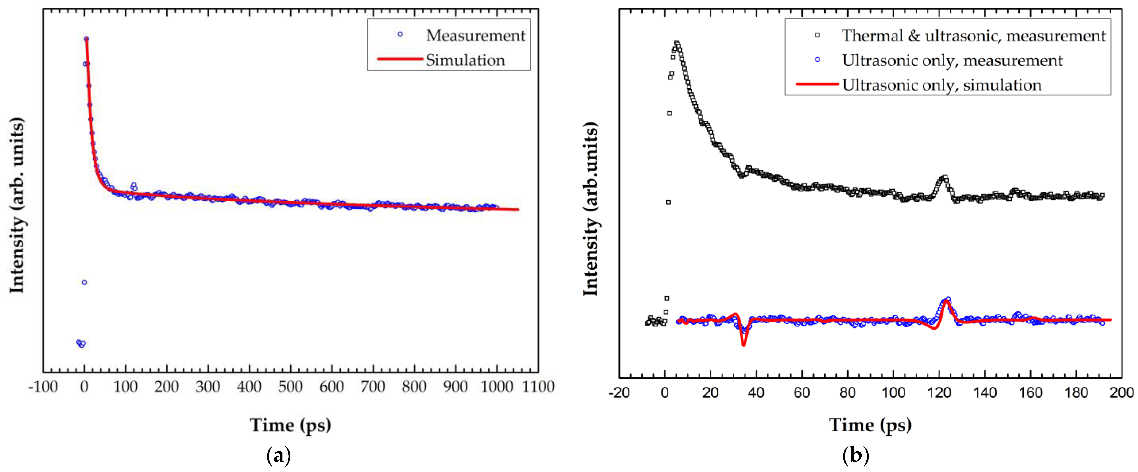
3.2.2. a-SiC Films
4. Discussion
5. Conclusions
Funding
Institutional Review Board Statement
Informed Consent Statement
Data Availability Statement
Acknowledgments
Conflicts of Interest
References
- Fraga, M.; Pessoa, R. Progresses in synthesis and application of SiC films: From CVD to ALD and from MEMS to NEMS. Micromachines 2020, 11, 799. [Google Scholar] [CrossRef] [PubMed]
- Wingert, M.C.; Zheng, J.; Kwon, S.; Chen, R. Thermal transport in amorphous materials: A review. Semicond. Sci. Technol. 2016, 31, 113003. [Google Scholar] [CrossRef]
- Sarro, P.M. Silicon carbide as a new MEMS technology. Sens. Actuators A Phys. 2000, 82, 210–218. [Google Scholar] [CrossRef]
- Kwon, S.; Park, Y.; Ban, W.; Youn, C.; Lee, S.; Yang, J.; Jung, D.; Choi, T. Effect of plasma power on properties of hydrogenated amorphous silicon carbide hardmask films deposited by PECVD. Vacuum 2020, 174, 109187. [Google Scholar] [CrossRef]
- Choi, S.R.; Kim, D.; Choa, S.; Lee, S.; Kim, J. Thermal conductivity of AlN and SiC thin films. Int. J. Thermophys. 2006, 27, 896–905. [Google Scholar] [CrossRef]
- Jeong, T.; Zhu, J.-G.; Mao, S.; Pan, T.; Tang, Y.J. Thermal characterization of SiC amorphous thin films. Int. J. Thermophys. 2012, 33, 1000–1012. [Google Scholar] [CrossRef]
- Kim, Y.Y. Thermal conductivity of nanoscale yttrium iron garnet thin-films prepared by the sol-gel process. Nanomaterials 2017, 7, 247. [Google Scholar] [CrossRef] [Green Version]
- Richardson, C.; Ehrlich, M.; Wagner, J. Interferometric detection of ultrafast thermoelastic transients in thin films: Theory with supporting experiment. J. Opt. Soc. Am. B 1999, 16, 1007–1015. [Google Scholar] [CrossRef]
- Rakić, A.D. Algorithm for the determination of intrinsic optical constants of metal films: Application to aluminum. Appl. Opt. 1995, 34, 4755–4767. [Google Scholar] [CrossRef]
- Lugo, J.M.; Olivia, A. Thermal effusivity determination of metallic films of nanometric thickness by the electrical micropulse method. Int. J. Thermophys. 2016, 38, 18. [Google Scholar] [CrossRef]
- Liu, D.; Lin, B. Thermal conductivity in hot-pressed silicon carbide. Ceram. Int. 1996, 22, 407–414. [Google Scholar] [CrossRef]
- Wei, R.; Song, S.; Yang, K.; Cui, Y.; Peng, Y.; Chen, X.; Hu, X.; Xu, X. Thermal conductivity of 4H-SiC single crystals. J. Appl. Phys. 2013, 113, 053503. [Google Scholar] [CrossRef]
- David, L.; Gomés, S.; Carlot, G.; Roger, J.-P.; Fournier, D.; Valot, C.; Raynaud, M. Characterization of thermal conductivity degradation induced by heavy ion irradiation in ceramic materials. J. Phys. D Appl. Phys. 2008, 41, 035502. [Google Scholar] [CrossRef]
- Slack, G.A. Solid State Physics; Academic Press: New York, NY, USA, 1979; p. 57. [Google Scholar]
- Cahill, D.G.; Pohl, R.O. Heat flow and lattice vibrations in glasses. Solid State Commun. 1989, 70, 927–930. [Google Scholar] [CrossRef]
- Li, M.; Yue, Y. Molecular dynamics study of thermal transport in amorphous silicon carbide thin film. RCS Adv. 2014, 4, 23010. [Google Scholar] [CrossRef]
- Maruthoor, S.; Ajayakumar, A.; Fuchs, T.; Jakovlev, O.; Reinecke, H.; Wilde, J. Mechanical characterization of polycrystalline and amorphous silicon carbide thin films using bulge test. J. Microelectromech. Syst. 2013, 22, 140–146. [Google Scholar] [CrossRef]
- Messaoud, J.B.; Michaud, J.-F.; Certon, D.; Camarda, M.; Piluso, N.; Colin, L.; Barcella, F.; Alquier, D. Investigation of the Young’s modulus and the residual stress of 4H-SiC circular membrane on 4H-SiC substrates. Micromachines 2019, 10, 801. [Google Scholar] [CrossRef] [Green Version]
- Kulikovsky, V.; Vorlíček, V.; Boháč, P.; Stranyánek, M.; Čtvrtlík, R.; Kurdyumov, A.; Jastrabik, L. Hardness and elastic modulus of amorphous and nanocrystalline SiC and Si films. Surf. Coat. Technol. 2008, 202, 1738–1745. [Google Scholar] [CrossRef]
- Jean, A.; Khakani, M.A.E.; Chaker, M.; Boily, S.; Gat, E.; Kieffer, J.C.; Pépin, H.; Ravet, M.F.; Rousseaux, F. Biaxial Young’s modulus of silicon carbide thin films. Appl. Phys. Lett. 1993, 62, 2200. [Google Scholar] [CrossRef]
- Khakani, M.A.E.; Chaker, M.; Jean, A.; Boily, S.; Kieffer, J.C.; O’Hern, M.E.; Ravet, M.F.; Rousseaux, F. Hardness and Young’s modulus of amorphous a-SiC thin films determined by nanoindentation and bulge test. J. Mater. Res. 1994, 9, 96–103. [Google Scholar] [CrossRef]
- Cros, B.; Gat, E.; Saurel, J.M. Characterization of the elastic properties of amorphous silicon carbide thin films by acoustic microscopy. J. Non-Crystal. Solids 1997, 209, 273–282. [Google Scholar] [CrossRef]
- Adithi, U.; Deshpande, S.; Bhat, K.N. Material and mechanical characterization of PECVD deposited a-SiC:H with H2 dilution. In Proceedings of the 2014 IEEE 2nd International Conference on Emerging Electronics, Bengaluru, India, 3–6 December 2014. [Google Scholar]
- Kaneko, T.; Nemoto, D.; Horiguchi, A.; Miyakawa, N. FTIR analysis of a-SiC:H films grown by plasma enhanced CVD. J Cryst. Growth 2005, 275, e1097–e1101. [Google Scholar] [CrossRef]


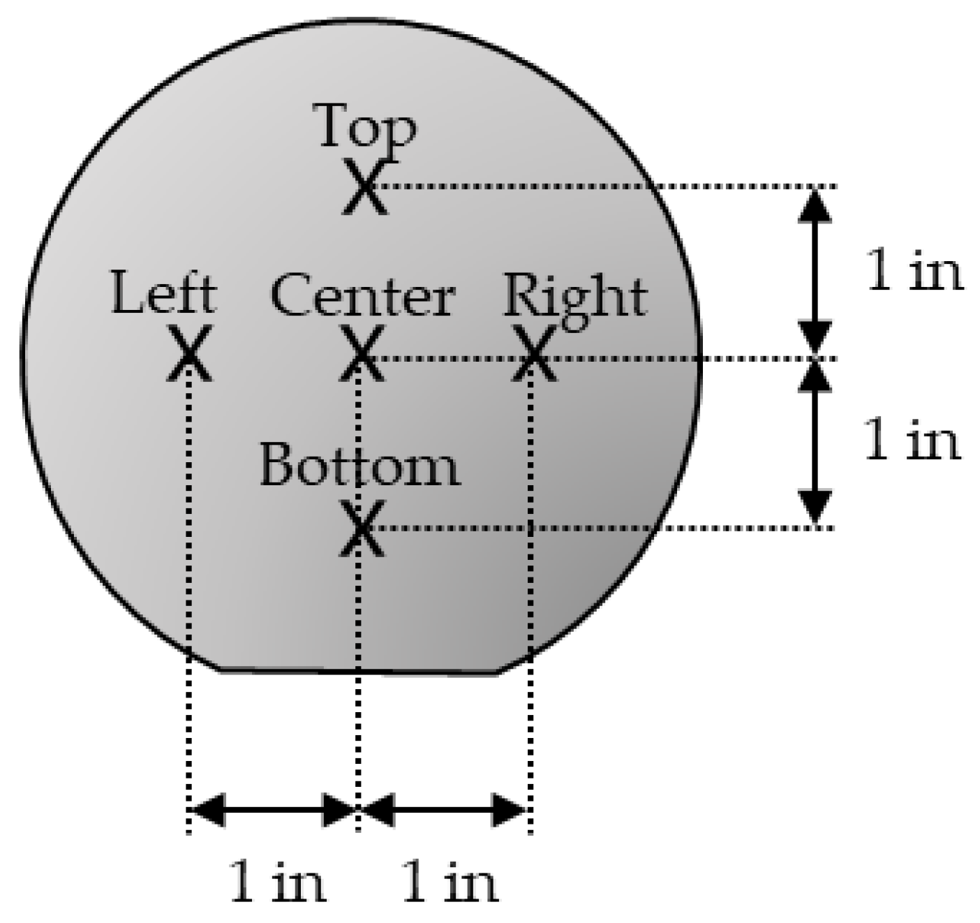
| Location | Thickness (nm) | |
|---|---|---|
| 100 nm SiC | 300 nm SiC | |
| Center | 98.4 | 307.8 |
| Left | 97.7 | 292.6 |
| Right | 99.0 | 306.5 |
| Top | 98.1 | 302.7 |
| Bottom | 99.2 | 300.0 |
| Average | 98.5 | 301.9 |
Publisher’s Note: MDPI stays neutral with regard to jurisdictional claims in published maps and institutional affiliations. |
© 2022 by the author. Licensee MDPI, Basel, Switzerland. This article is an open access article distributed under the terms and conditions of the Creative Commons Attribution (CC BY) license (https://creativecommons.org/licenses/by/4.0/).
Share and Cite
Kim, Y.Y. Thermal and Mechanical Properties of Amorphous Silicon Carbide Thin Films Using the Femtosecond Pump-Probe Technique. Materials 2022, 15, 2165. https://doi.org/10.3390/ma15062165
Kim YY. Thermal and Mechanical Properties of Amorphous Silicon Carbide Thin Films Using the Femtosecond Pump-Probe Technique. Materials. 2022; 15(6):2165. https://doi.org/10.3390/ma15062165
Chicago/Turabian StyleKim, Yun Young. 2022. "Thermal and Mechanical Properties of Amorphous Silicon Carbide Thin Films Using the Femtosecond Pump-Probe Technique" Materials 15, no. 6: 2165. https://doi.org/10.3390/ma15062165
APA StyleKim, Y. Y. (2022). Thermal and Mechanical Properties of Amorphous Silicon Carbide Thin Films Using the Femtosecond Pump-Probe Technique. Materials, 15(6), 2165. https://doi.org/10.3390/ma15062165