Article

Structure and Electrical Behavior of Hafnium-Praseodymium Oxide Thin Films Grown by Atomic Layer Deposition

1
Institute of Physics, University of Tartu, W. Ostwaldi 1, 50411 Tartu, Estonia
2
Department of Electronics, University of Valladolid, Paseo Belén 15, 47011 Valladolid, Spain
*
Author to whom correspondence should be addressed.
Materials 2022, 15(3), 877; https://doi.org/10.3390/ma15030877
Submission received: 19 December 2021 / Revised: 13 January 2022 / Accepted: 19 January 2022 / Published: 24 January 2022
(This article belongs to the Special Issue Atomic Layer Deposition: From Fundamentals to Applications)

Abstract

:
Crystal structure and electrical properties of hafnium-praseodymium oxide thin films grown by atomic layer deposition on ruthenium substrate electrodes were characterized and compared with those of undoped HfO2 films. The HfO2 reference films crystallized in the stable monoclinic phase of HfO2. Mixing HfO2 and PrOx resulted in the growth of nanocrystalline metastable tetragonal HfO2. The highest relative permittivities reaching 37–40 were measured for the films with tetragonal structures that were grown using HfO2:PrOx cycle ratio of 5:1 and possessed Pr/(Pr + Hf) atomic ratios of 0.09–0.10. All the HfO2:PrOx films exhibited resistive switching behavior. Lower commutation voltages and current values, promising in terms of reduced power consumption, were achieved for the films grown with HfO2:PrOx cycle ratios of 3:1 and 2:1 and showing Pr/(Pr + Hf) atomic ratios of 0.16–0.23. Differently from the undoped HfO2 films, the Pr-doped films showed low variability of resistance state currents and stable endurance behavior, extending over 104 switching cycles.

1. Introduction

HfO2, as a high-permittivity metal oxide, has attracted marked attention as a functional component of different nanoelectronic devices. HfO2 films have been studied and exploited as gate dielectric layers in both planar [1] and three-dimensional (3D) Fin-type [2] field-effect transistors. In order to modify the phase composition and enhance the functionality of the films, HfO2 has been doped with foreign metals or metal oxides. For example, Al-doped phase-stabilized HfO2 has been investigated as a dielectric for volatile dynamic random access memories [3]. In addition, stabilization of orthorhombic phase of HfO2 by doping with aluminum [4,5] or praseodymium [6] has been reported to cause the appearance of ferroelectric behavior, opening up routes to HfO2-based nonvolatile memories.
Regarding other potential applications of HfO2, resistive switching (RS) memory devices [7,8,9,10,11,12,13,14,15,16,17] are of significant importance. RS media based on metal oxides have been of interest for materials scientists and engineers over several decades, dating back to the beginning of 1960-ies [7]. The diversity in the choice of the materials suited to this application is still large, as one can decide on the basis of several recent reviews [7,8,9,10]. Amongst the metal oxide thin films under investigation, different compounds, such as TiO2, Al2O3, Ta2O5, ZrO2, or HfO2, can be considered.
HfO2 thin films have been examined as RS media in several studies [12,13,14,15,16,17]. At the same time, to improve the RS performance, the effect of doping has also been investigated. For instance, aluminum has been used as a dopant in RS HfO2 films [18,19]. In a long list of other dopants used in oxide films, praseodymium (Pr) is the one that has been applied to improve RS properties of CeO2 [20] and ZnO [21]. Moreover, Pr has found application as a component of a rather complex compound, Pr0.7Ca0.3MnO3, examined as RS media in a number of studies [22,23,24,25,26,27]. In the case of HfO2, Pr has mainly attracted attention as a dopant allowing stabilization of metastable phases with ferroelectric properties and high permittivity values [6]. These results led us to a conclusion that the further investigation of Pr-doped HfO2 as an electronic material could be of significant interest, especially because the Pr impurities might also influence the RS performance of HfO2.
Among the methods that can be used for the deposition of HfO2 thin films, atomic layer deposition (ALD) is the one that allows conformal coating of substrates with complex shapes [3]. For this reason, the method is of particular importance in the production of electronic devices with 3D integration [2,3]. The HfO2 thin films have been grown by ALD from different hafnium precursors [4,5,13,14,15,18,19,28] of which HfCl4 is a carbon-free metal precursor allowing self-limited ALD-type growth in an extremely wide temperature range extending from 225 to 940 °C [28]. H2O has been the most common oxygen precursor applied in ALD of HfO2. However, ozone (O3) as a hydrogen-free oxygen precursor has also been exploited for ALD together with HfCl4 [29,30,31,32]. As HfCl4 and O3 had advantages in the deposition of films with low contamination levels, the ALD process based on these precursors was also employed in the present work.
Praseodymium oxide (PrOx) thin films have been grown using chemical vapor deposition [33] as well as ALD [34] routes based on Pr(thd)3 (thd = 2,2,6,6-tetramethyl-3,5-heptanedione). The paper by Hansen et al. [34] implies that H2O does not serve as an appropriate co-reactant together with Pr(thd)3 because this precursor combination does not yield films with well-developed crystallinity and sufficient thickness uniformity. Another study on crystallization in lanthanide oxides [35] has indicated that PrOx films can be grown at 300 °C from Pr(thd)3 and O3. However, the films tend to be of multiphase composition, containing Pr6O11 and cubic PrO2 phases due to the ability of this lanthanide to form Pr3+ and Pr4+ oxides and the latter’s mixed phases.
Mixed PrOx and hafnium oxide films have been grown by ALD using Pr(thd)3, HfCl4, and O3 as the precursors [36]. In these experiments, the effects of deposition process parameters on the growth rate, crystal structure, phase composition, and optical properties (refractive index, optical bandgap, and photoluminescence efficiency) of the films were characterized [36]. The results revealed that the main phases observed in the praseodymium oxide films were PrO2 formed at 225–250 °C, Pr6O11 formed at 275 °C, and Pr7O12 and Pr6O11 formed at 300–325 °C. The studies on ALD of HfO2 from HfCl4 and O3 [32] have revealed that the monoclinic phase is predominantly obtained in the thicker (>40 nm) films at the substrate temperatures ranging from 225 to 600 °C. However, in the thinner films, the metastable cubic, tetragonal, or orthorhombic phase has also been observed [32]. Pr-doping stimulated the growth of the metastable phases while at sufficiently high Pr concentrations; only the tetragonal t′-form has been obtained in the films [36].
In nanoelectronics, ruthenium (Ru), as a noble metal with a high work function, has been of interest and studied as an electrode material of dynamic random access memory capacitors [37,38,39,40] with high permittivity dielectrics and very high capacitance density values [37]. Ru has also been applied as an electrode material of RS stacks [41,42,43]. Ru electrodes of RRAM devices have been directly contacted to Nb2O5 [44], tantalum oxide [43,45], or HfO2 films [41]. Depending on the processes investigated, the Ru electrodes [43] and/or switching metal oxide layers [42,46] may have been grown by ALD.
Although RS can be based on several underlying mechanisms, the switching phenomena in the metal–insulator–metal stacks with metal oxide dielectrics and electrochemically inactive metal electrodes are usually governed by the valence change mechanism (VCM) [46,47]. In this type of RS media, conductive filaments are formed by oxygen vacancies and grow in the dielectric until they connect metal electrodes. To create these filaments for the first time, it is usually necessary to perform an electroforming process applying voltage values that are higher than those needed later for RS [48,49]. Thereafter, using voltage with inverted polarity, the filament can be partially disrupted (RESET event). To form the conductive filament again (SET event), a voltage with the same polarity as in the electroforming process, but with a much lower value, can be applied [50]. VCM has been suggested to be the main RS mechanism in the structures with HfO2 dielectric and with inert metal electrodes [51,52]. Recently, the conductive filamentary model has been described in an RS medium consisting of alloyed HfTiOx films in silicon-based contact hole structures where the oxide was grown by ALD from tetrakisethylmethyl(amino) hafnium, titanium tetraisopropoxide, and water [53]. The VCM of RS has also been observed in the case of other oxides. For instance, there is experimental evidence of this filamentary conduction in Ta2O5-based films [54]. Therefore, the same RS mechanism was expected to appear in Pr-doped HfO2 as well.
The present work was performed to investigate the effect of Pr-doping on the electrical properties of HfO2, in particular, on the permittivity and RS performance. High permittivity together with high bandgap values is important in applications where HfO2 is used as a high-permittivity gate or capacitor dielectric. Earlier studies have revealed that Pr doping of HfO2 causes an increase in the bandgap values and stabilization of a metastable tetragonal phase [36] that was expected to lead to the permittivity increase. A goal of this work was to obtain experimental data on the permittivity of Pr-stabilized metastable HfO2. Another goal of this work was to investigate if the stabilization of the metastable phase and increase in the bandgap energy influence the RS performance, particularly the low to high resistance state ratio during RS and the stability of that ratio in terms of the endurance of such samples on ruthenium electrodes.

2. Materials and Methods

The Pr-doped HfO2 films studied in this work were deposited in an in-house built hot-wall flow-type ALD reactor [55] at 325 °C using HfCl4 (99.9 %, Aldrich Chemicals Co. St. Louis, MO, USA) and O3 as the precursors for deposition of HfO2 [32], and Pr(thd)3 (Volatec Oy, Porvoo, Finland) and O3 for adding PrOx to the film material [36]. Nitrogen (99.999%, AS Linde Gas, Tallinn, Estonia) was the carrier as well as purging gas in these experiments. The deposition process parameters were similar to those used earlier [36]. During the deposition, the net gas pressure in the reactor was kept at 200–220 Pa. O3 was produced from O2 (99.999% purity, AS Linde Gas, Tallinn, Estonia) using a BMT 802N ozone generator (BMT Messtechnik, Stahnsdorf, Germany). The O3 concentration, measured by a BMT 964 ozone analyzer (BMT Messtechnik, Stahnsdorf, Germany) in the O3/O2 mixture at the outlet of the O3 generator, was 240–260 g/m3. The partial pressure of the O3/O2 mixture was set at 22 Pa in the reaction chamber during the oxygen precursor pulses.
The Ru bottom electrodes were deposited on Si(100) substrates at room temperature by DC-magnetron sputtering in Ar (99.999%) environment using a Ru (99.95%) planar target of 25 mm in diameter. The pressure during the sputtering process was 3 × 10⁻³ mbar, the DC-power was 2 W and the distance between target and substrate was 60 mm.
For the deposition of Pr-doped HfO2, supercycles—including one cycle of Pr(thd)3-O3 per 2–5 cycles of HfCl4-O3—were repeated 25–50 times to obtain 19–50-nanometer thick Pr-doped films studied in this work. Each ALD cycle used for deposition of HfO2 included a HfCl4 pulse, purge, O3 pulse, and another purge with durations of 5, 2, 5, and 5 s, respectively, while those used for deposition of PrOx included a Pr(thd)3 pulse, purge, O3 pulse, and purge with durations of 5, 2, 5, and 5 s, respectively. No post-deposition annealing was applied for samples studied in this work.
The crystalline phases formed in the films were determined by the grazing incidence XRD (GIXRD) method using an X-ray diffractometer SmartLab (Rigaku, Tokyo, Japan) and Cu Kα radiation. The incidence angle chosen for the GIXRD measurements was 0.42°, corresponding to the scattering depth of 20 nm in cubic PrO2 and 11 nm in monoclinic HfO2 [36]. The diffractometer was also employed for X-ray reflection (XRR) measurements to determine the film thickness and surface roughness values. Additionally, the film thicknesses were measured with a GES5E spectroscopic ellipsometer (Semilab Sopra, Budapest, Hungary). Combining these two methods, the thicknesses of thinner (19–28 nm) films were determined with an accuracy better than ±2 nm while those of thicker (50–65 nm) films were obtained with an accuracy of ±3 nm. The mass thicknesses and elemental compositions of the films were determined with X-ray fluorescence (XRF) analyzer ZSX400 (Rigaku, Tokyo, Japan). Scanning electron microscope (SEM) Helios NanoLab 600 (FEI Company, Hillsboro, OR, USA) was used in a high-resolution mode (at an acceleration voltage of 10 kV and electron beam current of 86 pA) to characterize the surface microstructure.
For the electrical measurements, titanium top electrodes with circular geometry and thicknesses of 50 nm were electron-beam evaporated on the dielectric through a shadow mask at 230 °C. The Ti electrodes used in the measurements had areas of 0.002 and 0.052 mm2. Electrical measurements were carried out in a probe station using a Keithley 4200-SCS semiconductor analyzer (Keysight Technologies, Cleveland, OH, USA). In the DC measurements, the bias voltage was applied to the top electrode while the bottom electrode remained grounded. To initiate RS, every sample required an electroforming procedure that was carried out as a voltage sweep with positive bias using a current compliance set at 1 μA to avoid irreversible breakdown of devices. In general, the electroforming took place between 7 and 13 V. The current–voltage (I-V) curves were obtained by applying positive and negative voltage sweeps to switch between the resistance states (bipolar RS), while the memory maps [56,57] were measured by reading the current value at 0.1 V after applying every increasing (or decreasing) voltage value used in the I-V envelope curves. To carry out the endurance measurements, a high number of relatively fast RS cycles were recorded. Each cycle was defined by a voltage pulse sequence of Vset, 0.1 V, –Vreset, and 0.1 V with switching pulse time durations of 0.1 s for Vset as well as for Vreset. Capacitance frequency measurements were carried out by applying a 30-millivolt signal without a DC bias in the 10 kHz–1 MHz frequency range.

3. Results and Discussion

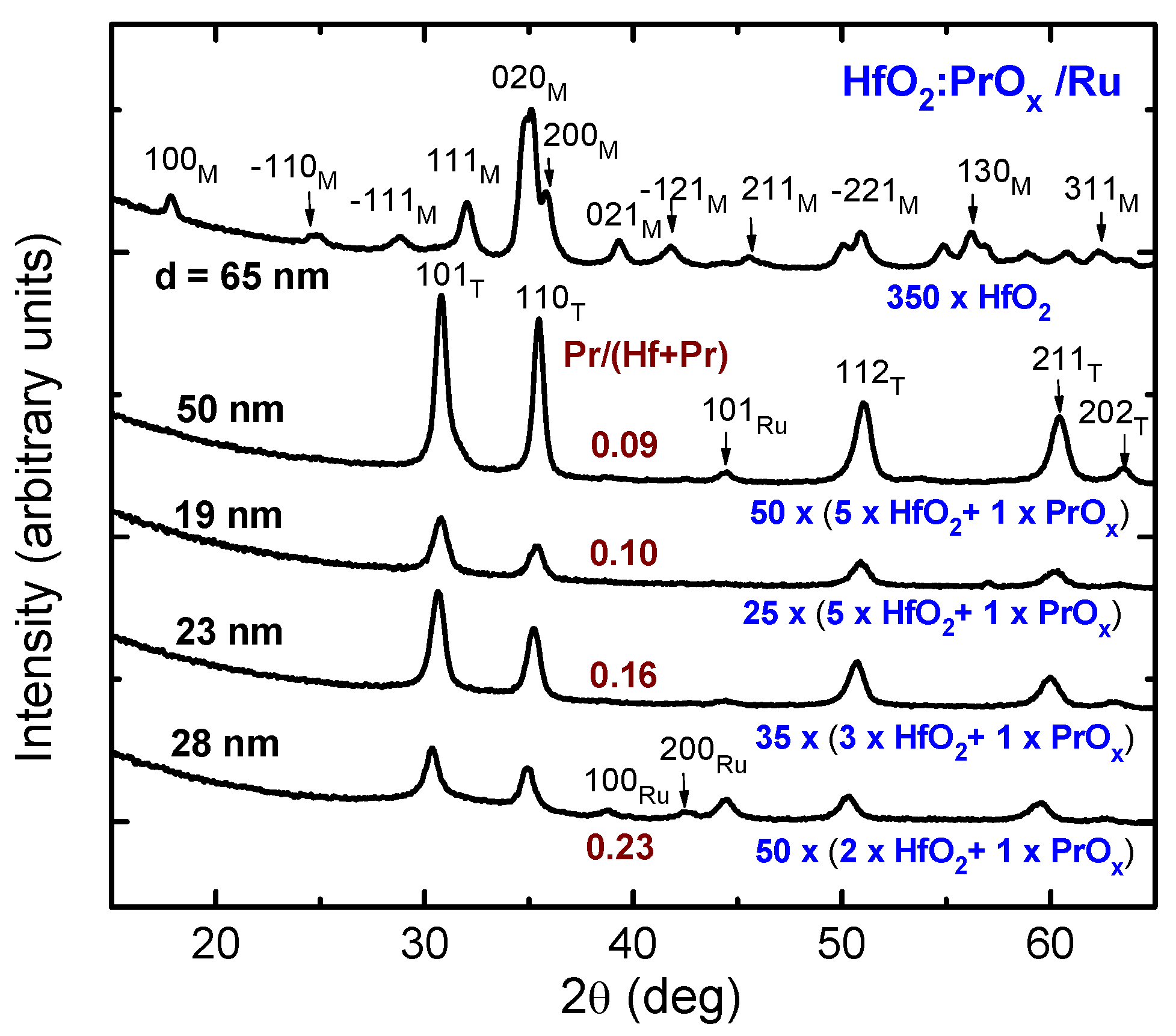
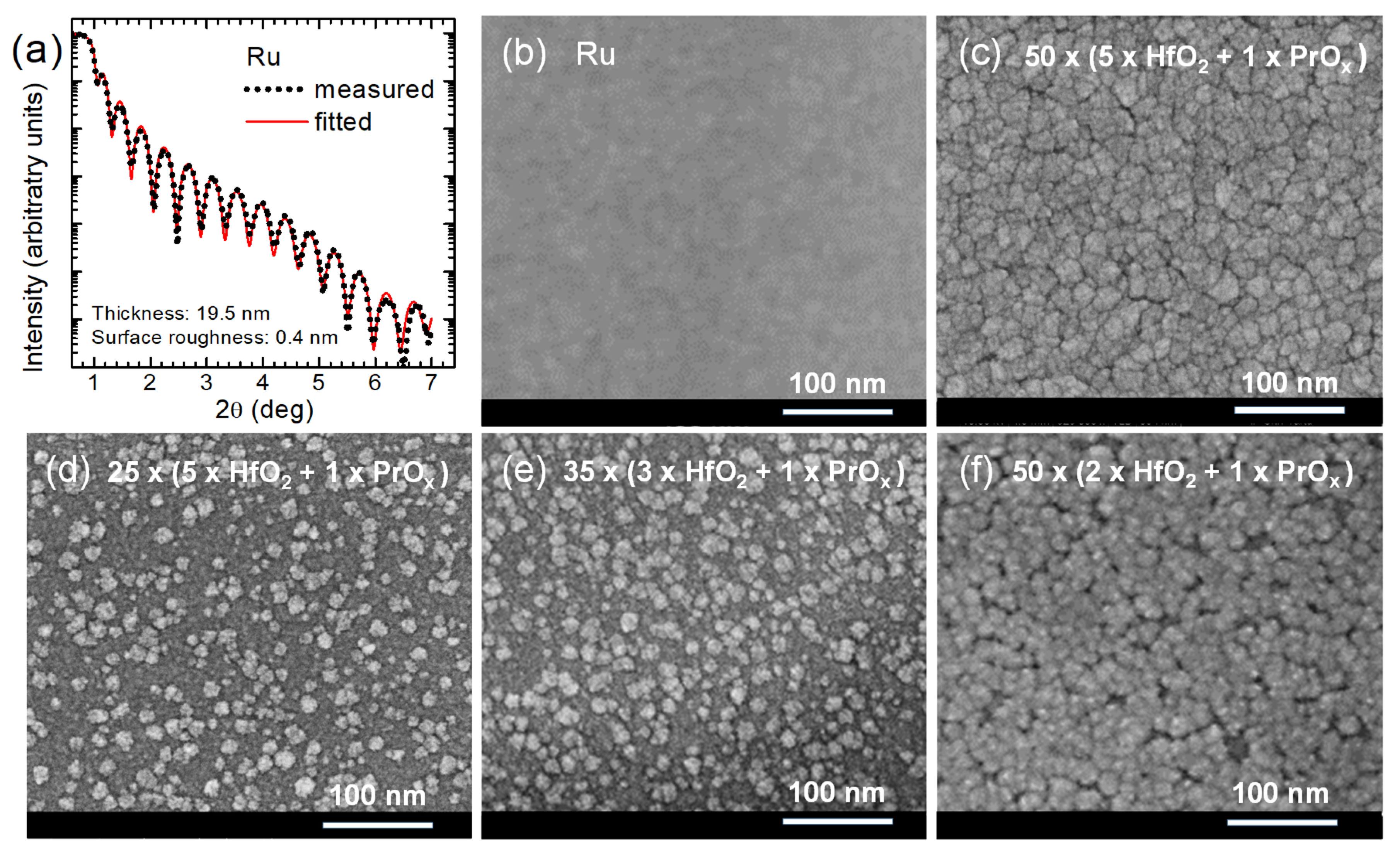
3.1. Composition and Structure

The Pr/(Hf + Pr) atomic ratio in the HfO2:PrOx films was appreciably correlated with the ratio of HfO2 and Pr2O3 deposition cycles (Figure 1) and equaled to 0.23, 0.16, and 0.10 in the 28-, 23-, and 19-nanometer thick films, grown using the HfO2:PrOx cycle ratios of 2:1, 3:1, and 5:1, respectively. In the 50-nanometer thick film grown using the HfO2:PrOx cycle ratio of 5:1, the Pr/(Hf + Pr) atomic ratio was 0.09.
As expected, the Pr content influenced the crystal structure of the HfO2:PrOx films. As can be seen in Figure 2, the 65-nanometer thick HfO2 reference film, i.e., the one which did not contain PrOx, was unambiguously crystallized in the form of the stable monoclinic polymorph. Furthermore, the expected and also obvious effect of the doping was the stabilization of a metastable polymorph. It should be mentioned, however, that the distinction between metastable cubic, tetragonal, and even orthorhombic phases of HfO2 was quite complicated, considering the small crystallite sizes accompanied by peak broadening and possible effects of doping and substrate structure, causing shifts in the peak positions. The corresponding reflections, peaking at 30.3, 35.5, 50.3, 60.5, and 63.0 degrees (Figure 2), were attributable to the 101, 110, 112, 211, and 202 reflections of tetragonal HfO2 (PDF card 01-078-5756). At the same time, the reflections might also be assigned as 111, 002, 022, 113, and 222 reflections of the cubic HfO2 (PDF card 96-900-9017), or as 111, 020, 022, 113, and 311 reflections of the orthorhombic HfO2 (PDF card 00-021-0904). However, it is worth mentioning that the refinement of similar diffraction patterns of Pr-doped HfO2 thin films grown by ALD on silicon substrates to thicknesses of 140–328 nm revealed the formation of tetragonal t′ form rather than other phases of HfO2 in the films with Pr/(Pr + Hf) atomic ratios ≥ 0.095 [36]. The tetragonal t′ form [58] is characterized by the relatively small tetragonality of its lattice (with lattice parameter ratios c/a ranging from 1.004 to 1.012 for the pseudo-fluorite unit cell), and therefore is an intermediate structure form between the cubic and tetragonal HfO2. Nevertheless, it is also possible that the structure of the relatively thin films deposited on Ru in the present work had not been fully formed and, for this reason, was of a multiphase nature. In particular, low GIXRD reflection intensities of the thinner films grown with a HfO2:PrOx cycle ratio of 5:1 indicated the presence of amorphous and/or nanocrystalline phases with poorly developed structure in the films.
Although no direct correlation between the resistance state values and dielectric thickness had been observed in the VCM type RS media, based on HfO2 [59] and other media [60], the dependence of the permittivity and RS performance on the structure development related to the dielectric thickness (Figure 2) could not be neglected. However, the results of electrical measurements presented below were dominantly influenced by the chemical and phase composition rather than by the thickness of the dielectric. For this reason, the further downscaling of the thickness was not studied in the present work.
The fitting of XRR data, measured for a 19.5-nanometer-thick Ru film used as a bottom electrode (Figure 3a), yielded a surface roughness value as low as 0.4 ± 0.2 nm. Thereby, the density of Ru was found to be 12.5 g/cm3, that is, close to the bulk value. The SEM studies confirmed the almost featureless and artifact-free nature of Ru electrode films (Figure 3b), allowing one to rely on smooth contact interfaces between the electrode and the RS medium. This was an important result because the SET events of the RS processes took place at positive voltages applied to the top electrodes. In such a case, the smoothness of the bottom electrode was assumed to reduce the parasitic leakage currents related to the electronic conduction and allowed us to expect reliable and reproducible electrical performance, uniform and stable over the electrode matrix formed on a sample used for electrical studies.
The thicker dielectric film grown using HfO2:PrOx cycle ratio of 5:1 evidently consisted of densely packed grains (Figure 3c). A surface roughness of 1.9 nm, obtained from XRR measurements of this film, was notably higher than that of the Ru surface. For comparison, the surface roughness of a HfO2 film of similar thickness was 1.7 nm. Smaller but distinctive grain-like features were observed by SEM on the surfaces of 2–3 times thinner oxide films (Figure 3d–f). The surface roughness values of these films grown using the HfO2:PrOx cycle ratios of 5:1, 3:1, and 2:1 were 0.6, 1.4, and 1.2 nm, respectively. It is worth noting that the SEM images as well as surface roughness values were consistent with the degrees of crystallization characterized by GIXRD (Figure 2).

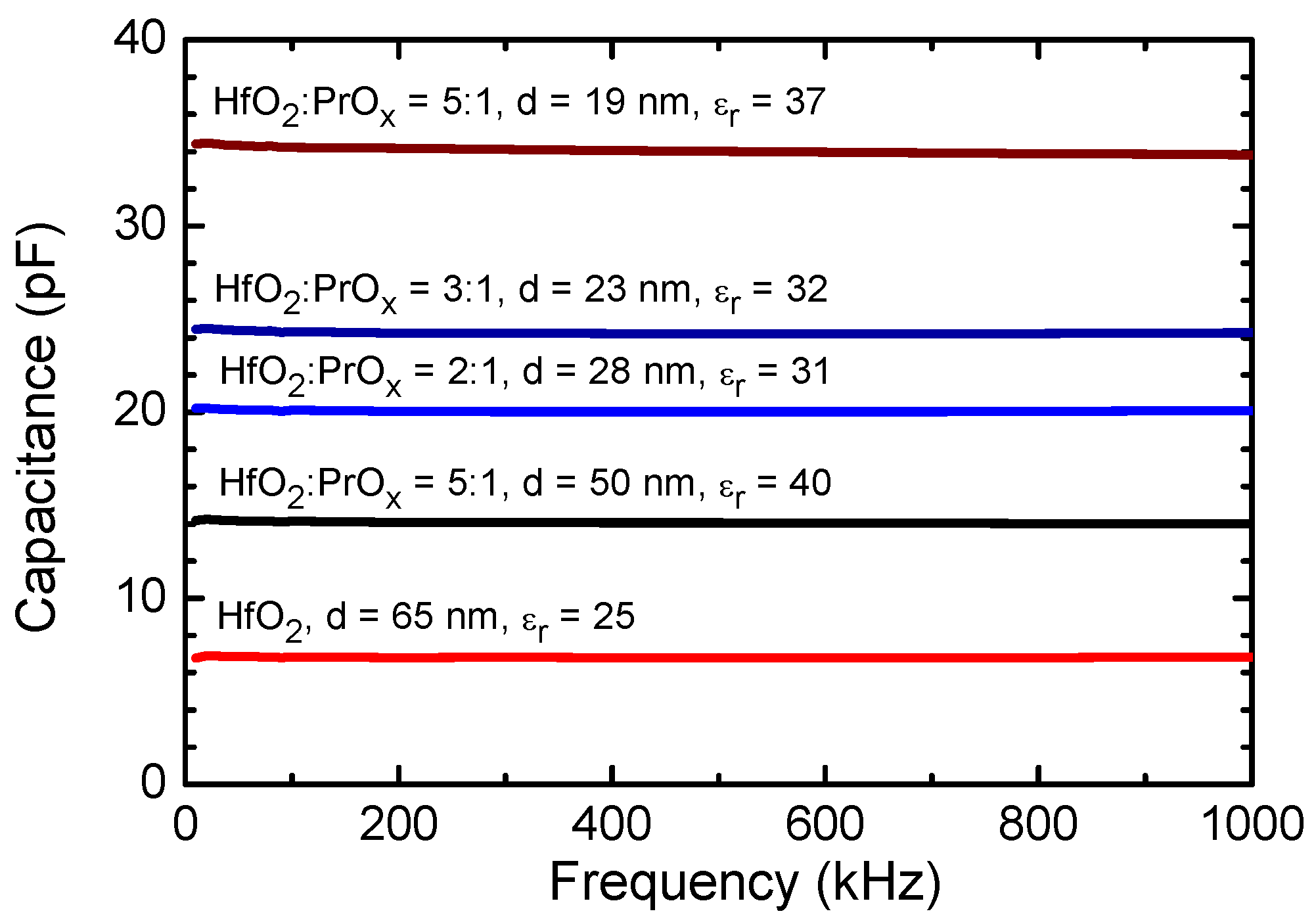
3.2. Dielectric Properties

Figure 4 depicts the results of capacitance frequency measurements carried out on HfO2:PrOx films deposited on common Ru bottom electrodes and supplied with top electrodes arranged in a matrix. The capacitance did not show marked dispersion in a frequency range of 10–1000 kHz (Figure 4). This result could be considered as a plausible indication of the insignificant role of the relatively free space charge. Expectedly and most clearly, the capacitance correlated to the film thickness. However, the relative permittivity that depended on the phase composition of the HfO2:PrOx films (Figure 2) also influenced the capacitance values.
The relative permittivity values were calculated from the mean capacitance values measured at 100 kHz. The highest permittivities, 37 and 40, were achieved from the calculations for the films deposited using a HfO2:PrOx cycle ratio of 5:1 to the thicknesses of 19 and 50 nm, respectively. The GIXRD data (Figure 2) and results of the more complex analysis performed earlier [36] indicated that both films contained tetragonal phase (t′ form), with the most intense reflections of 101 and 110, apparent in their diffraction patterns. The 23 and 28 nm thick films that were grown using HfO2:PrOx cycle ratios of 3:1 and 2:1, and crystallized in the same metastable polymorph, possessed relative permittivities of 32 and 31, respectively. The lowest permittivity value that was equal to 25 was measured for the undoped HfO2 film, which was grown to the thickness of 65 nm, and contained monoclinic HfO2 (Figure 2).
Regarding the literature data, Zhao and Vanderbilt [61] obtained in their first-principles calculations that orientationally averaged static dielectric constants should be 29, 70, and 16 for the cubic, tetragonal, and monoclinic HfO2 phases, respectively. In this connection, the permittivity values measured in the present study might have been related to the polymorphic composition of the films under discussion (Figure 2). The permittivity values extending to 40 (Figure 4) could thus be due to the presence of the tetragonal HfO2 phase in the films. In this case, the value of the relative permittivity, although lower than that predicted by the first-principles calculations, could herewith be reasoned by the reduced tetragonality of the t′ form or possible co-existence of tetragonal, cubic, and amorphous phases in the corresponding films. In contrast, the relative permittivity value as high as 25 (Figure 4), measured for the undoped HfO2 film was higher than that attributed to the monoclinic HfO2 [61]. This might, supposedly, become explained by a minor contribution of metastable phases that could also be present in the films.
In earlier studies of Pr-doped HfO2 thin films that were grown by chemical solution deposition method and annealed at 800 °C, relative permittivity values of 23.5, 29.7, and 32.1 were obtained at Pr concentrations of 5, 10, and 15 mol%, respectively, while the corresponding value for an undoped HfO2 film was determined to be 18.3 [6]. The crystalline phases observed were the monoclinic one in the undoped films, the orthorhombic phase in the films with 5 mol% Pr, and the cubic phase in the films with 10 and 15 mol% Pr [6]. Comparing these results with those of theoretical calculations [61] and with the permittivity values obtained for ALD films in our work (Figure 4), one can conclude that the formation of the tetragonal structure was the main reason for the high permittivity values of our films deposited using a HfO2:PrOx cycle ratio of 5:1.
The decrease in the permittivity observed with the decrease of the HfO2:PrOx cycle ratio to 2:1 and increase of the Pr/(Pr + Hf) atomic ratio from 0.10 to 0.23 was probably caused by a decreasing amount of tetragonal phase in the films and/or decrease in the tetragonality of the t′ form of HfO2 with increasing concentration of Pr. The decrease in the tetragonality of the t′ form with increasing concentrations of rare-earth dopant in HfO2, has been observed, for instance, in the case of yttria-doped HfO2 [60]. Unfortunately, because of relatively wide reflections in the GIXRD patterns of our films (Figure 2), revealing this kind of change in the crystal structure was not possible in the present work.
Another effect that might have contributed to the permittivity decrease observed with the increase of the Pr/(Pr + Hf) atomic ratio from 0.10 to 0.23 was the doping anisotropy that was most significant in the films grown with a HfO2:PrOx cycle ratio of 5:1. In the growth direction of these films, the Pr concentration varied with a period of 0.8–1.0 nm, approximately. This value was evidently larger than the in-plane distance between Pr3+ or Pr4+ ions, provided that the solid-phase diffusion did not lead to uniform distribution of Pr in the films. For comparison, the Pr concentration was expected to vary with a period of 0.5–0.6 nm in the growth direction of the films deposited using a HfO2:PrOx cycle ratio of 2:1. In this case, the period of dopant concentration variation was closer to the in-plane distances between Pr3+ or Pr4+ ions and, for this reason, the Pr distribution was more uniform than that in the films deposited with a HfO2:PrOx cycle ratio of 5:1.
Finally, the lower permittivity of PrOx compared to that of tetragonal HfO2 could be a reason for the permittivity decrease observed for Pr-doped HfO2 with the decrease of the HfO2:PrOx cycle ratio from 5:1 to 2:1. According to the literature data, the relative permittivity values of polycrystalline PrOx films have ranged from 8 to 26 [62,63] being higher for Pr2O3 and lower for PrO2-rich films [62]. Therefore, to obtain the highest permittivity values, the Pr concentration in the Pr-doped HfO2 films should not exceed significantly the value corresponding to the transition from the monoclinic to the tetragonal phase.
The conductivity of metal oxide dielectrics is directly related to their bandgap widths. On the other hand, doping with foreign elements—otherwise beneficial in terms of the stabilization of high-permittivity phases—might introduce parasitic states in the bandgap which could, presumably, increase the conduction currents. For instance, in the case of doping HfO2 with praseodymium (oxide), Pr3+ ions have energy levels in the bandgap of HfO2 [64]. At the same time, however, the optical bandgap increased from 5.55–5.65 eV, determined for undoped HfO2, to 5.72–5.78 eV in the doped films, where Pr/(Pr + Hf) = 0.15–0.20 and a tetragonal phase was formed [36]. Notably, also the theoretical calculations have predicted a wider bandgap for the metastable tetragonal/cubic HfO2, compared to that of stable monoclinic HfO2 [65]. Therefore the bandgap widening compensates, at least to some extent, for the contribution of the additional states generated in the bandgap by doping, thereby enabling the formation of HfO2:PrOx films appreciably insulating in the capacitor structures and in the low resistance state of RS devices.

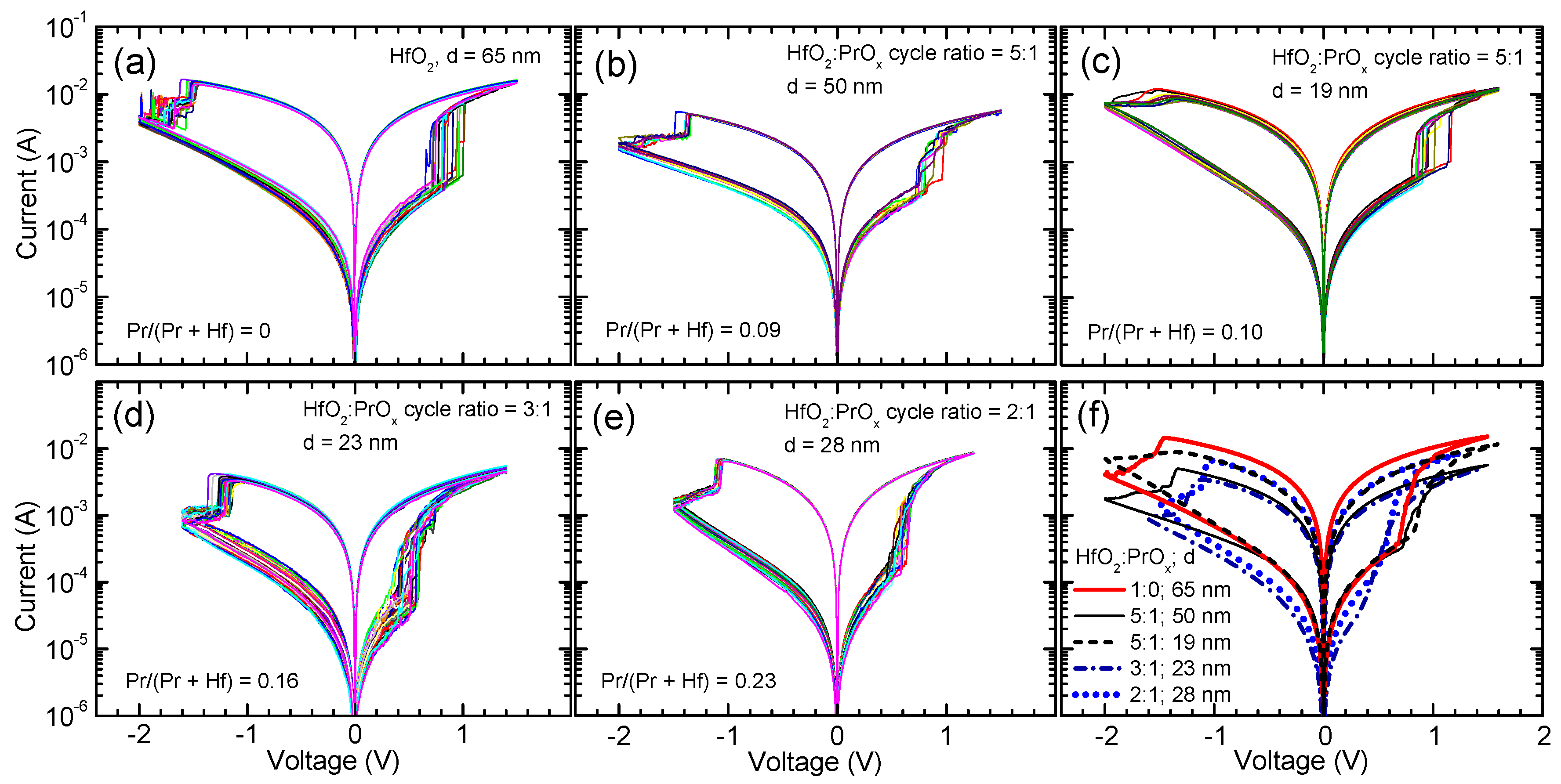
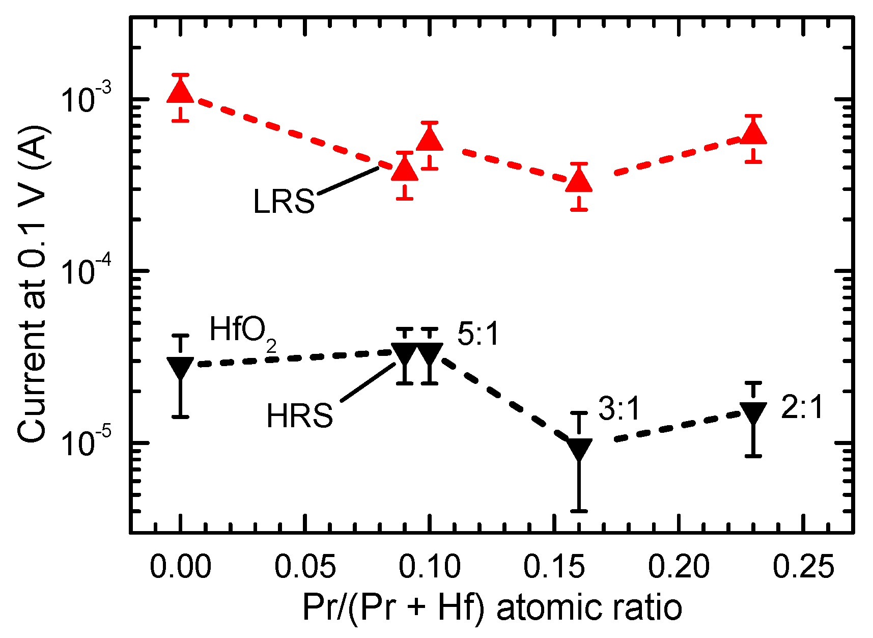
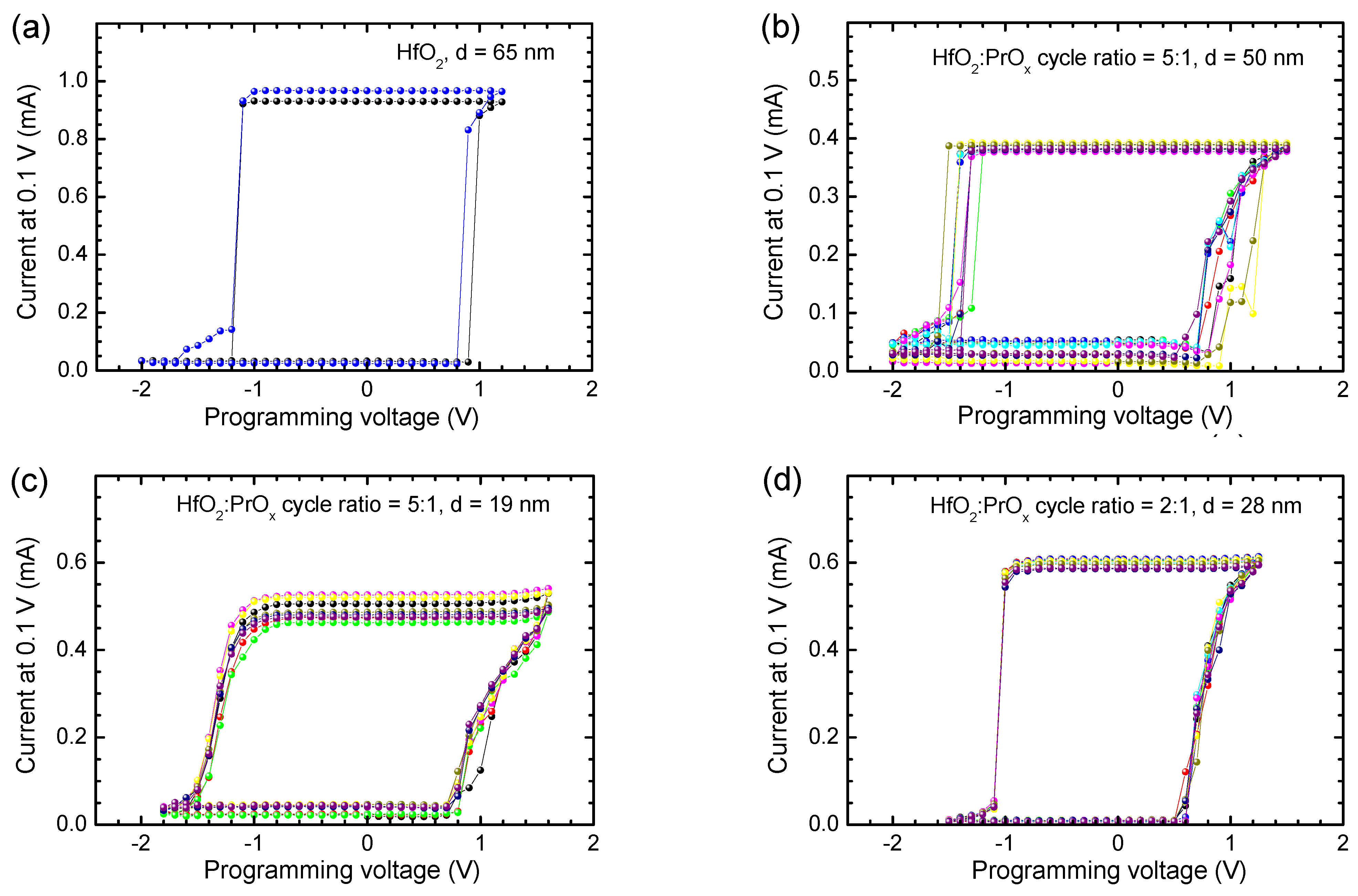
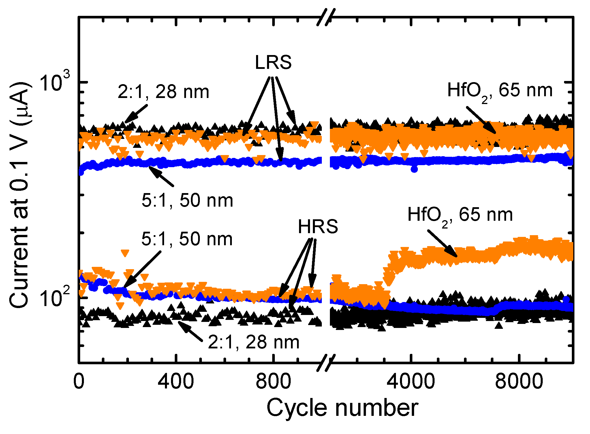
3.3. Resistive Switching

The HfO2 and HfO2:PrOx films, which were deposited in this work on Ru electrodes and supplied with Ti top electrodes, demonstrated RS behavior, expressed by clear current–voltage envelope curves characteristic of RRAM devices (Figure 5). The electroforming voltages did not vary systematically with the HfO2:PrOx ratio. All the samples demonstrated, however, an abrupt forming transitions at 11–13 V to a current value of 1 μA set as a compliance limit in order to prevent irreversible breakdown.
The nature of the switching process (Figure 5) was bipolar, meaning that in the SET process, the conductive filaments were formed applying positive voltage in relation to the Ru electrode, while in the RESET process, the conductive paths were disrupted by applying voltage of the opposite polarity. The smallest electrodes with the average area of 0.002 mm2 provided the most reliable results, that is, the initial electroforming process did not typically cause the dielectric breakdown, which otherwise would indicate issues with lateral homogeneity in the switching media.
The results depicted in Figure 5 and Figure 6 demonstrate that the Pr concentration in the RS layer influenced the commutation voltages, current values in the low-resistive state (ILR) and high-resistive state (IHR) as well as the ILR/IHR ratio. The increase in the Pr/(Pr + Hf) atomic ratio from 0 to 0.10 caused a decrease in ILR (Figure 5a–c and Figure 6) and a minor increase in the set voltages (Figure 5a–c). At the same time, no considerable changes in IHR appeared (Figure 6). As a result, the ILR/IHR ratios of the films that were grown using a HfO2:PrOx cycle ratio of 5:1 were lower than that of un-doped HfO2.
Comparison of the data for films with similar Pr/(Pr + Hf) atomic ratios (0.09 and 0.10) and very different thicknesses (50 and 19 nm, respectively) revealed minor differences in ILR (Figure 5b,c and Figure 6). However, as can be seen in Figure 6, these differences were comparable to the experimental uncertainty related mainly to the deviation of results in successive measurements of the current-voltage (I-V) curves.
With the increase of the Pr/(Pr + Hf) atomic ratio to 0.16, obtained at a HfO2:PrOx cycle ratio of 3:1, the set and reset voltages and IHR decreased while ILR/IHR increased to a level exceeding that of undoped HfO2 (Figure 5d and Figure 6). The further increase of the Pr/(Pr + Hf) atomic ratio to 0.23, observed in the films grown with a HfO2:PrOx cycle ratio of 2:1, did not influence the commutation voltages and ILR/IHR significantly (Figure 5d–f). However, ILR and IHR somewhat increased when compared to the corresponding values of the film grown using a HfO2:PrOx cycle ratio of 3:1 (Figure 6).
Besides the envelope I-V curves describing current values measured at the variable bias voltage values (Figure 5), memory maps were recorded at a constant reading voltage as well (Figure 7). In the latter case, the conduction currents were read at a voltage of 0.1 V in between the sequential programming voltage pulses. Two clearly defined plateaus were reached between sequential SET and RESET events (Figure 7). I-V loops, which can be termed as memory maps, were thus formed with prominently expressed memory windows between the high and low current states during multiple voltage loops (Figure 7).
The memory maps supported the results depicted in Figure 5 and Figure 6, showing that narrower windows between the low and high resistivity states, that is lower ILR/IHR ratios, were obtained for the reference HfO2 films (ILR/IHR ≈ 30, Figure 7a) and especially for the films deposited using HfO2:PrOx cycle ratio of 5:1 (ILR/IHR ≈ 10, Figure 7b,c). The window between the low and high resistivity states was much wider in the case of samples containing oxide media grown with HfO2:PrOx cycle ratios of 3:1 (not shown) and 2:1 (ILR/IHR ≈ 60, Figure 7d). Hence, rather than being a monotonic function of the Pr-content, the ILR/IHR ratio possessed a minimum value at Pr/(Pr + Hf) atomic ratios of 0.09–0.10, that is, at the HfO2:PrOx cycle ratio of 5:1. Earlier a significant dependence of RS performance on the doping level has been reported for Pr-doped ZnO films where the best functional ratio between resistance states appeared in the case of a certain stoichiometry [66]. The argument of an optimal composition has also been supported by the first-principles calculations made on HfOx-based films [67]. Furthermore, thicknesses may also become more optimized at certain film stoichiometries [68], and would, consequently, require further more detailed parametrization.
Comparing the results depicted in Figure 5, Figure 6 and Figure 7 with the GIXRD patterns (Figure 2), one can see that the ILR decrease, caused by the increase of Pr/(Pr + Hf) to 0.09–0.10, was evidently related to the formation of the metastable phase in the films. The wider bandgap of this phase [36] and possible compensation of oxygen vacancies because of Pr-doping are the plausible reasons for this ILR decrease. A probable reason for why the IHR value did not decrease and, correspondingly, the ILR/IHR value decreased was the presence of some inclusions of monoclinic phase in the films deposited using a HfO2:PrOx cycle ratio of 5:1. An evidence of the monoclinic phase is a tail on the right side of the 30.3° reflection in the diffraction pattern of the 50-nm thick films grown with this cycle ratio (Figure 2). This tail was evidently related to the contribution of the 111 reflection of the monoclinic phase. Although the small amounts of the monoclinic phase were not able to have a marked effect on the low-resistive state, the contribution of those to the much lower IHR values was still an expected result. Correspondingly, the absence of the monoclinic phase in the films grown with HfO2:PrOx cycle ratios of 3:1 and 2:1 and the formation of a more homogeneous crystalline phase in these films were reasons for lower IHR and higher ILR/IHR values obtained. The latter films also possessed somewhat lower commutation voltages (Figure 5f and Figure 7) than the rest of the samples did. This observation implies that the media which contain higher amounts of praseodymium and only metastable nanocrystalline phases might become better suited to low-power applications. Higher mobility of oxygen ions in these films might be one possible reason for lower commutation voltages observed.
Endurance measurements were carried out for samples with different doping levels to determine their reliability and resistance state variability during fast writing, erasing, and reading operations. In these measurements, a current compliance of 5 mA was set in order to prevent the irreversibly breaking of dielectrics when applying the commutation voltages in a short period of time. The use of compliance has been shown to improve the endurance characteristics in HfOx-based RRAM [69]. However, the same functional windows between the high and low resistance states were not expected when comparing the results of endurance studies with the current-voltage envelope curves or memory maps.
First of all, the endurance characteristics presented in Figure 8 revealed higher stability of Pr-doped HfO2 media compared to that of undoped HfO2. In the case of samples with undoped HfO2, the first instabilities in ILR as well as IHR appeared after applying a few hundred cycles, while a marked increase in IHR was observed after 3000 cycles. In contrast, the RS layer grown using a HfO2:PrOx cycle ratio of 2:1 showed very stable ILR as well as IHR values up to the end of the endurance measurements (Figure 8). Therefore, the Pr-doping of HfO2 and/or formation of metastable (tetragonal) phase in the RS medium play a significant in producing memory cells with superior RS performance.
An even more interesting performance was observed in the case of samples with Pr-doped HfO2 deposited using a HfO2:PrOx cycle ratio of 5:1 that yielded films with Pr/(Pr + Hf) atomic ratios of 0.09–0.10. Figure 8 demonstrates that with an increasing number of switching cycles, the IHR value of a 50-nanometer thick film considerably decreased while the ILR value increased resulting in a marked increase in the ILR/IHR ratio. It is noteworthy that a similar performance was observed for a 19-nanometer thick films with a Pr/(Pr + Hf) atomic ratio of 0.10. In both cases, the changes in IHR, ILR, and ILR/IHR were relatively smooth without significant random fluctuations of the current values. Therefore, it seems that the conductive filaments were additionally electroformed (stabilized) in this kind of RS medium during the endurance studies. Phase transitions leading to the formation of a more uniform crystal structure and/or more uniform distribution of Pr3+/Pr4+ ions in the vicinity of switching filaments can be considered as the main mechanisms causing this kind of modification of the RS medium.
Comparison of our results with literature data confirmed the excellent performance of Pr-doped HfO2 studied in this work compared to that of many other HfO2-based undoped and doped RS media. Typical ILR/IHR values reported [16,70,71,72,73,74,75] have ranged from one to two orders of magnitude being well comparable to the corresponding values obtained in our work. However, ILR/IHR values as high as three orders of magnitude have also been reported for samples with optimized electrode structure [76]. In most cases, the endurance tests, if performed, have been limited to 1000 switching cycles [70,71,73,75] but reports about endurance tests up to 105 [72,74] and 108 [16] switching cycles have also been published. Comparing the results described in the latter papers with those obtained in our experiments one can still conclude that after optimization of the device processing procedures, Pr-doped HfO2 can also become a promising candidate for application in resistive switching random access memories.

4. Conclusions

Our studies of Pr-doped HfO2 thin films grown by ALD on ruthenium electrodes revealed superior properties of these films for different electronic applications. The films grown using HfO2:PrOx ALD cycle ratios, ranging from 5:1 to 2:1, crystallized in the tetragonal phase while the Pr/(Pr + Hf) atomic ratio ranged from 0.09 to 0.23 in these films. The relative permittivity values as high as 37–40 were measured for the films with Pr/(Pr + Hf) atomic ratios of 0.09–0.10. No considerable dependence of the permittivity on the measurement frequency was observed in a frequency range of 0.01–1 MHz. As the films with this composition have also high bandgap values (5.72–5.78 eV), as revealed in our earlier work, they could successfully be applied as capacitor and gate dielectrics.
Additionally, stable-resistive switching performance was obtained in metal–dielectric–metal structures with HfO2:PrOx dielectrics, ruthenium bottom electrodes, and titanium top electrodes. In the structures with as-grown dielectrics, the ILR/IHR ratios ranged from 10 in the case of dielectrics with Pr/(Pr + Hf) atomic ratios of 0.09–0.10 to 60 in the case of dielectrics with Pr/(Pr + Hf) atomic ratios of 0.16–0.23. The resistive switching layers with Pr/(Pr + Hf) atomic ratios of 0.16–0.23 showed also lower ILR, IHR, and commutation voltage values compared to corresponding parameters recorded for devices with undoped HfO2 dielectric. The endurance measurements demonstrated excellent stability of resistive switching in Pr-doped HfO2 during 104 switching cycles. Thus, Pr-doped HfO2 could be considered as a promising material for application in resistive switching memory devices as well.

Author Contributions

Conceptualization, K.K., L.A., S.D. and J.A.; methodology, G.V., L.A., J.A., H.G. and H.C.; investigation, G.V., L.A., A.K., P.R. and H.-M.P., resources, K.K., L.A. and H.C.; writing, K.K., G.V. and J.A.; funding acquisition, K.K., L.A., H.C. and S.D. All authors have read and agreed to the published version of the manuscript.

Funding

The work has partially been supported by Spanish Ministry of Science, Innovation and Universities grant TEC2017-84321-C4-2-R, with support of Feder funds; European Regional Development Fund project “Emerging orders in quantum and nanomaterials” (TK134); and Estonian Research Agency (projects PSG448 and PRG753).

Institutional Review Board Statement

Not applicable.

Informed Consent Statement

Not applicable.

Data Availability Statement

Not applicable.

Conflicts of Interest

The authors declare no conflict of interest.

References

  1. Huff, H.R.; Hou, A.; Lim, C.; Kim, Y.; Barnett, J.; Bersuker, G.; Brown, G.A.; Young, C.D.; Zeitzoff, P.M.; Gutt, J.; et al. High-k gate stacks for planar, scaled CMOS integrated circuits. Microelectron. Eng. 2003, 69, 152–167. [Google Scholar] [CrossRef]
  2. Tsormpatzoglou, A.; Tassis, D.H.; Dimitriadis, C.A.; Mouis, M.; Ghibaudo, G.; Collaert, N. Electrical characterization and design optimization of FinFETs with a TiN/HfO2 gate stack. Semicond. Sci. Technol. 2009, 24, 125001. [Google Scholar] [CrossRef]
  3. Kim, S.-G.; Hyun, C.-S.; Park, D.; Cho, T.-H.; Suk, J.-G.; Hong, H.-S.; Lee, K.-Y.; Oh, K.-S. Fully integrated 512 Mb DRAMs with HSG-merged-AHO cylinder capacitor. Solid-State Electron. 2006, 50, 1030–1034. [Google Scholar] [CrossRef]
  4. Mueller, M.; Mueller, J.; Singh, A.; Riedel, S.; Sundqvist, J.; Schroeder, U.; Mikolajick, T. Incipient ferroelectricity in Al-doped HfO2 thin films. Adv. Funct. Mater. 2012, 22, 2412–2417. [Google Scholar] [CrossRef]
  5. Florent, K.; Lavizzari, S.; Popovici, M.; di Piazza, L.; Celano, U.; Groeseneken, G.; van Houdt, J. Understanding ferroelectric Al:HfO2 thin films with Si-based electrodes for 3D applications. J. Appl. Phys. 2017, 121, 204103. [Google Scholar] [CrossRef]
  6. Liu, H.; Zheng, S.; Chen, Q.; Zeng, B.; Jiang, J.; Peng, Q.; Liao, M.; Zhou, Y. Structural and ferroelectric properties of Pr doped HfO2 thin films, fabricated by chemical solution method. J. Mater. Sci. Mater. Electron. 2019, 30, 5771–5779. [Google Scholar] [CrossRef]
  7. Chen, E. ReRAM: History, Status, and Future. IEEE Trans. Electron. Dev. 2020, 67, 1420–1433. [Google Scholar] [CrossRef]
  8. Carlos, E.; Branquinho, R.; Martins, R.; Kiazadeh, A.; Fortunato, E. Recent progress in solution-based metal oxide resistive switching devices. Adv. Mater. 2021, 33, 2004328. [Google Scholar] [CrossRef]
  9. Gupta, V.; Kapur, S.; Saurabh, S.; Grover, A. Resistive random access memory: A review of device challenges. IETE Tech. Rev. 2020, 37, 377–390. [Google Scholar] [CrossRef]
  10. Ader, C.; Falkenstein, A.; Martin, M. Transition between bipolar and abnormal bipolar resistive switching in amorphous oxides with a mobility edge. Sci. Rep. 2021, 11, 14384. [Google Scholar] [CrossRef]
  11. Chakraborty, I.; Jaiswal, A.; Saha, A.K.; Gupta, S.K.; Roy, K. Pathways to efficient neuromorphic computing with non-volatile memory technologies. Appl. Phys. Rev. 2020, 7, 021308. [Google Scholar] [CrossRef]
  12. Chen, W.; Lu, W.; Long, B.; Li, Y.; Gilmer, D.; Bersuker, G.; Bhunia, S.; Jha, R. Switching characteristics of W/Zr/HfO2/TiN ReRAM devices for multi-level cell non-volatile memory applications. Semicond. Sci. Technol. 2015, 30, 075002. [Google Scholar] [CrossRef]
  13. García, H.; Vinuesa, G.; Ossorio, Ó.G.; Sahelices, B.; Castán, H.; Dueñas, S.; González, M.B.; Campabadal, F. Study of the set and reset transitions in HfO2-based ReRAM devices using a capacitor discharge. Solid-State Electron. 2021, 183, 108113. [Google Scholar] [CrossRef]
  14. Ryu, J.-H.; Mahata, C.; Kim, S. Long-term and short-term plasticity of Ta2O5/HfO2 memristor for hardware neuromorphic application. J. Alloys Compd. 2021, 850, 156675. [Google Scholar] [CrossRef]
  15. Dueñas, S.; Castán, H.; García, H.; Miranda, E.; Gonzalez, M.B.; Campabadal, F. Study of the admittance hysteresis cycles in TiN/Ti/HfO2/W-based RRAM devices. Microelectron. Eng. 2017, 178, 30–33. [Google Scholar] [CrossRef]
  16. Rodriguez-Fernandez, A.; Cagli, C.; Perniola, L.; Miranda, E.; Suñé, J. Characterization of HfO2-based devices with indication of second order memristor effects. Microelectron. Eng. 2018, 195, 101–106. [Google Scholar] [CrossRef] [Green Version]
  17. Loy, D.J.J.; Dananjaya, P.A.; Chakrabarti, S.; Tan, K.H.; Chow, S.C.W.; Toh, E.H.; Lew, W.S. Oxygen vacancy density dependence with a hopping conduction mechanism in multilevel switching behavior of HfO2-based resistive random access memory devices. ACS Appl. Electron. Mater. 2020, 2, 3160–3170. [Google Scholar] [CrossRef]
  18. Wu, L.; Liu, H.; Li, J.; Wang, S.; Wang, X. A multi-level memristor based on Al-doped HfO2 thin film. Nanoscale Res. Lett. 2019, 14, 177. [Google Scholar] [CrossRef] [Green Version]
  19. Brivio, S.; Frascaroli, J.; Spiga, S. Role of Al doping in the filament disruption in HfO2 resistance switches. Nanotechnology 2017, 28, 395202. [Google Scholar] [CrossRef] [Green Version]
  20. Chen, N.; Li, S. Synthesis of oxygen-deficient and monodispersed Pr doped CeO2 nanocubes with enhanced resistive switching properties. IOP Conf. Ser. Mater. Sci. Eng. 2019, 576, 012035. [Google Scholar] [CrossRef]
  21. Kao, M.-C.; Chen, H.-Z.; Chen, K.-H.; Shi, J.-B.; Weng, J.-H.; Chen, K.-P. Resistive switching behavior and optical properties of transparent Pr-doped ZnO based resistive random access memory. Thin Solid Films 2020, 697, 137816. [Google Scholar] [CrossRef]
  22. Seong, D.; Hassa, M.; Choi, H.; Lee, J.; Yoon, J.; Park, W.; Lee, M.; Oh, H.H. Resistive-switching characteristics of Al/Pr0.7Ca0.3MnO3 for nonvolatile memory applications. IEEE Electron. Dev. Lett. 2009, 30, 919–921. [Google Scholar] [CrossRef]
  23. Moon, K.; Park, S.; Lee, D.; Woo, J.; Cha, E.; Lee, S.; Hwang, H. Resistive-switching analogue memory device for neuromorphic application. In Proceedings of the 2014 Silicon Nanoelectronics Workshop (SNW), Honolulu, HI, USA, 8–9 June 2014; pp. 1–2. [Google Scholar] [CrossRef]
  24. Fujimoto, M.; Koyama, H. Resistive switching properties of high crystallinity and low-resistance Pr0.7Ca0.3MnO3 thin film with point-contacted Ag electrodes. Appl. Phys. Lett. 2007, 91, 223504. [Google Scholar] [CrossRef]
  25. Chang, W.; Liao, J.; Lo, Y.; Wu, T. Resistive switching characteristics in Pr0.7Ca0.3MnO3 thin films on LaNiO3-electrodized Si substrate. Appl. Phys. Lett. 2009, 94, 172107. [Google Scholar] [CrossRef]
  26. Liao, Z.L.; Wang, Z.Z.; Meng, Y.; Liu, Z.Y.; Gao, P.; Gang, J.L.; Zhao, H.W.; Liang, X.J.; Bai, X.D.; Chen, D.M. Categorization of resistive switching of metal-Pr0.7Ca0.3MnO3-metal devices. Appl. Phys. Lett. 2009, 94, 253503. [Google Scholar] [CrossRef]
  27. Kim, C.; Chen, I. Effect of top electrode on resistance switching of (Pr, Ca)MnO3 thin films. Thin Solid Films 2006, 515, 2726–2729. [Google Scholar] [CrossRef]
  28. Aarik, J.; Aidla, A.; Mändar, H.; Sammelselg, V.; Uustare, T. Texture development in nanocrystalline hafnium dioxide thin films grown by atomic layer deposition. J. Cryst. Growth 2000, 220, 105–113. [Google Scholar] [CrossRef]
  29. Park, H.B.; Cho, B.B.M.; Park, J.; Lee, S.W.; Hwang, C.S. Comparison of HfO2 films grown by atomic layer deposition using HfCl4 and H2O or O3 as the oxidant. J. Appl. Phys. 2003, 94, 3641–3647. [Google Scholar] [CrossRef]
  30. Kim, M.-S.; Rodgers, S.; Kim, Y.-S.; Lee, J.-H.; Kang, H.-K. ALD analyses of HfCl4 + O3 and HfCl4 + H2O by mass spectroscopy. In Advanced Gate Stack, Source/Drain and Channel Engineering for Si-based CMOS: New Materials, Processes, and Equipment; Electrochemical Society, Inc.: Philadelphia, PA, USA, 2005; Volume 5, pp. 397–403. [Google Scholar] [CrossRef]
  31. Delabie, A.; Swerts, J.; van Elshocht, S.; Jung, S.H.; Räisänen, P.I.; Givens, M.E.; Shero, E.J.; Peeters, J.; Machkaoutsan, V.; Maes, J.W. Ozone based atomic layer deposition of hafnium oxide and impact of nitrogen oxide species. J. Electrochem. Soc. 2011, 158, D259–D263. [Google Scholar] [CrossRef]
  32. Aarik, L.; Arroval, T.; Mändar, H.; Rammula, R.; Aarik, J. Influence of oxygen precursors on atomic layer deposition of HfO2 and hafnium-titanium oxide films: Comparison of O3- and H2O-based processes. Appl. Surf. Sci. 2020, 530, 147229. [Google Scholar] [CrossRef]
  33. Lo Nigro, R.; Toro, R.G.; Malandrino, G.; Raineri, V.; Fragalà, I.L. A simple route to the synthesis of Pr2O3 high-k thin films. Adv. Mater. 2003, 15, 1071–1075. [Google Scholar] [CrossRef]
  34. Hansen, P.-A.; Fjellvåg, H.; Finstad, T.G.; Nilsen, O. Luminescence properties of lanthanide and ytterbium lanthanide titanate thin films grown by atomic layer deposition. J. Vac. Sci. Technol. A 2016, 34, 01A130. [Google Scholar] [CrossRef]
  35. Hansen, P.-A.; Fjellvåg, H.; Finstad, T.; Nilsen, O. Structural and optical properties of lanthanide oxides grown by atomic layer deposition (Ln = Pr, Nd, Sm, Eu, Tb, Dy, Ho, Er, Tm, Yb). Dalton Trans. 2013, 42, 10778–10785. [Google Scholar] [CrossRef] [PubMed] [Green Version]
  36. Aarik, L.; Peetermann, K.; Puust, L.; Mändar, H.; Kikas, A.; Sildos, I.; Aarik, J. Atomic-layer design and properties of Pr-doped HfO2 thin films. J. Alloys Compd. 2021, 868, 159100. [Google Scholar] [CrossRef]
  37. Kim, S.K.; Kim, W.-D.; Kim, K.-M.; Hwang, C.S.; Jeong, J. High dielectric constant thin films on a Ru electrode grown at 250 °C by atomic-layer deposition. Appl. Phys. Lett. 2004, 85, 4112. [Google Scholar] [CrossRef]
  38. Schaekers, M.; Capon, B.; Detavernier, C.; Blasco, N. The deposition of Ru and RuO2 films for DRAM electrode. ECS Trans. 2010, 33, 135–144. [Google Scholar] [CrossRef]
  39. Müller, R.; Ghazaryan, L.; Schenk, P.; Wolleb, S.; Beladiya, V.; Otto, F.; Kaiser, N.; Tünnermann, A.; Fritz, T.; Szeghalmi, A. Growth of atomic layer deposited ruthenium and its optical properties at short wavelengths using Ru(EtCp)2 and oxygen. Coatings 2018, 8, 413. [Google Scholar] [CrossRef] [Green Version]
  40. Vos, M.F.J.; Chopra, S.N.; Verheijen, M.A.; Ekerdt, J.G.; Agarwal, S.; Kessels, W.M.M.; Mackus, A.J.M. Area-selective deposition of ruthenium by combining atomic layer deposition and selective etching. Chem. Mater. 2019, 31, 3878–3882. [Google Scholar] [CrossRef] [Green Version]
  41. Long, B.; Li, Y.; Jha, R. Switching characteristics of Ru/HfO2/TiO2−x/Ru RRAM devices for digital and analog nonvolatile memory applications. IEEE Electron. Dev. Lett. 2012, 33, 706–708. [Google Scholar] [CrossRef]
  42. Feng, Y.; Huang, P.; Zhou, Z.; Ding, X.; Liu, L.; Liu, X.; Kang, J. Negative differential resistance effect in Ru-based RRAM device fabricated by atomic layer deposition. Nanoscale Res. Lett. 2019, 14, 86. [Google Scholar] [CrossRef] [Green Version]
  43. Koroleva, A.A.; Chernikova, A.G.; Chouprik, A.A.; Gornev, E.S.; Slavich, A.S.; Khakimov, R.R.; Korostylev, E.V.; Hwang, C.S.; Markeev, A.M. Impact of the atomic layer-deposited Ru electrode surface morphology on resistive switching properties of TaOx-based memory structures. ACS Appl. Mater. Interfaces 2020, 12, 55331–55341. [Google Scholar] [CrossRef]
  44. Manjunath, V.J.; Rush, A.; Barua, A.; Jha, R. Effect of aluminum interfacial layer in a niobium oxide based resistive RAM. Solid State Electron. Lett. 2019, 1, 52–57. [Google Scholar] [CrossRef]
  45. Al-Mamun, M.; King, S.W.; Orlowski, M. Thermal and chemical integrity of Ru electrode in Cu/TaOx/Ru ReRAM memory cell. ECS J. Solid State Sci. Technol. 2019, 8, N220–N233. [Google Scholar] [CrossRef]
  46. Dueñas, S.; Castán, H.; García, H.; Ossorio, O.G.; Domínguez, L.A.; Seemen, H.; Tamm, A.; Kukli, K.; Aarik, J. The role of defects in the resistive switching behavior of Ta2O5-TiO2-based metal-insulator-metal (MIM) devices for memory applications. J. Electron. Mater. 2018, 47, 4938–4943. [Google Scholar] [CrossRef]
  47. Waser, R.; Dittmann, R.; Staikov, G.; Szot, K. Redox-based resistive switching memories—Nanoionic mechanisms, prospects, and challenges. Adv. Mater. 2009, 21, 2632–2663. [Google Scholar] [CrossRef]
  48. Waser, R.; Aono, M. Nanoionics-based resistive switching memories. Nat. Mater. 2007, 6, 833–840. [Google Scholar] [CrossRef] [PubMed]
  49. Wouters, D.J.; Waser, R.; Wuttig, M. Phase-change and redox-based resistive switching memories. Proc. IEEE 2015, 103, 1274–1288. [Google Scholar] [CrossRef]
  50. Celano, U. Filamentary-based resistive switching. In Metrology and Physical Mechanisms in New Generation Ionic Devices; Theses (Recognizing Outstanding Ph.D. Research); Springer: Berlin/Heidelberg, Germany, 2016. [Google Scholar]
  51. Feng, W.; Shima, H.; Ohmori, K.; Akinaga, H. Investigation of switching mechanism in HfOx-ReRAM under low power and conventional operation modes. Sci. Rep. 2016, 6, 39510. [Google Scholar] [CrossRef] [Green Version]
  52. Aldana, S.; García-Fernández, P.; Romero-Zaliz, R.; González, M.B.; Jiménez-Molinos, F.; Gómez-Campos, F.; Campabadal, F.; Roldán, J.B. Resistive switching in HfO2 based valence change memories, a comprehensive 3D kinetic Monte Carlo approach. J. Phys. D Appl. Phys. 2020, 53, 225106. [Google Scholar] [CrossRef]
  53. Kim, B.; Mahata, C.; Ryu, H.; Ismail, M.; Yang, B.-D. Kim, S. Alloyed high-k-based resistive switching memory in contact hole structures. Coatings 2021, 11, 451. [Google Scholar] [CrossRef]
  54. Chen, J.-Y.; Huang, C.-W.; Chiu, C.-H.; Huang, Y.-T.; Wu, W.-W. Switching kinetic of VCM-based memristor: Evolution and positioning of nanofilament. Adv. Mater. 2015, 27, 5028–5033. [Google Scholar] [CrossRef] [PubMed]
  55. Arroval, T.; Aarik, L.; Rammula, R.; Kruusla, V.; Aarik, J. Effect of substrate-enhanced and inhibited growth on atomic layer deposition and properties of aluminum-titanium oxide films. Thin Solid Films 2016, 600, 119–125. [Google Scholar] [CrossRef]
  56. Castán, H.; Dueñas, S.; Kukli, K.; Kemell, M.; Ritala, M.; Leskelä, M. Study of the influence of the dielectric composition of Al/Ti/ZrO2:Al2O3/TiN/Si/Al structures on the resistive switching behavior for memory applications. ECS Trans. 2018, 85, 143–148. [Google Scholar] [CrossRef]
  57. Dueñas, S.; Castán, H.; Kukli, K.; Mikkor, M.; Kalam, K.; Arroval, T.; Tamm, A. Memory maps: Reading RRAM devices without power consumption. ECS Trans. 2018, 85, 201–206. [Google Scholar] [CrossRef]
  58. Fujimori, H.; Yashima, M.; Sasaki, S.; Kakihana, M.; Mori, T.; Tanaka, M.; Yoshimura, M. Cubic-tetragonal phase change of yttria-doped hafnia solid solution: High-resolution X-ray diffraction and Raman scattering. Chem. Phys. Lett. 2001, 346, 217–223. [Google Scholar] [CrossRef]
  59. Nakajima, R.; Azuma, A.; Yoshida, H.; Shimizu, T.H.; Ito, T.; Shingubara, S. Hf layer thickness dependence of resistive switching characteristics of Ti/Hf/HfO2/Au resistive random access memory device. Jpn. J. Appl. Phys. 2018, 57, 06HD06. [Google Scholar] [CrossRef] [Green Version]
  60. Hsieh, C.-C.; Roy, A.; Rai, A.; Chang, Y.-F.; Banerjee, S.K. Characteristics and mechanism study of cerium oxide based random access memories. Appl. Phys. Lett. 2015, 106, 173108. [Google Scholar] [CrossRef]
  61. Zhao, X.; Vanderbilt, D. First-principles study of structural, vibrational, and lattice dielectric properties of hafnium oxide. Phys. Rev. B 2002, 65, 233106. [Google Scholar] [CrossRef] [Green Version]
  62. Kato, K.; Sakashita, M.; Takeuchi, W.; Taoka, N.; Nakatsuka, O.; Zaima, S. Importance of control of oxidant partial pressure on structural and electrical properties of Pr-oxide films. Thin Solid Films 2014, 557, 276–281. [Google Scholar] [CrossRef]
  63. Kondo, H.; Sakurai, S.; Sakashita, M.; Sakai, A.; Ogawa, M.; Zaima, S. Metal-organic chemical vapor deposition of high-dielectric-constant praseodymium oxide films using a cyclopentadienyl precursor. Appl. Phys. Lett. 2010, 96, 012105. [Google Scholar] [CrossRef]
  64. Liu, F.; Cheng, X.; Mao, J.; Li, S.; Shao, H.; Liu, T.; Yamaguchi, T.; Zeng, X. Fabrication and characterization of Pr6O11-HfO2 ultra-high temperature infrared radiation coating. J. Eur. Ceram. Soc. 2019, 39, 4208–4215. [Google Scholar] [CrossRef]
  65. Ondračka, P.; Holec, D.; Nečas, D.; Zajíčková, I. Accurate prediction of band gaps and optical properties of HfO2. J. Phys. D Appl. Phys. 2016, 49, 395301. [Google Scholar] [CrossRef] [Green Version]
  66. He, S.; Hao, A.; Qin, N.; Bao, D. Unipolar resistive switching properties of Pr-doped ZnO thin films. Ceram. Int. 2017, 43, S474–S480. [Google Scholar] [CrossRef]
  67. McKenna, K.P. Optimal stoichiometry for nucleation and growth of conductive filaments in HfOx. Model. Simul. Mater. Sci. Eng. 2014, 22, 025001. [Google Scholar] [CrossRef] [Green Version]
  68. Hong, S.K.; Kim, J.E.; Kim, S.O.; Choi, S.-Y.; Cho, B.J. Flexible resistive switching memory device based on graphene oxide. IEEE Electron. Dev. Lett. 2010, 31, 1005–1007. [Google Scholar] [CrossRef]
  69. Balatti, S.; Ambrogio, S.; Wang, Z.; Sills, S.; Calderoni, A.; Ramaswamy, N.; Ielmini, D. Voltage-controlled cycling endurance of HfOx-based resistive-switching memory. IEEE Trans. Electron. Dev. 2015, 62, 3365–3372. [Google Scholar] [CrossRef] [Green Version]
  70. Pérez, E.; Ossorio, Ó.G.; Dueñas, S.; Castán, H.; García, H.; Wenger, C. Programming pulse width assessment for reliable and low-energy endurance performance in Al:HfO2-based RRAM arrays. Electronics 2020, 9, 864. [Google Scholar] [CrossRef]
  71. Tan, T.; Guo, T.; Liu, Z. Au doping effects in HfO2-based resistive switching memory. J. Alloys Compd. 2014, 610, 388–391. [Google Scholar] [CrossRef]
  72. Ku, B.; Abbas, Y.; Sokolov, A.S.; Choi, C. Interface engineering of ALD HfO2-based RRAM with Ar plasma treatment for reliable and uniform switching behaviors. J. Alloys Compd. 2018, 735, 1181–1188. [Google Scholar] [CrossRef]
  73. Ismail, M.; Mahata, C.; Kim, S. Forming-free Pt/Al2O3/HfO2/HfAlOx/TiN memristor with controllable multilevel resistive switching and neuromorphic characteristics for artificial synapse. J. Alloys Compd. 2021, 892, 162141. [Google Scholar] [CrossRef]
  74. Zrinski, I.; Mardare, C.C.; Jinga, L.I.; Kollender, J.P.; Socol, G.; Minenkov, A.; Hassel, A.W.; Mardare, A.I. Electrolyte-dependent modification of resistive switching in anodic hafnia. Nanomaterials 2021, 11, 666. [Google Scholar] [CrossRef] [PubMed]
  75. Liu, C.-F.; Tang, X.-G.; Wang, L.-Q.; Tang, H.; Jiang, Y.-P.; Liu, Q.-X.; Li, W.-H.; Tang, Z.-H. Resistive switching characteristics of HfO2 thin films on mica substrates prepared by sol-gel process. Nanomaterials 2019, 19, 1124. [Google Scholar] [CrossRef] [PubMed] [Green Version]
  76. Sun, C.; Lu, S.M.; Jin, F.; Mo, W.Q.; Song, J.L.; Dong, K.F. Control the switching mode of Pt/HfO2/TiN RRAM devices by tuning the crystalline state of TiN electrode. J. Alloys Compd. 2018, 749, 481–486. [Google Scholar] [CrossRef]
Figure 1. Pr/(Hf + Pr) atomic ratio as a function of PrOx/(HfO2 + PrOx) cycle ratio, used for ALD of HfO2:PrOx films.
Materials 15 00877 g001
Figure 2. Grazing incidence diffraction patterns from HfO2:PrOx films deposited on Ru. The growth cycle sequences for HfO2 and PrOx, and Miller indexes attributed to either tetragonal (T) or monoclinic (M) phases of HfO2 are shown at the diffraction patterns. Reflections from substrate Ru layers are denoted by corresponding labels. The film thicknesses (d) and compositions (Pr/(Hf + Pr) atomic ratios) are also indicated by labels.
Materials 15 00877 g002
Figure 3. (a) XRR pattern on bare Ru bottom electrode, and (bf) SEM images of (b) bare Ru bottom electrode, and (cf) surfaces of HfO2:PrOx films deposited using cycle sequences indicated by labels.
Materials 15 00877 g003
Figure 4. Capacitance dispersion curves measured from HfO2:PrOx films deposited. HfO2:PrOx cycle ratios and film thicknesses are indicated by labels. Indicated are also the average relative permittivity values calculated at 100 kHz using the common parallel plate capacitor stack formula. The area of the capacitor electrodes used was 0.052 mm2. The uncertainty of the measurements did not exceed 10%.
Materials 15 00877 g004
Figure 5. Current voltage envelope curves describing resistive switching of HfO2:PrOx films as-deposited on Ru electrode substrates. HfO2:PrOx deposition cycle ratios, Pr/(Pr + Hf) atomic ratios, and film thicknesses are indicated by labels in panels (ae), where multiple (6–20) current–voltage curves are presented for the same film and device, measured consecutively and presented in different colors to enable better distinction. In panel (f), the averaged current–voltage curves are depicted comparatively.
Materials 15 00877 g005
Figure 6. Current values recorded in low resistance state (LRS) and high resistance state (HRS) at a voltage value of 0.1 V (see Figure 5). The HfO2:PrOx ALD cycle ratios are indicated by labels at corresponding data points.
Materials 15 00877 g006
Figure 7. Current recorded at 0.1 V as a function of programming voltage used for biasing of the (a) HfO2 and (bd) HfO2:PrOx media before the current measurement. The HfO2:PrOx cycle ratios used for growing the films and film thicknesses are indicated by labels. Different colors correspond to different memory maps recorded for the same film and device. The Pr/(Pr + Hf) atomic ratios were (b) 0.09, (c) 0.10, and (d) 0.23.
Materials 15 00877 g007
Figure 8. Endurance characteristics of HfO2:PrOx switching media measured in the small-signal regime. The HfO2:PrOx cycle ratios used for ALD of dielectrics and the dielectric layer thicknesses are indicated by labels at corresponding curves. ILR and IHR values for every tenth measurement cycle are depicted in the figure.
Materials 15 00877 g008
Publisher’s Note: MDPI stays neutral with regard to jurisdictional claims in published maps and institutional affiliations.

