
Dependence of InGaN Quantum Well Thickness on the Nature of Optical Transitions in LEDs

 , ,
, , 
Abstract
:1. Introduction
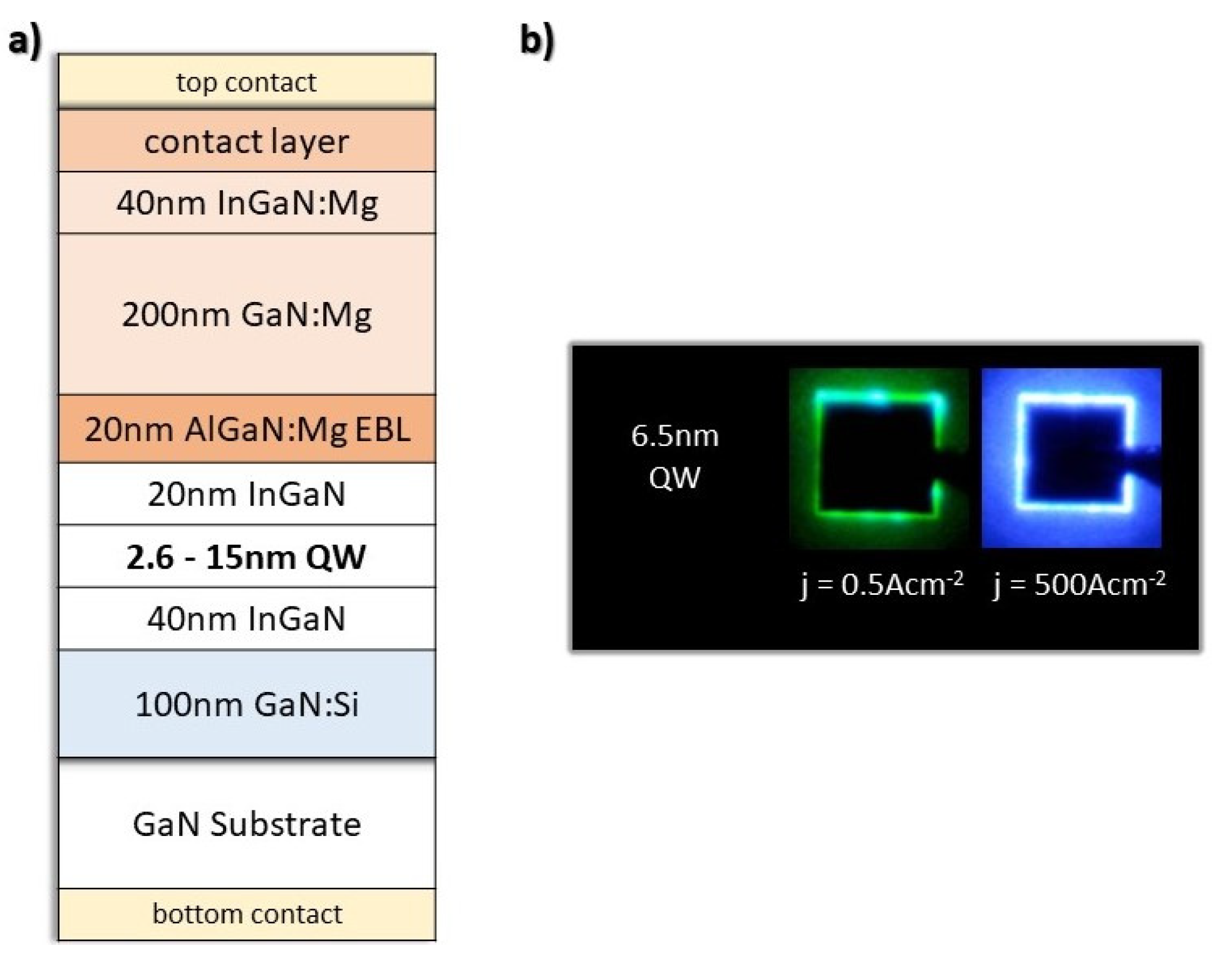
2. Samples and Methods
3. Results and Discussion
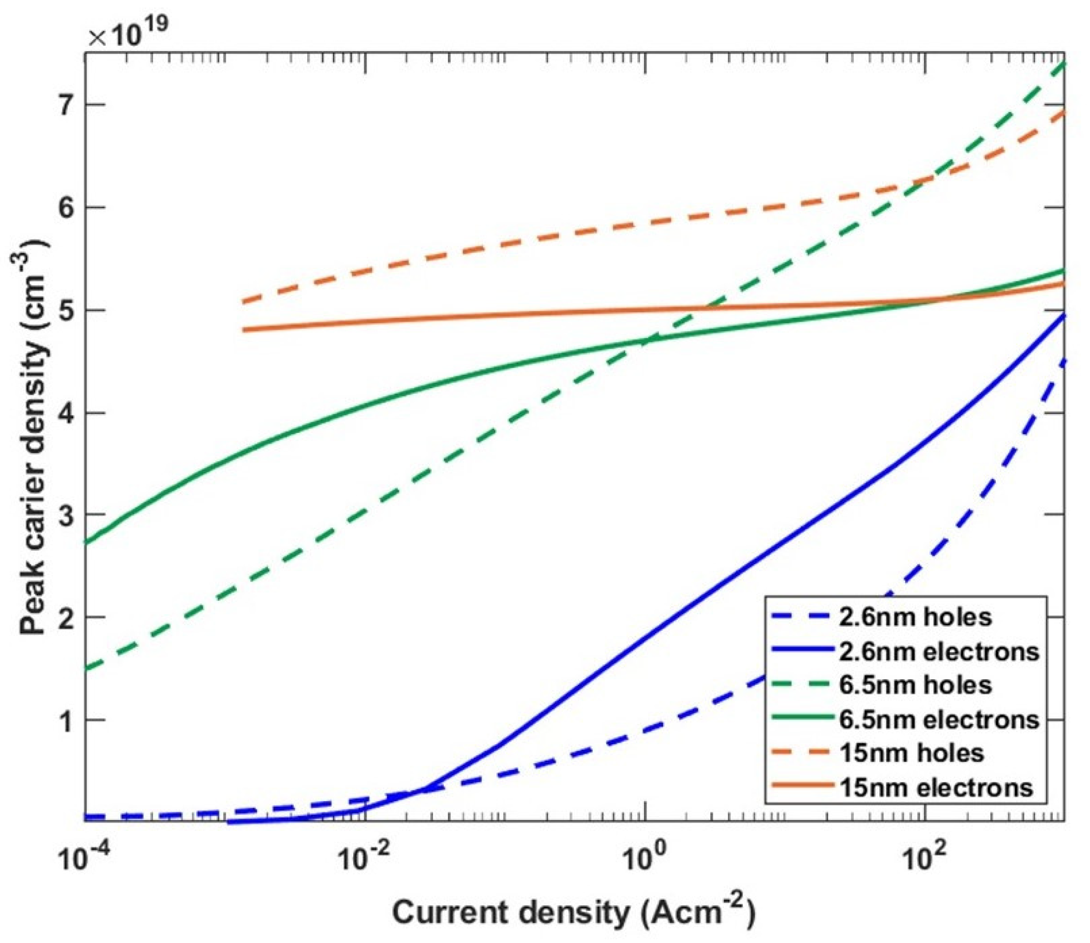
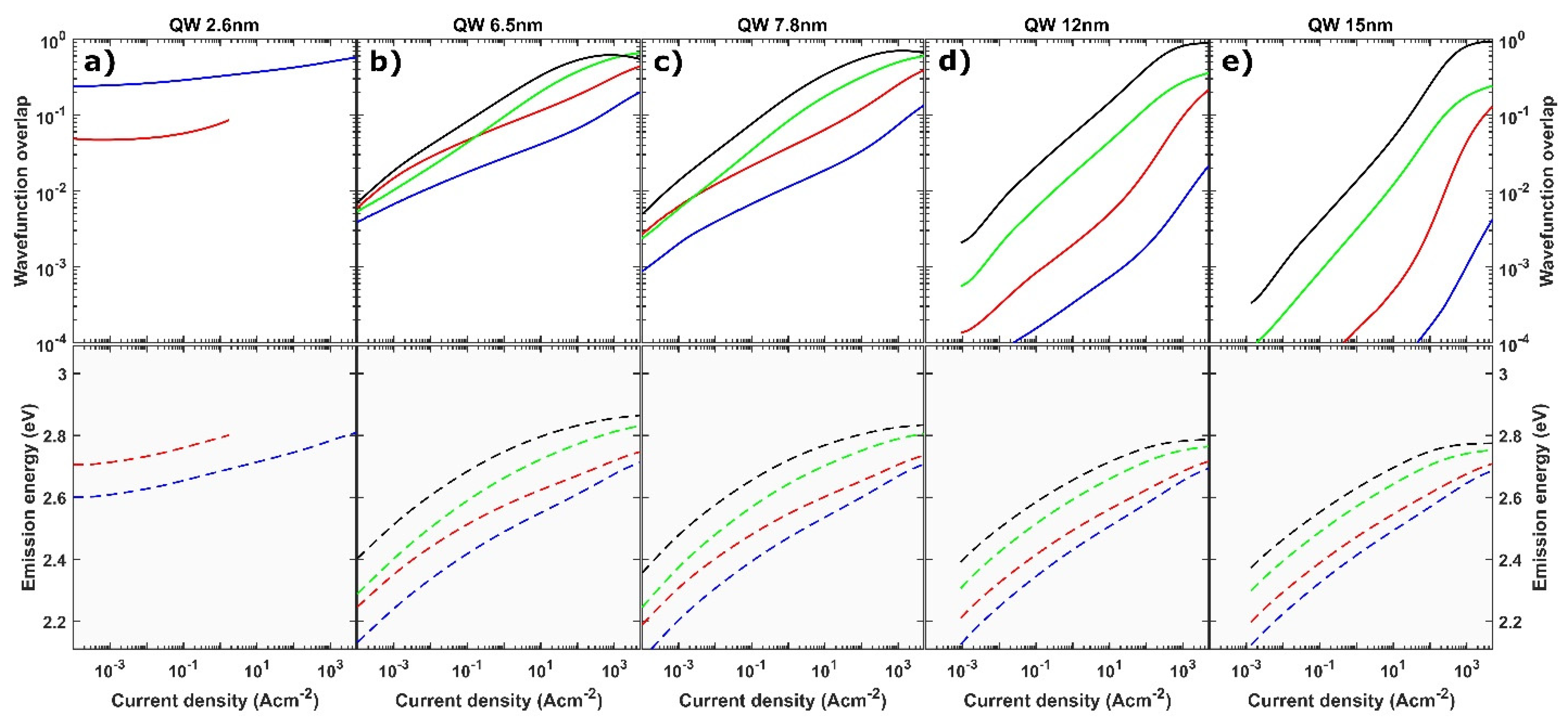
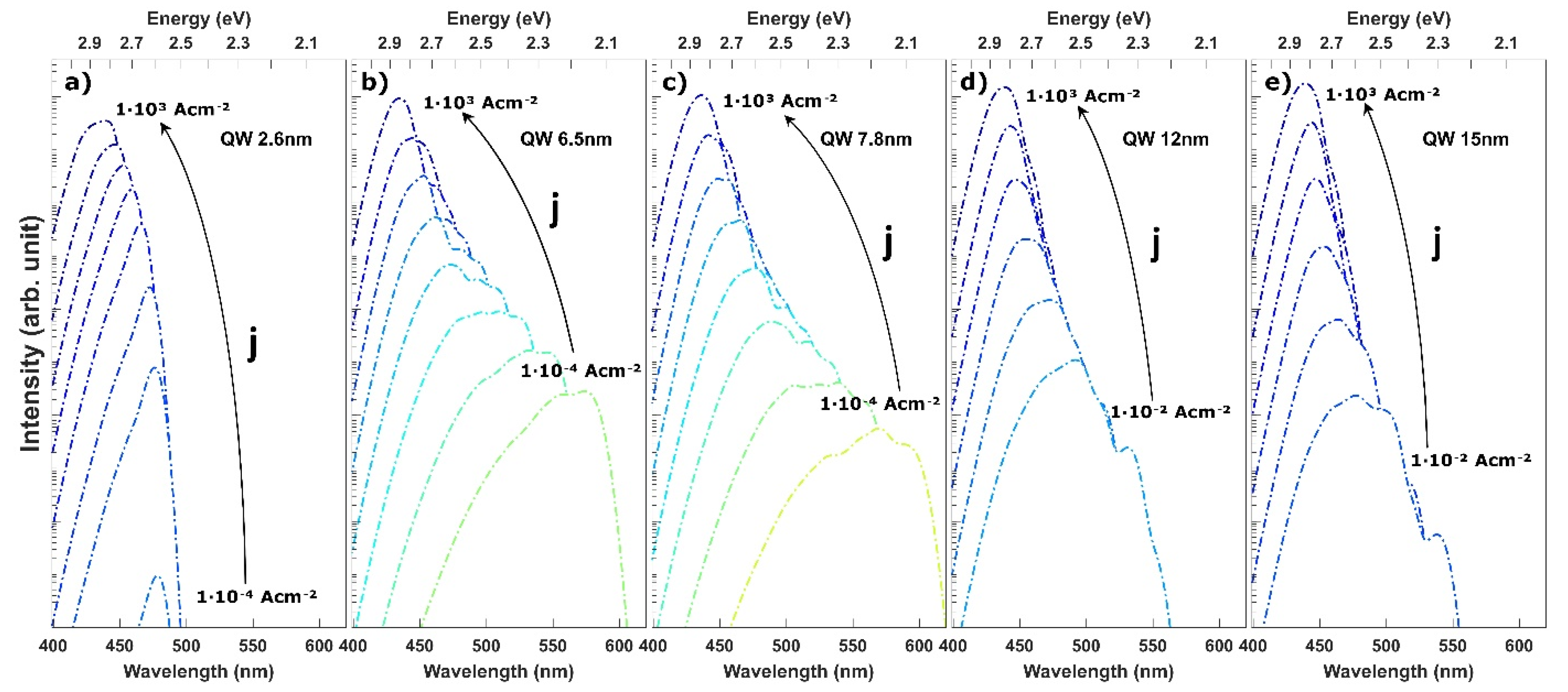
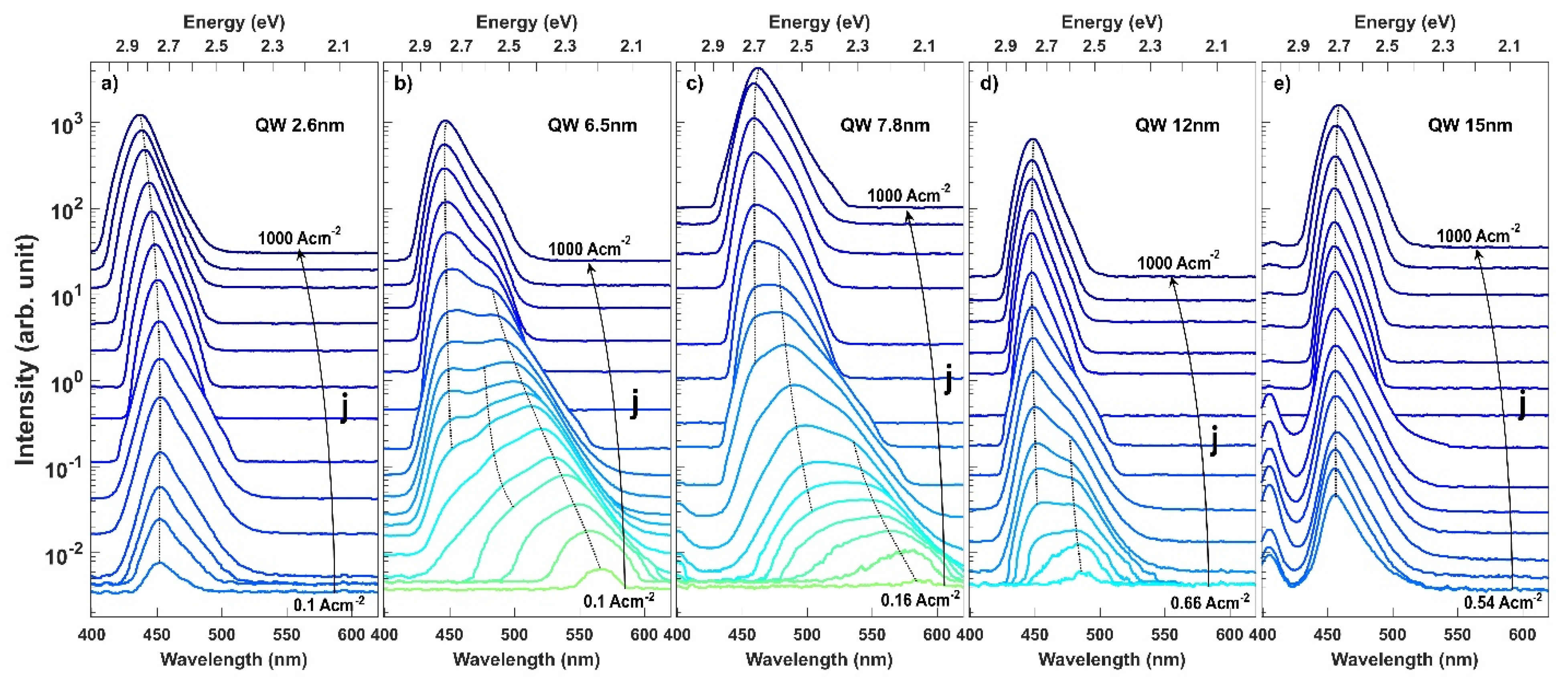
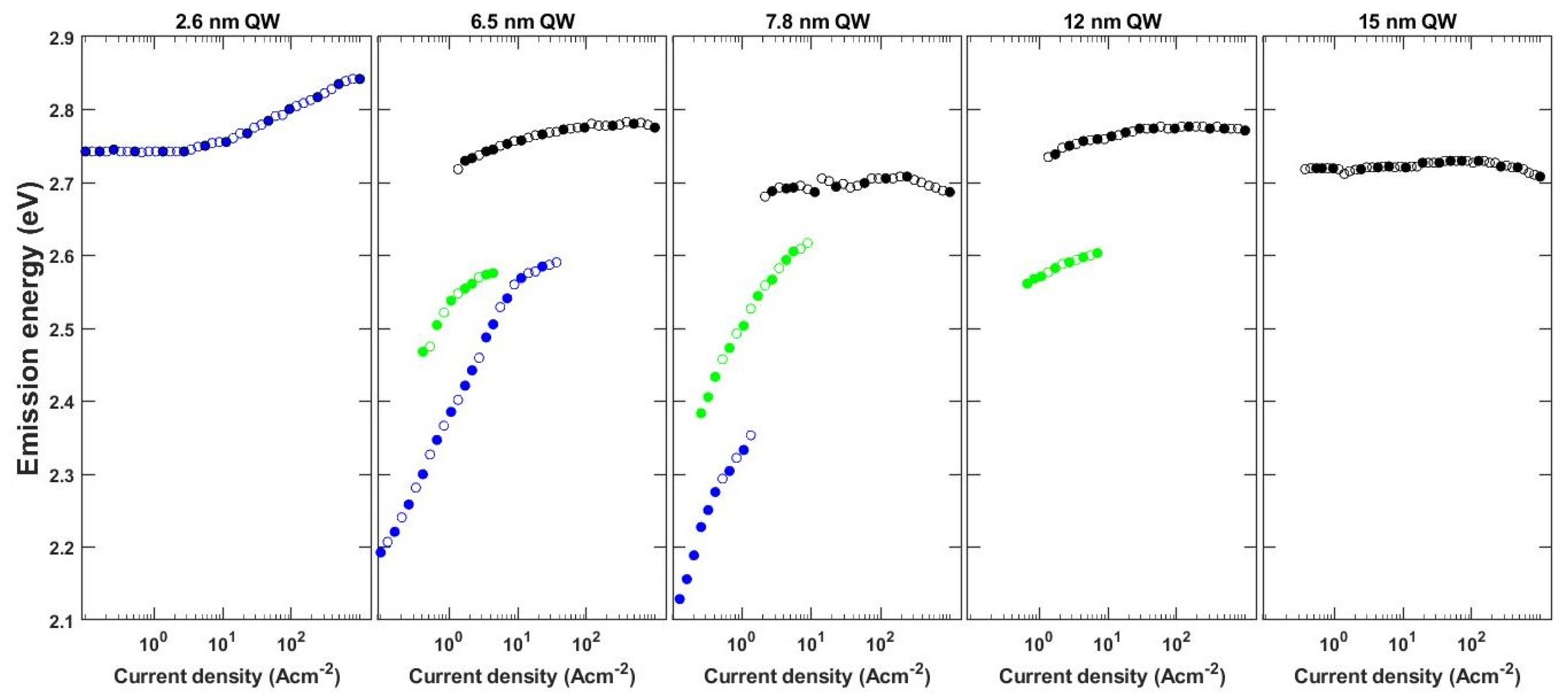
3.1. Experiment
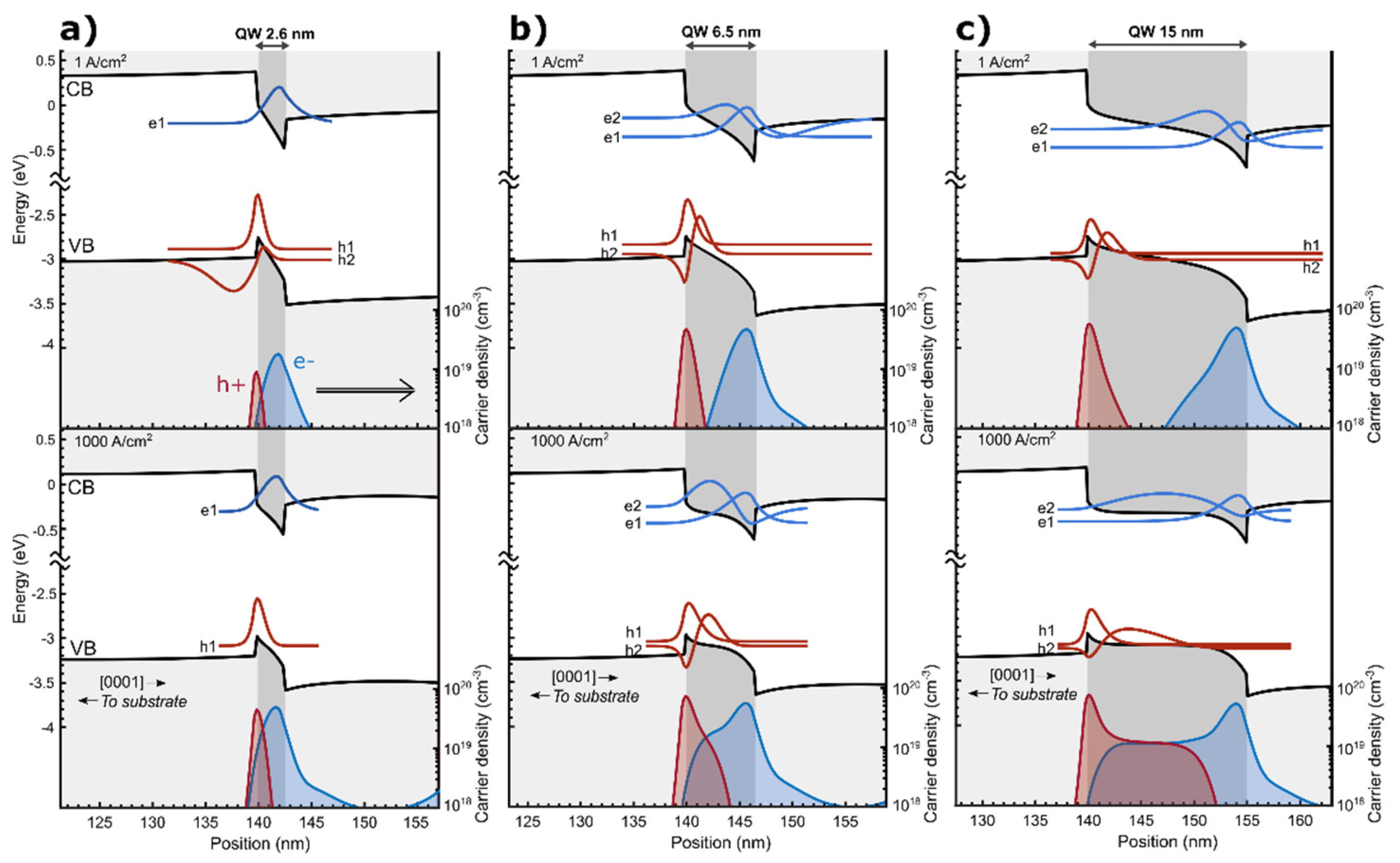
3.2. Simulation
4. Conclusions
Author Contributions
Funding
Data Availability Statement
Conflicts of Interest
References
- Haitz, R.; Tsao, J.Y. Solid-state lighting: ‘The case’ 10 years after and future prospects. Phys. Status Solidi A 2011, 208, 17–29. [Google Scholar] [CrossRef]
- DenBaars, S.P.; Feezell, D.; Kelchner, K.; Pimputkar, S.; Pan, C.; Yen, C.; Tanaka, S.; Zhao, Y.; Pfaff, N.; Farrell, R.; et al. Development of gallium-nitride-based light-emitting diodes (LEDs)and laser diodes for energy-efficient lighting and displays. Acta Mater. 2013, 61, 945–951. [Google Scholar] [CrossRef]
- Wierer, J.J.; Tsao, J.Y.; Sizov, D.S. Comparison between blue lasers and light-emitting diodes for future solid-state lighting. Laser Photon. Rev. 2013, 7, 963. [Google Scholar] [CrossRef]
- Hurni, C.A.; David, A.; Cich, M.J.; Aldaz, R.I.; Ellis, B.; Huang, K.; Tyagi, A.; DeLille, R.A.; Craven, M.D.; Steranka, F.M.; et al. Bulk GaN flip-chip violet light-emitting diodes with optimized efficiency for high-power operation. Appl. Phys. Lett. 2015, 106, 031101. [Google Scholar] [CrossRef]
- David, A.; Hurni, C.A.; Aldaz, R.I.; Cich, M.J.; Ellis, B.; Huang, K.; Steranka, F.M.; Krames, M.R. High light extraction efficiency in bulk-GaN based volumetric violet light-emitting diodes. Appl. Phys. Lett. 2014, 105, 231111. [Google Scholar] [CrossRef]
- Zhou, S.; Liu, X.; Yan, H.; Chen, Z.; Liu, Y.; Liu, S. Highly efficient GaN-based high-power flipchip light-emitting diodes. Opt. Express 2019, 27, A669. [Google Scholar] [CrossRef]
- Bernardini, F.; Fiorentini, V.; Vanderbilt, D. Spontaneous polarization and piezoelectric constants of III-V nitrides. Phys. Rev. B 1997, 56, R10024–R10027. [Google Scholar] [CrossRef] [Green Version]
- Ambacher, O.; Smart, J.; Shealy, J.R.; Weimann, N.G.; Chu, K.; Murphy, M.; Schaff, W.J.; Eastman, L.F.; Dimitrov, R.; Wittmer, L.; et al. Two-dimensional electron gases induced by spontaneous and piezoelectric polarization charges in N- and Ga-face AlGaN/GaN heterostructures. J. Appl. Phys. 1999, 85, 3222. [Google Scholar] [CrossRef] [Green Version]
- Cordier, Y.; Hugues, M.; Lorenzini, P.; Semond, F.; Natali, F.; Massies, J. Electron mobility and transfer characteristics in AlGaN/GaN HEMTs. Phys. Status Solidi C 2005, 2, 2720–2723. [Google Scholar] [CrossRef]
- Żak, M.; Muziol, G.; Turski, H.; Siekacz, M.; Nowakowski-Szkudlarek, K.; Feduniewicz-Żmuda, A.; Chlipała, M.; Lachowski, A.; Skierbiszewski, C. Tunnel Junctions with a Doped (In, Ga)N Quantum Well for Vertical Integration of III-Nitride Optoelectronic Devices. Phys. Rev. Appl. 2021, 15, 024046. [Google Scholar] [CrossRef]
- Krishnamoorthy, S.; Nath, D.N.; Akyol, F.; Park, P.S.; Esposto, M.; Rajan, S. Polarization-engineered GaN/InGaN/GaN tunnel diodes. Appl. Phys. Lett. 2010, 97, 203502. [Google Scholar] [CrossRef] [Green Version]
- Simon, J.; Zhang, Z.; Goodman, K.; Xing, H.; Kosel, T.; Fay, P.; Jena, D. Polarization-Induced Zener Tunnel Junctions in Wide-Band-Gap Heterostructures. Phys. Rev. Lett. 2009, 103, 026801. [Google Scholar] [CrossRef] [PubMed]
- Turski, H.; Siekacz, M.; Muzioł, G.; Hajdel, M.; Stańczyk, S.; Żak, M.; Chlipała, M.; Skierbiszewski, C.; Bharadwaj, S.; Xing, H.G. Nitride LEDs and lasers with buried tunnel junctions. ECS J. Solid State Sci. Technol. 2020, 9, 015018. [Google Scholar] [CrossRef]
- Chlipala, M.; Turski, H.; Siekacz, M.; Pieniak, K.; Nowakowski-Szkudlarek, K.; Suski, T.; Skierbiszewski, C. Nitride light-emitting diodes for cryogenic temperatures. Opt. Express 2020, 28, 30299–30308. [Google Scholar] [CrossRef]
- Zhang, Y.; Kao, T.; Liu, J.; Lochner, Z.; Kim, S.; Ryou, J.; Dupuis, R.D.; Shen, S. Effects of a stepgraded AlxGa1−xN electron blocking layer in InGaN-based laser diodes. J. Appl. Phys. 2011, 109, 083115. [Google Scholar] [CrossRef]
- Simon, J.; Protasenko, V.; Lian, C.; Xing, H.; Jena, D. Polarization-Induced Hole Doping in Wide–Band- Gap Uniaxial Semiconductor Heterostructures. Science 2010, 327, 60–64. [Google Scholar] [CrossRef] [PubMed] [Green Version]
- Yan, L.; Zhang, Y.; Han, X.; Deng, G.; Li, P.; Yu, Y.; Chen, L.; Li, X.; Song, J. Polarization-induced hole doping in N-polar III-nitride LED grown by metalorganic chemical vapor deposition. Appl. Phys. Lett. 2018, 112, 182104. [Google Scholar] [CrossRef] [Green Version]
- Aumer, M.E.; LeBoeuf, S.F.; Moody, B.F.; Bedair, S.M. Strain-induced piezoelectric field effects on light emission energy and intensity from AlInGaN/InGaN quantum wells. Appl. Phys. Lett. 2001, 79, 3803. [Google Scholar] [CrossRef]
- Kafar, A.; Stanczyk, S.; Grzanka, S.; Pieniak, K.; Suski, T.; Perlin, P. Screening of quantum-confined Stark effect in nitride laser diodes and superluminescent diodes. Appl. Phys. Express 2019, 12, 044001. [Google Scholar] [CrossRef]
- Della Sala, F.; di Carlo, A.; Lugli, P.; Bernardini, F.; Fiorentini, V.; Scholz, R.; Jancu, J.-M. Free-carrier screening of polarization fields in wurtzite GaN/InGaN laser structures. Appl. Phys. Lett. 1999, 74, 2002–2004. [Google Scholar] [CrossRef] [Green Version]
- Young, N.G.; Farrell, R.M.; Oh, S.; Cantore, M.; Wu, F.; Nakamura, S.; DenBaars, S.P.; Weisbuch, C.; Speck, J.S. Polarization field screening in thick (0001) InGaN/GaN single quantum well light-emitting diodes. Appl. Phys. Lett. 2016, 108, 061105. [Google Scholar] [CrossRef]
- Bai, J.; Wang, T.; Sakai, S. Influence of the quantum-well thickness on the radiative recombination of InGaN/GaN quantum well structures. J. Appl. Phys. 2000, 88, 4729–4733. [Google Scholar] [CrossRef]
- Damilano, B.; Grandjean, N.; Massies, J.; Siozade, L.; Leymarie, J. InGaN/GaN quantum wells grown by molecular-beam epitaxy emitting from blue to red at 300 K. Appl. Phys. Lett. 2000, 77, 1268–1270. [Google Scholar] [CrossRef]
- Arif, R.A.; Ee, Y.-K.; Tansu, N. Polarization engineering via staggered InGaN quantum wells for radiative efficiency enhancement of light emitting diodes. Appl. Phys. Lett. 2007, 91, 091110. [Google Scholar] [CrossRef] [Green Version]
- Zhao, X.; Tang, B.; Gong, L.; Bai, J.; Ping, J.; Zhou, S. Rational construction of staggered InGaN quantum wells for efficient yellow light-emitting diodes. Appl. Phys. Lett. 2021, 118, 182102. [Google Scholar] [CrossRef]
- Gardner, N.F.; Müller, G.O.; Shen, Y.C.; Chen, G.; Watanabe, S.; Götz, W.; Krames, M.R. Blue-emitting InGaN–GaN double-heterostructure light-emitting diodes reaching maximum quantum efficiency above 200A∕cm2. Appl. Phys. Lett. 2007, 91, 243506. [Google Scholar] [CrossRef]
- Laubsch, A.; Bergbauer, W.; Sabathil, M.; Strassburg, M.; Lugauer, H.; Peter, M.; Meyer, T.; Bruderl, G.; Wagner, J.; Linder, N.; et al. Luminescence properties of thick InGaN quantum-wells. Phys. Status Solidi C 2009, 6, S885–S888. [Google Scholar] [CrossRef]
- Kawaguchi, M.; Imafuji, O.; Nozaki, S.; Hagino, H.; Takigawa, S.; Katayama, T.; Tanaka, T. Optical-loss suppressed InGaN laser diodes using undoped thick waveguide structure. In Proceedings of the SPIE 9748, Gallium Nitride Materials and Devices XI, San Francisco, CA, USA, 13–18 February 2016; p. 974818. [Google Scholar] [CrossRef]
- Zhang, Z.; Kushimoto, M.; Sakai, T.; Sugiyama, N.; Schowalter, L.J.; Sasaoka, C.; Amano, H. A 271.8 nm deep-ultraviolet laser diode for room temperature operation. Appl. Phys. Express 2019, 12, 124003. [Google Scholar] [CrossRef]
- Muziol, G.; Turski, H.; Siekacz, M.; Szkudlarek, K.; Janicki, L.; Baranowski, M.; Zolud, S.; Kudrawiec, R.; Suski, T.; Skierbiszewski, C. Beyond Quantum Efficiency Limitations Originating from the Piezoelectric Polarization in Light-Emitting Devices. ACS Photonics 2019, 6, 1963–1971. [Google Scholar] [CrossRef]
- Muziol, G.; Hajdel, M.; Siekacz, M.; Szkudlarek, K.; Stanczyk, S.; Turski, H.; Skierbiszewski, C. Optical properties of III-nitride laser diodes with wide InGaN quantum wells. Appl. Phys. Express 2019, 12, 072003. [Google Scholar] [CrossRef]
- Bercha, A.; Trzeciakowski, W.; Muzioł, G.; Siekacz, M.; Skierbiszewski, C. Anomalous photocurrent in wide InGaN quantum wells. Opt. Express 2020, 28, 4717–4725. [Google Scholar] [CrossRef] [PubMed]
- Pieniak, K.; Chlipala, M.; Turski, H.; Trzeciakowski, W.; Muziol, G.; Staszczak, G.; Kafar, A.; Makarowa, I.; Grzanka, E.; Grzanka, S.; et al. Quantum-confined Stark effect and mechanisms of its screening in InGaN/GaN light-emitting diodes with a tunnel junction. Opt. Express 2021, 29, 1824–1837. [Google Scholar] [CrossRef]
- Turski, H.; Muziol, G.; Wolny, P.; Grzanka, S.; Cywiński, G.; Sawicka, M.; Perlin, P.; Skierbiszewski, C. Cyan laser diode grown by plasma-assisted molecular beam epitaxy. Appl. Phys. Lett. 2014, 104, 023503. [Google Scholar] [CrossRef]
- Skierbiszewski, C.; Turski, H.; Muziol, G.; Siekacz, M.; Sawicka, M.; Cywiński, G.; Wasilewski, Z.R.; Porowski, S. Nitride-based laser diodes grown by plasma-assisted molecular beam epitaxy. J. Phys. D Appl. Phys. 2014, 47, 073001. [Google Scholar] [CrossRef]
- Turski, H.; Siekacz, M.; Wasilewski, Z.R.; Sawicka, M.; Porowski, S.; Skierbiszewski, C. Nonequivalent atomic step edges—Role of gallium and nitrogen atoms in the growth of InGaN layers. J. Cryst. Growth 2013, 367, 115–121. [Google Scholar] [CrossRef]
- Wu, Y.; Chiu, C.; Chang, C.; Yu, P.; Kuo, H. Size-Dependent Strain Relaxation and Optical Characteristics of InGaN/GaN Nanorod LEDs. IEEE J. Sel. Top. Quantum Electron. 2009, 15, 1226–1233. [Google Scholar] [CrossRef]
- Wu, Y.; Singh, J. Metal piezoelectric semiconductor field effect transistors for piezoelectric strain sensors. Appl. Phys. Lett. 2004, 85, 1223–1225. [Google Scholar] [CrossRef] [Green Version]
- Wu, Y.; Singh, M.; Singh, J. Gate leakage suppression and contact engineering in nitride heterostructures. J. Appl. Phys. 2003, 94, 5826–5831. [Google Scholar] [CrossRef] [Green Version]
- Muziol, G.; Hajdel, M.; Turski, H.; Nomoto, K.; Siekacz, M.; Nowakowski-Szkudlarek, K.; Żak, M.; Jena, D.; Xing, H.G.; Perlin, P.; et al. Distributed-feedback blue laser diode utilizing a tunnel junction grown by plasma-assisted molecular beam epitaxy. Opt. Express 2020, 28, 35321–35329. [Google Scholar] [CrossRef]


Publisher’s Note: MDPI stays neutral with regard to jurisdictional claims in published maps and institutional affiliations. |
© 2021 by the authors. Licensee MDPI, Basel, Switzerland. This article is an open access article distributed under the terms and conditions of the Creative Commons Attribution (CC BY) license (https://creativecommons.org/licenses/by/4.0/).
Share and Cite
Hajdel, M.; Chlipała, M.; Siekacz, M.; Turski, H.; Wolny, P.; Nowakowski-Szkudlarek, K.; Feduniewicz-Żmuda, A.; Skierbiszewski, C.; Muziol, G. Dependence of InGaN Quantum Well Thickness on the Nature of Optical Transitions in LEDs. Materials 2022, 15, 237. https://doi.org/10.3390/ma15010237
Hajdel M, Chlipała M, Siekacz M, Turski H, Wolny P, Nowakowski-Szkudlarek K, Feduniewicz-Żmuda A, Skierbiszewski C, Muziol G. Dependence of InGaN Quantum Well Thickness on the Nature of Optical Transitions in LEDs. Materials. 2022; 15(1):237. https://doi.org/10.3390/ma15010237
Chicago/Turabian StyleHajdel, Mateusz, Mikolaj Chlipała, Marcin Siekacz, Henryk Turski, Paweł Wolny, Krzesimir Nowakowski-Szkudlarek, Anna Feduniewicz-Żmuda, Czeslaw Skierbiszewski, and Grzegorz Muziol. 2022. "Dependence of InGaN Quantum Well Thickness on the Nature of Optical Transitions in LEDs" Materials 15, no. 1: 237. https://doi.org/10.3390/ma15010237
APA StyleHajdel, M., Chlipała, M., Siekacz, M., Turski, H., Wolny, P., Nowakowski-Szkudlarek, K., Feduniewicz-Żmuda, A., Skierbiszewski, C., & Muziol, G. (2022). Dependence of InGaN Quantum Well Thickness on the Nature of Optical Transitions in LEDs. Materials, 15(1), 237. https://doi.org/10.3390/ma15010237