
Modeling of the Point Defect Migration across the AlN/GaN Interfaces—Ab Initio Study

 , , , and
Abstract
:1. Introduction
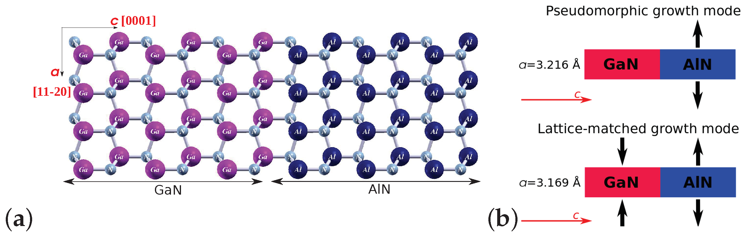
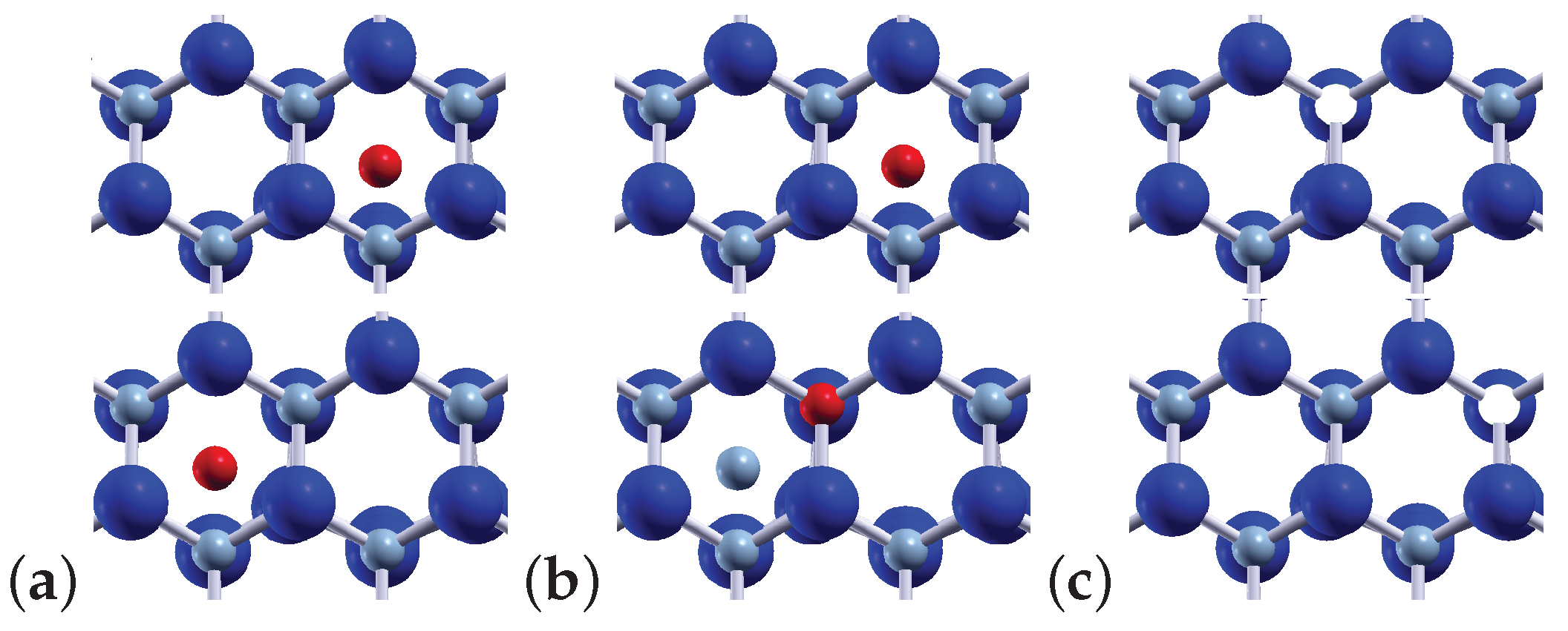
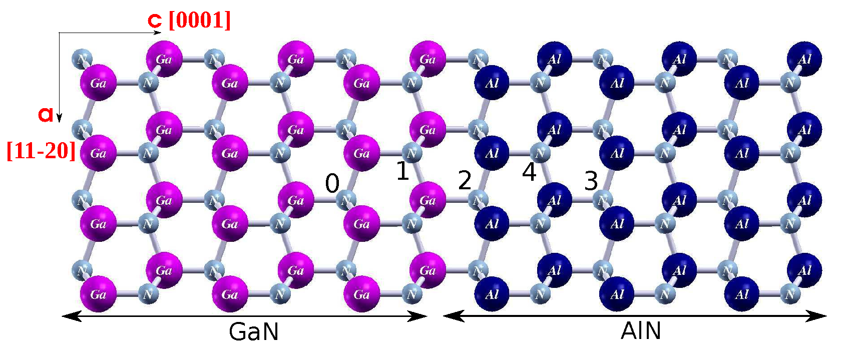
2. Models and Methods

| Property | AlN | GaN | ||
|---|---|---|---|---|
| This Paper | Exp. | This Paper | Exp. | |
| Lattice constant a (Å) | 3.124 | 3.111 [26] | 3.215 | 3.190 [26] |
| Lattice constant c (Å) | 5.013 | 4.981 [26] | 5.220 | 5.190 [26] |
| Formation enthalpy (eV) | −3.32 | −3.13 [26] | −1.34 | −1.29, −1.34 [26,27] |
3. Results
3.1. Heights of Migration Energy Barriers of Native Point Defects in Bulk GaN and AlN Crystals for Various Diffusion Mechanisms
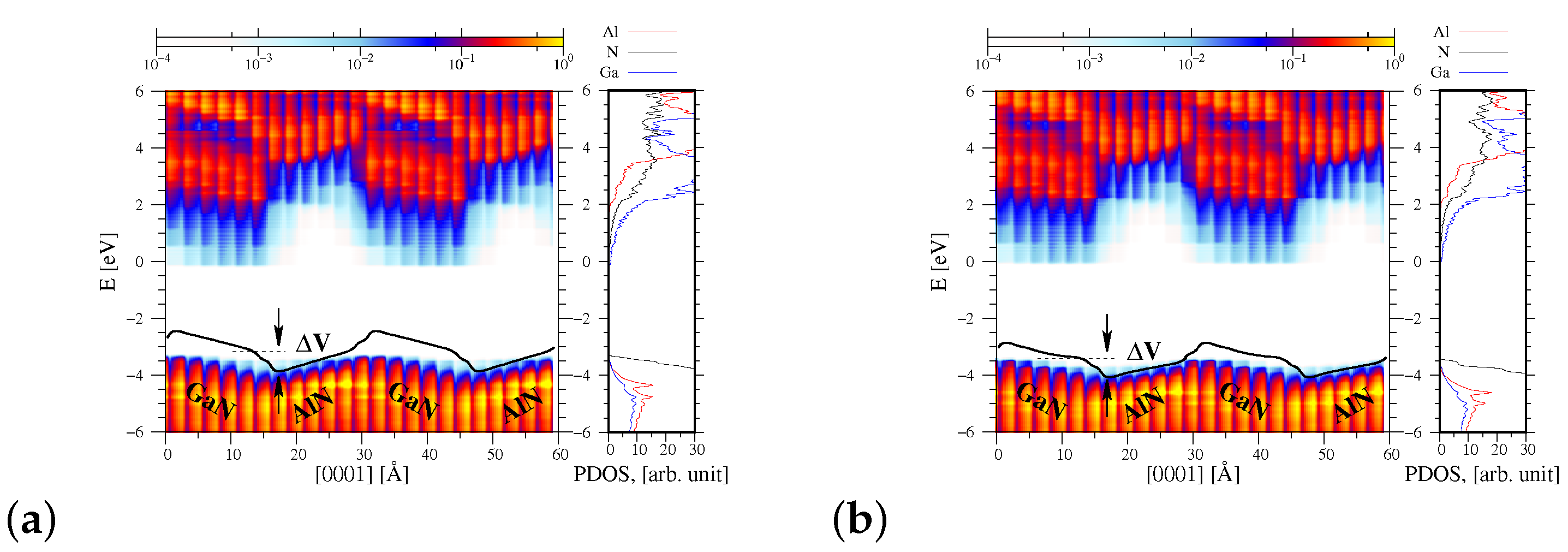
3.2. Projected DOS Function of AlN/GaN Superlattice as a Function of the Atomic Positions
4. Discussion
4.1. Diffusion of Point Defects across the AlN/GaN Strained Heterointerface Type
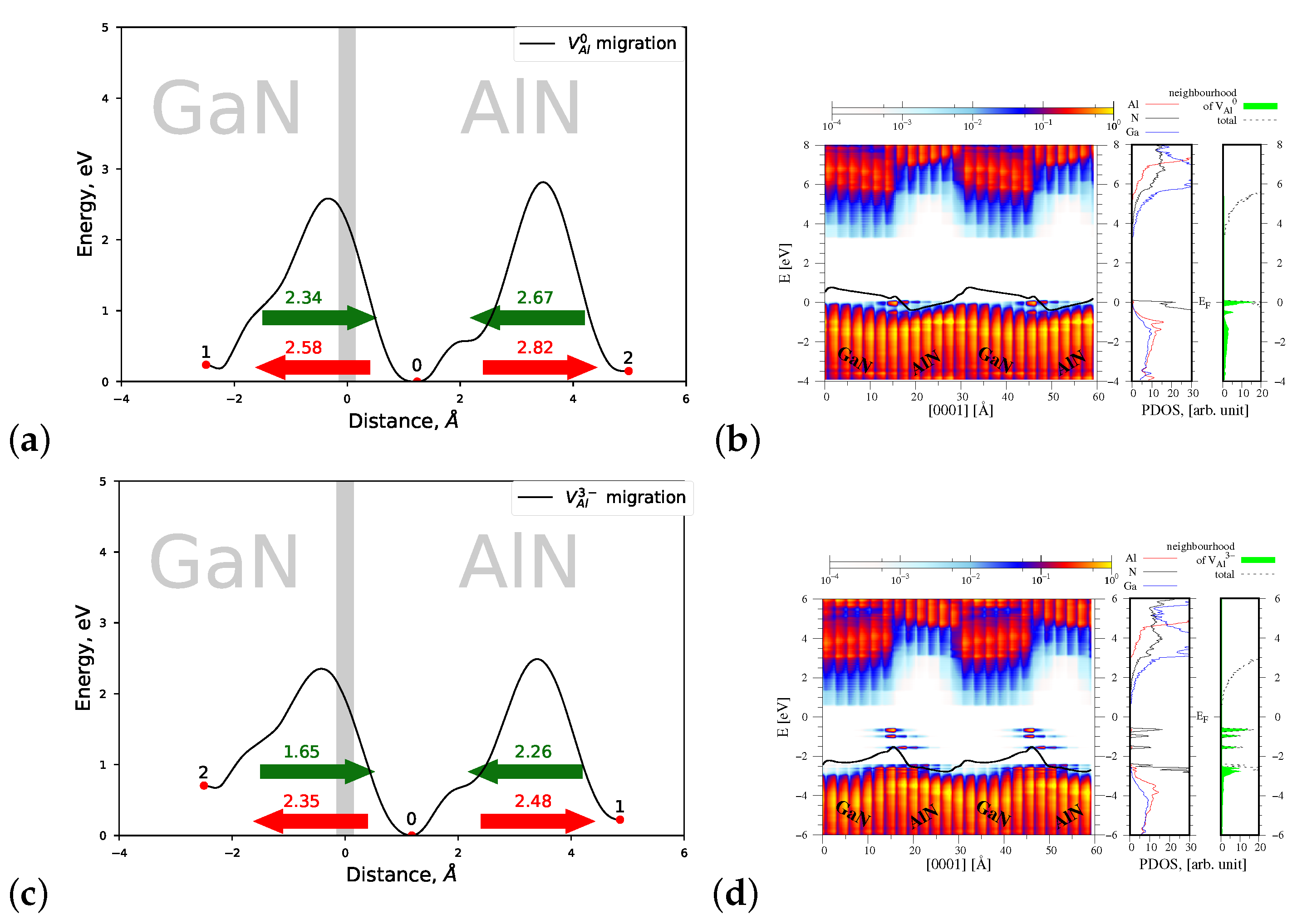
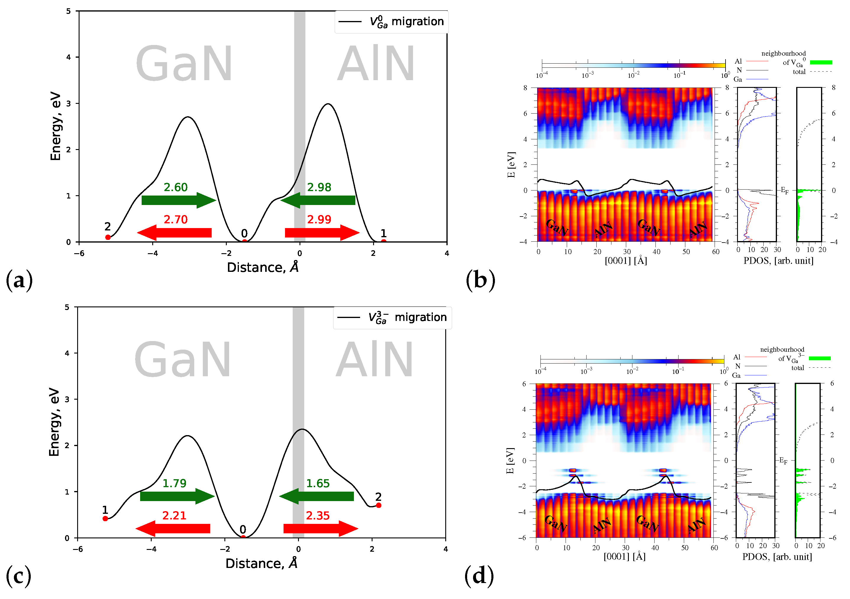
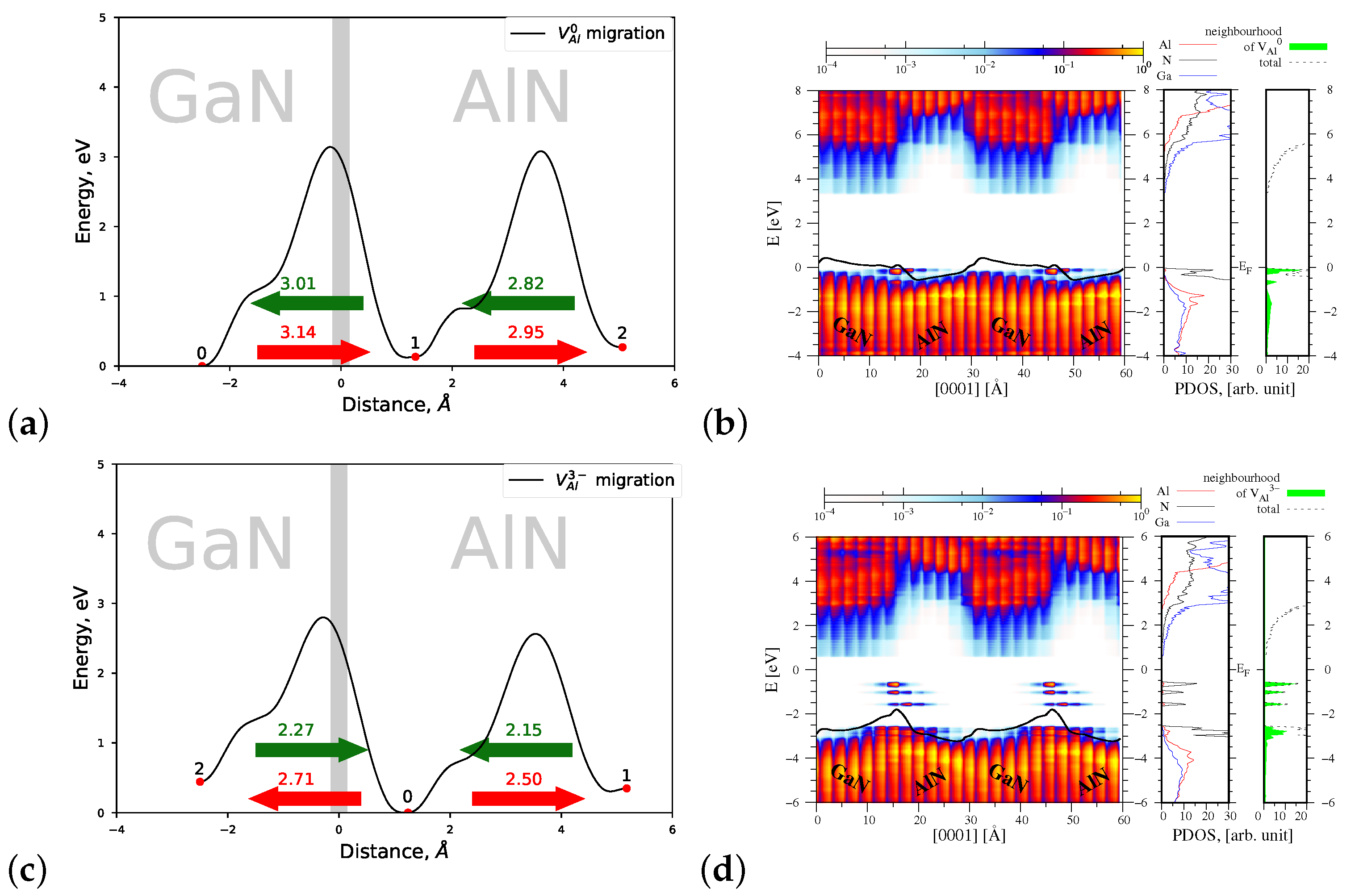
4.1.1. Migration of and
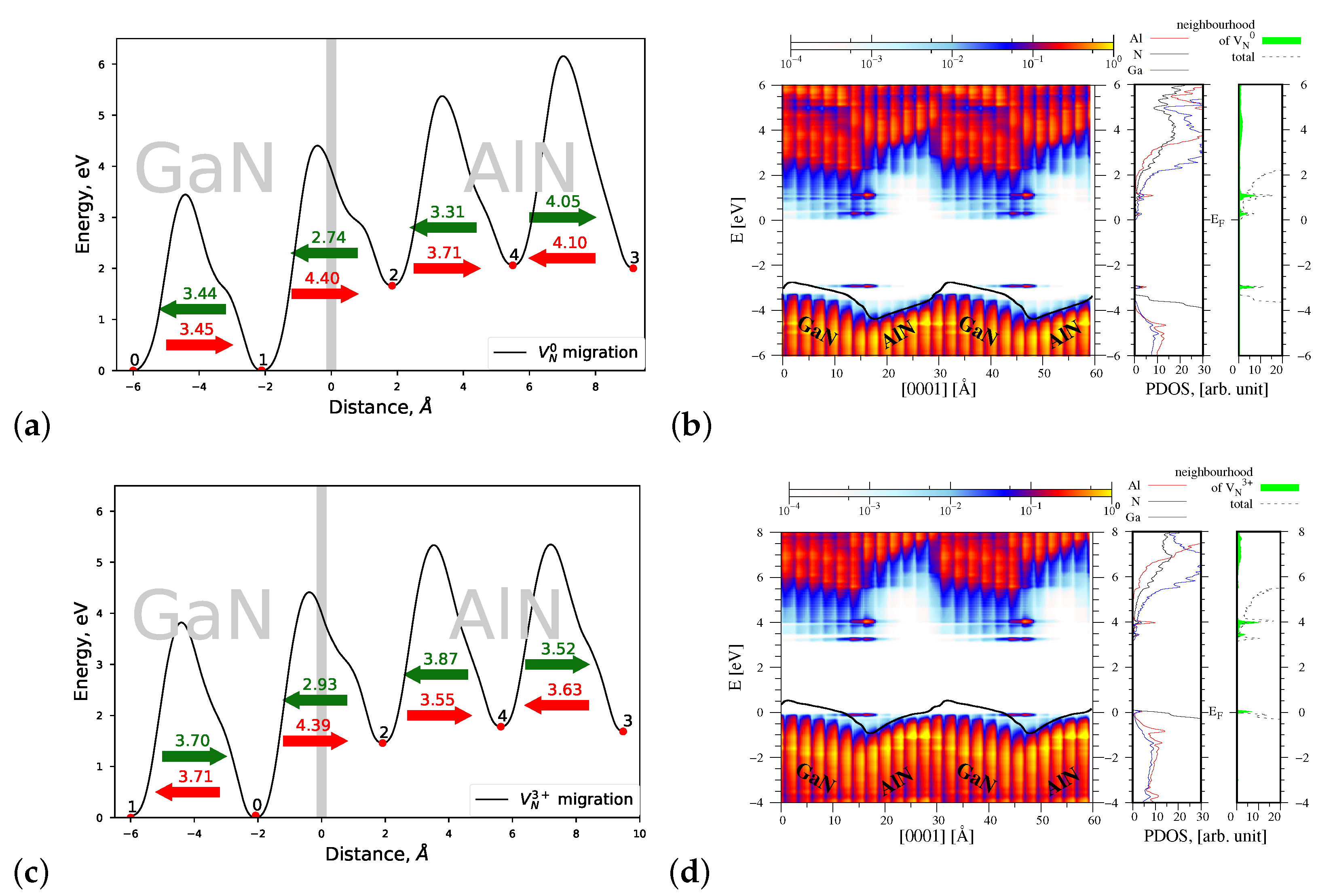
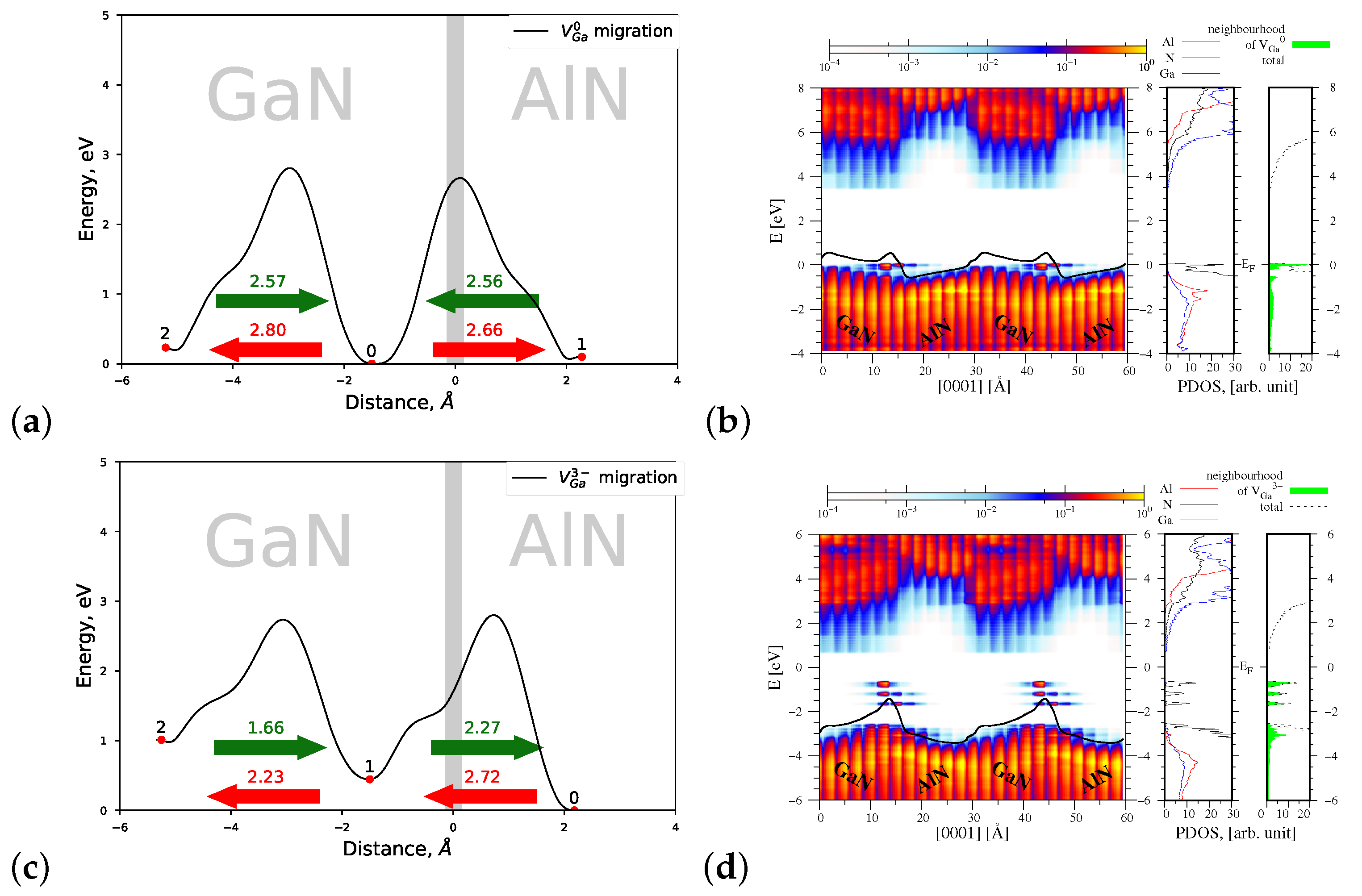
4.1.2. Migration of and
4.1.3. Migration of and
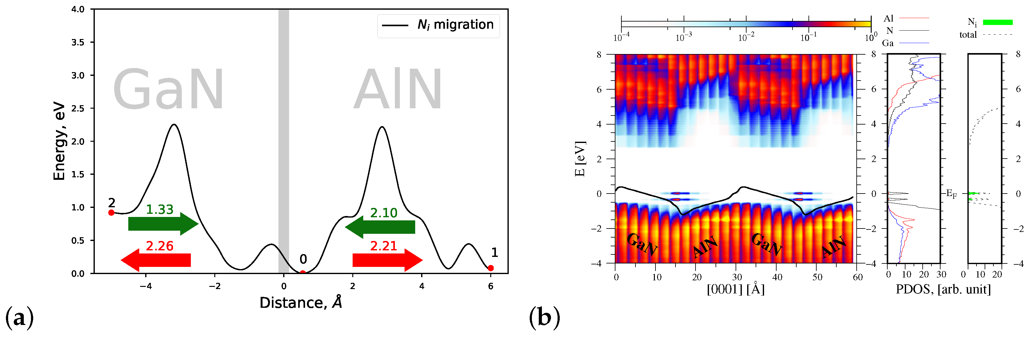
4.1.4. Migrations of and Atoms via the Indirect Diffusion Mechanism
4.2. Diffusion of Point Defects across the AlN/GaN Relaxed Interface Type
4.2.1. Migration of and
4.2.2. Migration of and
4.2.3. Migration of and
5. Conclusions
Author Contributions
Funding
Institutional Review Board Statement
Informed Consent Statement
Data Availability Statement
Acknowledgments
Conflicts of Interest
References
- Hirayama, H. Advances of AlGaN-based High-Efficiency Deep-UV LEDs. In Proceedings of the Asia Communications and Photonics Conference and Exhibition, Shanghai, China, 8–12 December 2010; pp. 641–642. [Google Scholar]
- Li, P.; Han, X.; Yan, L.; Deng, G.; Liu, M.; Zhang, Y.; Zhang, B. The preparation of different pairs near-ultraviolet AlGaN/GaN DBRs with AlN interlayer. Mater. Sci. Semicond. Process. 2018, 80, 162–166. [Google Scholar] [CrossRef]
- Han, J.; Crawford, M.; Shul, R.; Figiel, J.; Banas, M.; Zhang, L.; Song, Y.; Zhou, H.; Nurmikko, A. AlGaN/GaN quantum well ultraviolet light emitting diodes. Appl. Phys. Lett. 1998, 73, 1688–1690. [Google Scholar] [CrossRef]
- Someya, T.; Arakawa, Y. Highly reflective GaN/Al0.34Ga0.66N quarter-wave reflectors grown by metal organic chemical vapor deposition. Appl. Phys. Lett. 1998, 73, 3653–3655. [Google Scholar] [CrossRef]
- Cao, Y.; Jena, D. High-mobility window for two-dimensional electron gases at ultrathin AlN/GaN heterojunctions. Appl. Phys. Lett. 2007, 90, 182112. [Google Scholar] [CrossRef] [Green Version]
- Monemar, B.; Bergman, J.; Buyanova, I.; Amano, H.; Akasaki, I.; Detchprohm, T.; Hiramatsu, K.; Sawaki, N. The excitonic bandgap of GaN: Dependence on substrate. Solid-State Electron. 1997, 41, 239–241. [Google Scholar] [CrossRef]
- Yeo, Y.; Chong, T.; Li, M. Electronic band structures and effective-mass parameters of wurtzite GaN and InN. J. Appl. Phys. 1998, 83, 1429–1436. [Google Scholar] [CrossRef]
- Silveira, E.; Freitas, J.; Schujman, S.; Schowalter, L. AlN bandgap temperature dependence from its optical properties. J. Cryst. Growth 2008, 310, 4007–4010. [Google Scholar] [CrossRef]
- Martens, M.; Schlegel, J.; Vogt, P.; Brunner, F.; Lossy, R.; Würfl, J.; Weyers, M.; Kneissl, M. High gain ultraviolet photodetectors based on AlGaN/GaN heterostructures for optical switching. Appl. Phys. Lett. 2011, 98, 211114. [Google Scholar] [CrossRef]
- Nakamura, S.; Mukai, T.; Senoh, M. Candela-class high-brightness InGaN/AlGaN double-heterostructure blue-light-emitting diodes. Appl. Phys. Lett. 1994, 64, 1687–1689. [Google Scholar] [CrossRef]
- Allerman, A.; Crawford, M.; Fischer, A.; Bogart, K.; Lee, S.; Follstaedt, D.; Provencio, P.; Koleske, D. Growth and design of deep-UV (240–290 nm) light emitting diodes using AlGaN alloys. J. Cryst. Growth 2004, 272, 227–241. [Google Scholar] [CrossRef]
- Cai, D.; Chen, X.; Xu, H.; Lin, N.; Xu, F.; Chen, H. Abruptness Improvement of the Interfaces of AlGaN/GaN Superlattices by Cancelling Asymmetric Diffusion. Jpn. J. Appl. Phys. 2013, 52, 08JB30. [Google Scholar] [CrossRef]
- Chaaben, N.; Laifi, J.; Bouazizi, H.; Saidi, C.; Bchetnia, A.; El Jani, B. Study of Al diffusion in GaN during metal organic vapor phase epitaxy of AlGaN/GaN and AlN/GaN structures. Mater. Sci. Semicond. Process. 2016, 42, 359–363. [Google Scholar] [CrossRef]
- Kim, H.; Yun, H.J.; Choi, S.; Choi, B.J. Interface trap characterization of AlN/GaN heterostructure with Al2O3, HfO2, and HfO2/Al2O3 dielectrics. J. Vac. Sci. Technol. B 2019, 37, 041203. [Google Scholar] [CrossRef]
- Aleksandrov, I.A.; Malin, T.V.; Zhuravlev, K.S.; Trubina, S.V.; Erenburg, S.B.; Pecz, B.; Lebiadok, Y.V. Diffusion in GaN/AlN superlattices: DFT and EXAFS study. Appl. Surf. Sci. 2020, 515, 146001. [Google Scholar] [CrossRef]
- Gao, Y.; Sun, D.; Jiang, X.; Zhao, J. Ab initio analytic calculation of point defects in AlGaN/GaN heterointerfaces. J. Condens. Matter Phys. 2021, 33, 035002. [Google Scholar] [CrossRef] [PubMed]
- Strak, P.; Kempisty, P.; Ptasinska, M.; Krukowski, S. Principal physical properties of GaN/AlN multiquantum well systems determined by density functional theory calculations. J. Appl. Phys. 2013, 113, 193706. [Google Scholar] [CrossRef]
- Kaminska, A.; Strak, P.; Borysiuk, J.; Sobczak, K.; Domagala, J.; Beeler, M.; Grzanka, E.; Sakowski, K.; Krukowski, S.; Monroy, E. Correlation of optical and structural properties of GaN/AlN multi-quantum wells—Ab initio and experimental study. J. Appl. Phys. 2016, 119, 015703. [Google Scholar] [CrossRef]
- Strak, P.; Kempisty, P.; Sakowski, K.; Kaminska, A.; Jankowski, D.; Korona, K.P.; Sobczak, K.; Borysiuk, J.; Beeler, M.; Grzanka, E.; et al. Ab initio and experimental studies of polarization and polarization related fields in nitrides and nitride structures. AIP Adv. 2017, 7, 015027. [Google Scholar] [CrossRef] [Green Version]
- Ordejón, P.; Artacho, E.; Soler, J.M. Self-consistent order density-functional calculations for very large systems. Phys. Rev. B Condens. Matter Mater. Phys. 1996, 53, R10441–R10444. [Google Scholar] [CrossRef] [Green Version]
- Soler, J.M.; Artacho, E.; Gale, J.D.; García, A.; Junquera, J.; Ordejón, P.; Sánchez-Portal, D. The SIESTA method for ab initio order-N materials simulation. J. Condens. Matter Phys. 2002, 14, 2745–2779. [Google Scholar] [CrossRef] [Green Version]
- Perdew, J.P.; Burke, K.; Ernzerhof, M. Generalized gradient approximation made simple. Phys. Rev. Lett. 1996, 77, 3865–3868. [Google Scholar] [CrossRef] [Green Version]
- Odashima, M.M.; Capelle, K.; Trickey, S.B. Tightened lieb-oxford bound for systems of fixed particle number. J. Chem. Theory Comput. 2009, 5, 798–807. [Google Scholar] [CrossRef] [Green Version]
- Pedroza, L.S.; Da Silva, A.J.; Capelle, K. Gradient-dependent density functionals of the Perdew-Burke-Ernzerhof type for atoms, molecules, and solids. Phys. Rev. B Condens. Matter Mater. Phys. 2009, 79, 201106. [Google Scholar] [CrossRef] [Green Version]
- Hrytsak, R.; Kempisty, P.; Grzanka, E.; Leszczynski, M.; Sznajder, M. DFT study on point defects migration through the pseudomorphic and lattice-matched InN/GaN interfaces. Comput. Mater. Sci. 2021, 186, 110039. [Google Scholar] [CrossRef]
- Madelung, O. (Ed.) Semiconductors—Basic Data; Springer: Berlin/Heidelberg, Germany, 1996; p. 317. [Google Scholar]
- Jacob, K.T.; Rajitha, G. Discussion of enthalpy, entropy and free energy of formation of GaN. J. Cryst. Growth 2009, 311, 3806–3810. [Google Scholar] [CrossRef]
- Mehrer, H. Diffusion in Solids: Fundamentals, Methods, Materials, Diffusion-Controlled Processes; Springer: Berlin/Heidelberg, Germany, 2007; pp. 95–104. [Google Scholar]
- Warnick, K.H.; Puzyrev, Y.; Roy, T.; Fleetwood, D.M.; Schrimpf, R.D.; Pantelides, S.T. Room-temperature diffusive phenomena in semiconductors: The case of AlGaN. Phys. Rev. B Condens. Matter Mater. Phys. 2011, 84, 214109. [Google Scholar] [CrossRef]
- Jónsson, H.; Mills, G.; Jacobsen, K.W. Nudged elastic band method for finding minimum energy paths of transitions. Class. Quantum Dyn. Condens. Phase Simul. 1998, 1998, 385–404. [Google Scholar]
- Henkelman, G.; Jónsson, H. Improved tangent estimate in the nudged elastic band method for finding minimum energy paths and saddle points. J. Chem. Phys. 2000, 113, 9978–9985. [Google Scholar] [CrossRef] [Green Version]
- Henkelman, G.; Uberuaga, B.P.; Jónsson, H. Climbing image nudged elastic band method for finding saddle points and minimum energy paths. J. Chem. Phys. 2000, 113, 9901–9904. [Google Scholar] [CrossRef] [Green Version]
- Stampfl, C.; Van de Walle, C. Theoretical investigation of native defects, impurities, and complexes in aluminum nitride. Phys. Rev. B 2002, 65, 155212. [Google Scholar] [CrossRef] [Green Version]
- Lyons, J.L.; Van de Walle, C.G. Computationally predicted energies and properties of defects in GaN. NPJ Comput. Mater. 2017, 3, 1–10. [Google Scholar] [CrossRef]
- Gao, Y.; Sun, D.; Jiang, X.; Zhao, J. Point defects in group III nitrides: A comparative first-principles study. J. Appl. Phys. 2019, 125, 215705. [Google Scholar] [CrossRef]
- Lyons, J.; Janotti, A.; Van de Walle, C. Effects of carbon on the electrical and optical properties of InN, GaN, and AlN. Phys. Rev. B 2014, 89, 035204. [Google Scholar] [CrossRef]
- Varley, J.; Janotti, A.; Van de Walle, C. Defects in AlN as candidates for solid-state qubits. Phys. Rev. B 2016, 93, 161201. [Google Scholar] [CrossRef] [Green Version]
- Kyrtsos, A.; Matsubara, M.; Bellotti, E. Migration mechanisms and diffusion barriers of carbon and native point defects in GaN. Phys. Rev. B 2016, 93, 245201. [Google Scholar] [CrossRef] [Green Version]
- Matsubara, M.; Bellotti, E. A first-principles study of carbon-related energy levels in GaN. I. Complexes formed by substitutional/interstitial carbons and gallium/nitrogen vacancies. J. Appl. Phys. 2017, 121, 195701. [Google Scholar] [CrossRef] [Green Version]
- Matsubara, M.; Bellotti, E. A first-principles study of carbon-related energy levels in GaN. II. Complexes formed by carbon and hydrogen, silicon or oxygen. J. Appl. Phys. 2017, 121, 195702. [Google Scholar] [CrossRef] [Green Version]
- He, H.; Liu, W.; Zhang, P.; Liao, W.; Tong, D.; Yang, L.; He, C.; Zang, H.; Zong, H. Dynamics Studies of Nitrogen Interstitial in GaN from Ab Initio Calculations. Materials 2020, 13, 3627. [Google Scholar] [CrossRef]
- Limpijumnong, S.; Van de Walle, C. Diffusivity of native defects in GaN. Phys. Rev. B 2004, 69, 035207. [Google Scholar] [CrossRef]
- Ferreira, L.G.; Marques, M.; Teles, L.K. Approximation to density functional theory for the calculation of band gaps of semiconductors. Phys. Rev. B 2008, 78, 125116. [Google Scholar] [CrossRef] [Green Version]


| Defect/Mechanism | Charge State | Diffusion Direction | Energy Barrier , eV | |
|---|---|---|---|---|
| This Paper | Other Papers | |||
| 0 | c | 3.50 | 3.37 [35] | |
| a | 2.78 | |||
| c | 3.00 | |||
| a | 3.02 | |||
| 0 | c | 2.97 | ||
| a | 2.37 | |||
| c | 2.36 | 2.33 [15] | ||
| a | 2.88 | |||
| + | 0 | c | 2.52 | |
| a | 2.28 | |||
| c | 1.90 | 1.74 [15] | ||
| a | 2.05 | |||
| indirect | 0 | c | 1.72 | |
| a | 2.02 | |||
| indirect | 0 | c | 1.77 | |
| a | 2.12 | |||
| direct | 0 | c | 1.89 | |
| a | 1.91 | 1.24 [35] | ||
| Defect/Mechanism | Charge State | Diffusion Direction | Energy Barrier , eV | |
|---|---|---|---|---|
| This Paper | Other Papers | |||
| + | 0 | c | 3.24 | |
| a | 2.54 | |||
| c | 1.78 | 2.58 [15] | ||
| a | 2.11 | |||
| indirect | 0 | c | 1.15 | |
| a | 0.51 | |||
| indirect | 0 | c | 2.42 | |
| a | 2.03 | |||
| direct | 0 | c | 2.42 | 2.4 [38,41,42] |
| a | 2.33 | 2.33 [42], 2.34 [41], 2.4 [35,38] | ||
Publisher’s Note: MDPI stays neutral with regard to jurisdictional claims in published maps and institutional affiliations. |
© 2022 by the authors. Licensee MDPI, Basel, Switzerland. This article is an open access article distributed under the terms and conditions of the Creative Commons Attribution (CC BY) license (https://creativecommons.org/licenses/by/4.0/).
Share and Cite
Hrytsak, R.; Kempisty, P.; Grzanka, E.; Leszczynski, M.; Sznajder, M. Modeling of the Point Defect Migration across the AlN/GaN Interfaces—Ab Initio Study. Materials 2022, 15, 478. https://doi.org/10.3390/ma15020478
Hrytsak R, Kempisty P, Grzanka E, Leszczynski M, Sznajder M. Modeling of the Point Defect Migration across the AlN/GaN Interfaces—Ab Initio Study. Materials. 2022; 15(2):478. https://doi.org/10.3390/ma15020478
Chicago/Turabian StyleHrytsak, Roman, Pawel Kempisty, Ewa Grzanka, Michal Leszczynski, and Malgorzata Sznajder. 2022. "Modeling of the Point Defect Migration across the AlN/GaN Interfaces—Ab Initio Study" Materials 15, no. 2: 478. https://doi.org/10.3390/ma15020478
APA StyleHrytsak, R., Kempisty, P., Grzanka, E., Leszczynski, M., & Sznajder, M. (2022). Modeling of the Point Defect Migration across the AlN/GaN Interfaces—Ab Initio Study. Materials, 15(2), 478. https://doi.org/10.3390/ma15020478