
Conduction Mechanisms in Au/0.8 nm–GaN/n–GaAs Schottky Contacts in a Wide Temperature Range

 , , , , ,
Abstract
:1. Introduction
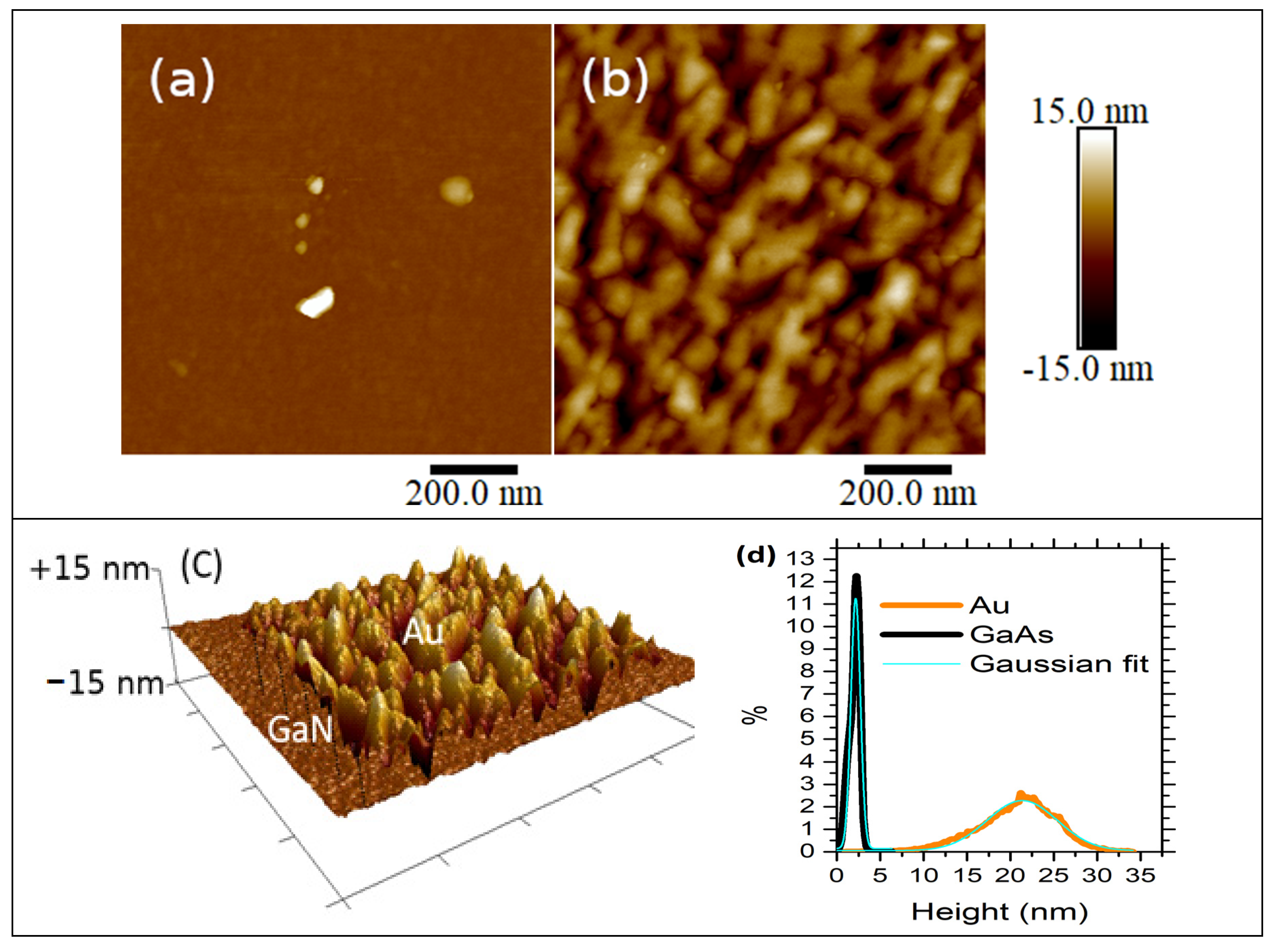
2. The Experiment
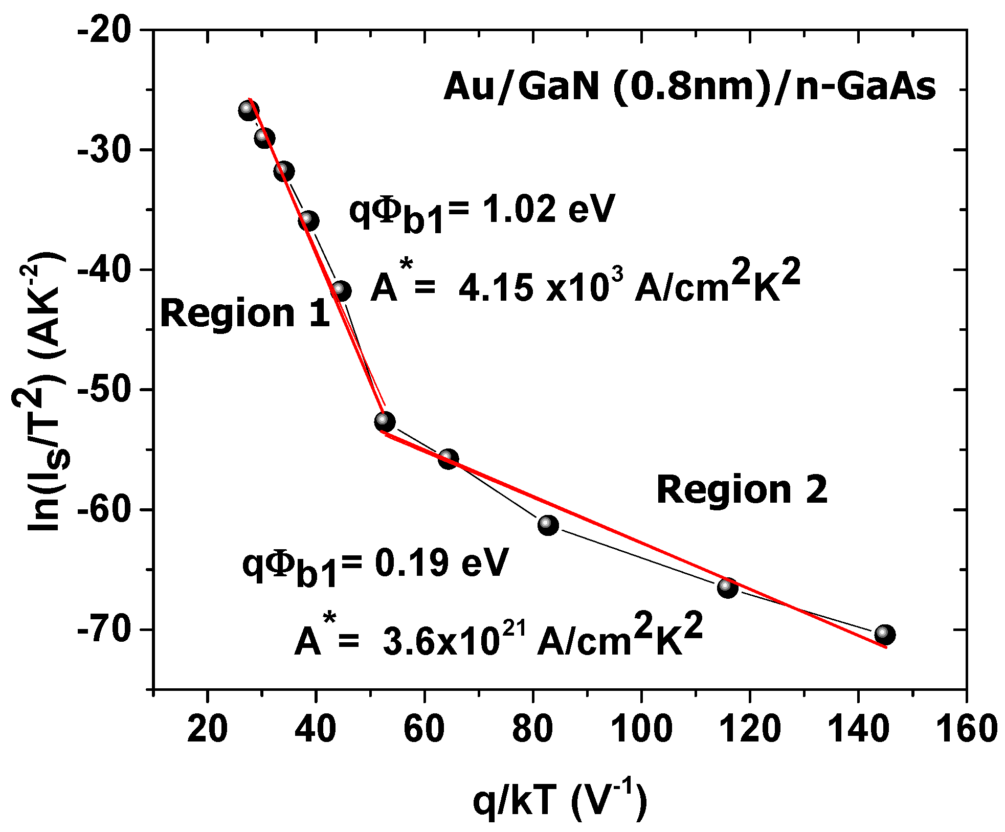
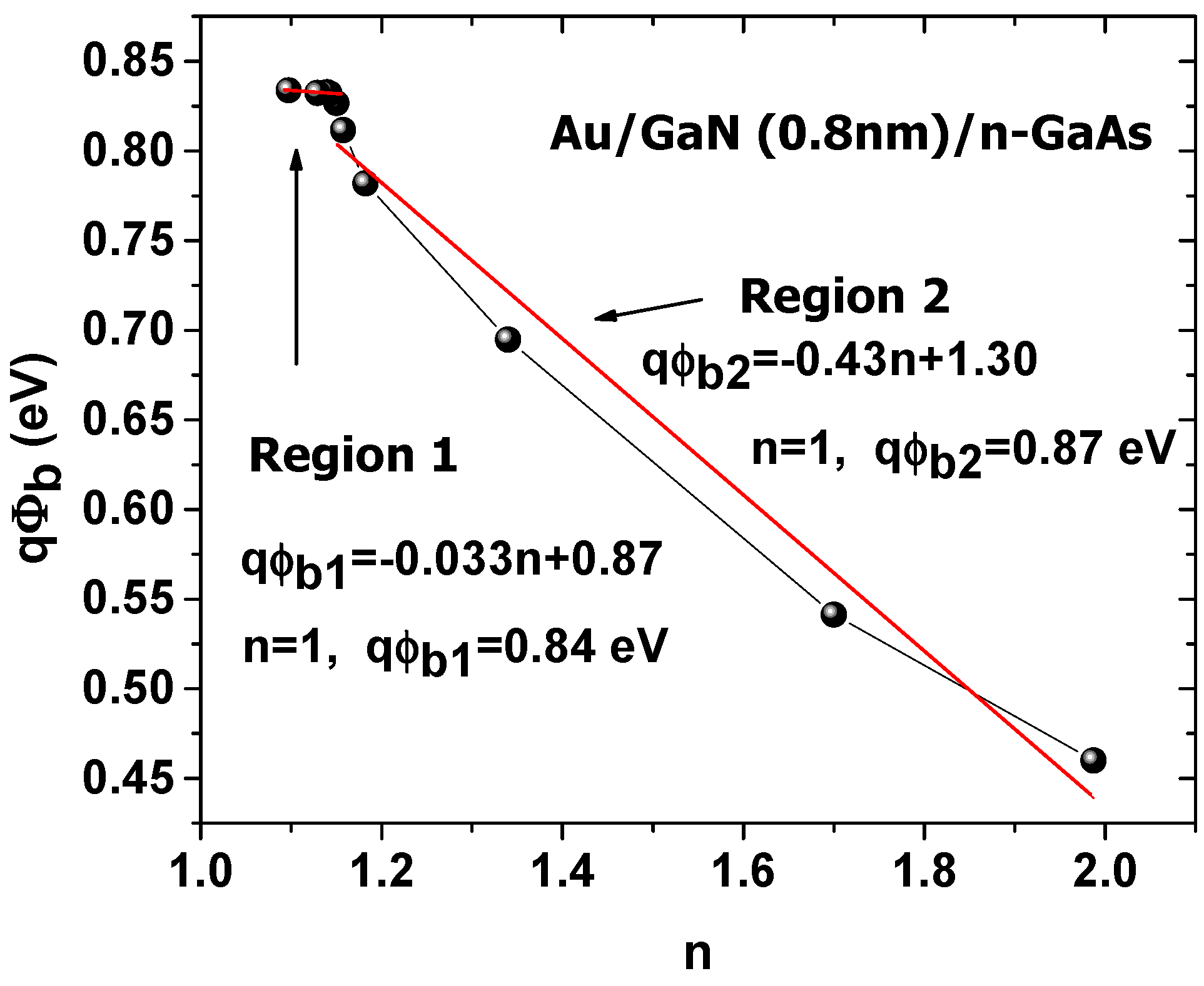
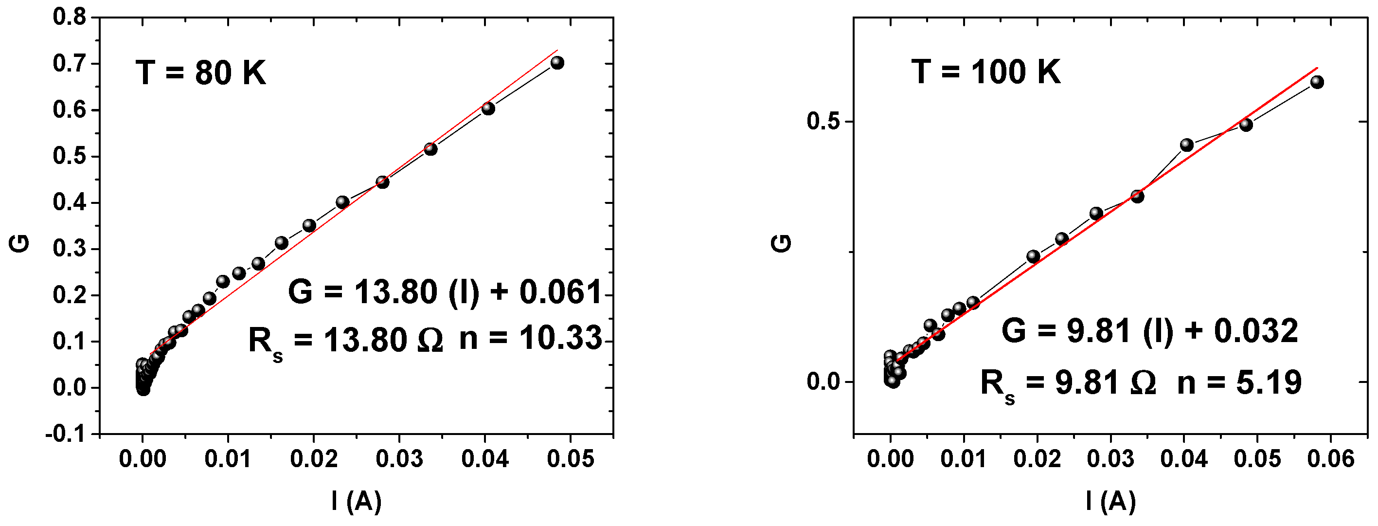
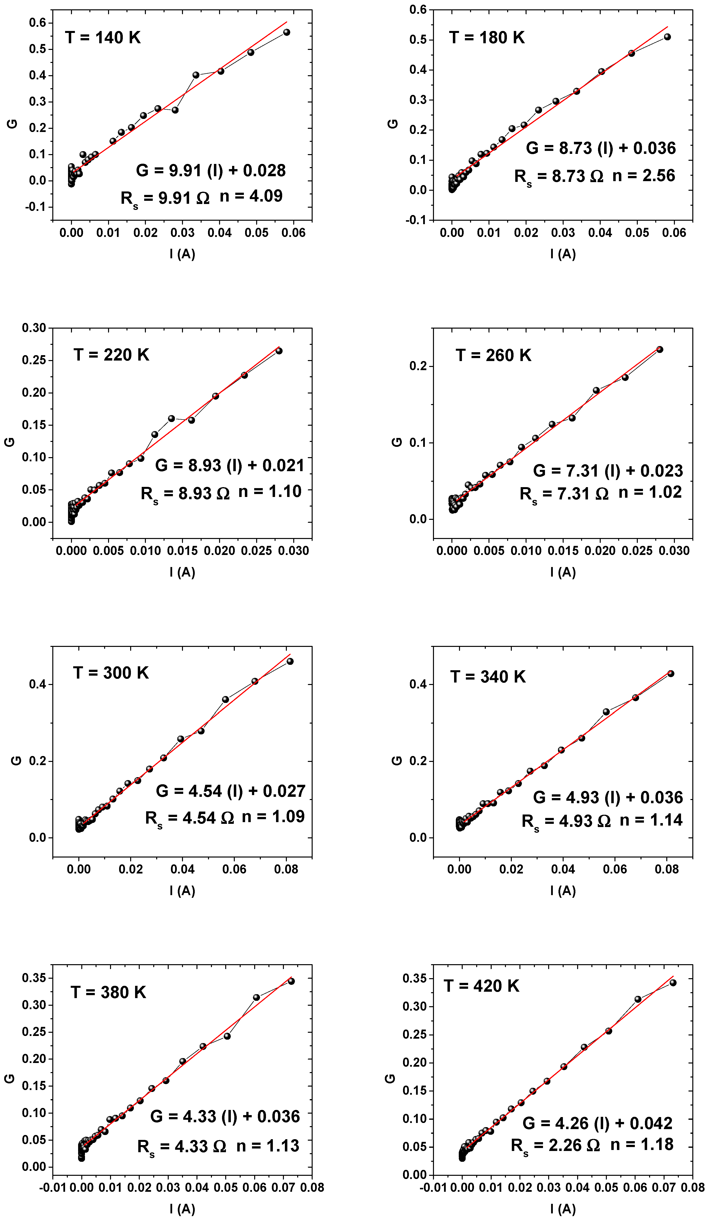
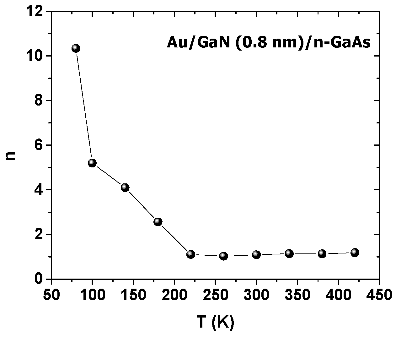
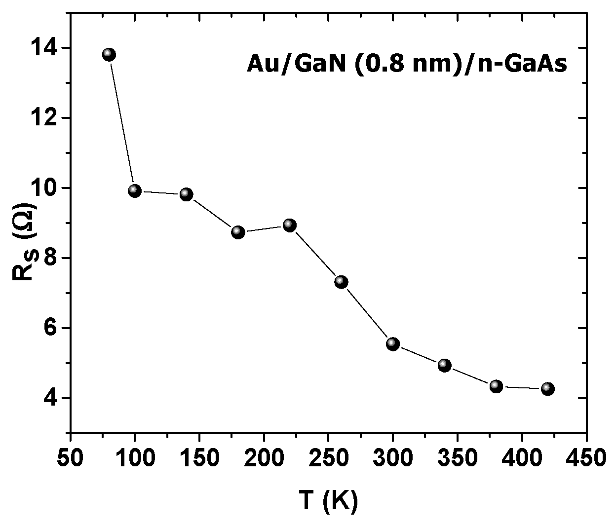
3. The Results
4. Conclusions
Author Contributions
Funding
Institutional Review Board Statement
Informed Consent Statement
Data Availability Statement
Acknowledgments
Conflicts of Interest
References
- Rhoderick, E.; Williams, R. Metal–Semiconductor Contacts; Clarendon Press: Oxford, UK, 1988. [Google Scholar]
- Sze, S.M.; Ng, K.K. Physics of Semiconductor Devices; John Wiley & Sons: Hobocken, NJ, USA, 2006. [Google Scholar]
- Demircioglu, Ö.; Karataş, Ş.; Yıldırım, N.; Bakkaloglu, Ö.; Türüt, A. Temperature dependent current–voltage and capacitance–voltage characteristics of chromium Schottky contacts formed by electrodeposition technique on n-type Si. J. Alloy. Compd. 2011, 509, 6433–6439. [Google Scholar] [CrossRef]
- Korucu, D.; Turut, A.; Altındal, Ş. The origin of negative capacitance in Au/n-GaAs Schottky barrier diodes (SBDs) prepared by photolithography technique in the wide frequency range. Curr. Appl. Phys. 2013, 13, 1101–1108. [Google Scholar] [CrossRef]
- Helal, H.; Benamara, Z.; Arbia, M.B.; Khettou, A.; Rabehi, A.; Kacha, A.H.; Amrani, M. A study of current-voltage and capacitance-voltage characteristics of Au/n-GaAs and Au/GaN/n-GaAs Schottky diodes in wide temperature range. Int. J. Numer. Model. Electron. Netw. Devices Fields 2020, 33, e2714. [Google Scholar] [CrossRef]
- Zeyrek, S.; Bülbül, M.; Altındal, Ş.; Baykul, M.; Yüzer, H. The double gaussian distribution of inhomogeneous barrier heights in Al/GaN/p-GaAs (MIS) schottky diodes in wide temperature range. Braz. J. Phys. 2008, 38, 591–597. [Google Scholar]
- Hardikar, S.; Hudait, M.; Modak, P.; Krupanidhi, S.; Padha, N. Anomalous current transport in Au/low-doped n-GaAs Schottky barrier diodes at low temperatures. Appl. Phys. 1999, 68, 49–55. [Google Scholar] [CrossRef]
- Kumar, A.; Arafin, S.; Amann, M.C.; Singh, R. Temperature dependence of electrical characteristics of Pt/GaN Schottky diode fabricated by UHV e-beam evaporation. Nanoscale Res. Lett. 2013, 8, 481. [Google Scholar] [CrossRef] [Green Version]
- Osvald, J.; Horvath, Z.J. Theoretical study of the temperature dependence of electrical characteristics of Schottky diodes with an inverse near-surface layer. Appl. Surf. Sci. 2004, 234, 349–354. [Google Scholar] [CrossRef]
- Tunhuma, S.M.; Auret, F.D.; Legodi, M.J.; Diale, M. The effect of high temperatures on the electrical characteristics of Au/n-GaAs Schottky diodes. Phys. B Condens. Matter 2016, 480, 201–205. [Google Scholar] [CrossRef] [Green Version]
- Özavcı, E.; Demirezen, S.; Aydemir, U.; Altındal, Ş. A detailed study on current–voltage characteristics of Au/n-GaAs in wide temperature range. Sens. Actuators A Phys. 2013, 194, 259–268. [Google Scholar] [CrossRef]
- Werner, J.H.; Güttler, H.H. Barrier inhomogeneities at Schottky contacts. J. Appl. Phys. 1991, 69, 1522–1533. [Google Scholar] [CrossRef]
- Sullivan, J.; Tung, R.; Pinto, M.; Graham, W. Electron transport of inhomogeneous Schottky barriers: A numerical study. J. Appl. Phys. 1991, 70, 7403–7424. [Google Scholar] [CrossRef]
- Tung, R. Electron transport at metal-semiconductor interfaces: General theory. Phys. Rev. 1992, 45, 13509. [Google Scholar] [CrossRef]
- Schmitsdorf, R.; Kampen, T.; Mönch, W. Explanation of the linear correlation between barrier heights and ideality factors of real metal-semiconductor contacts by laterally nonuniform Schottky barriers. J. Vac. Sci. Technol. B Microelectron. Nanometer Struct. Process. Meas. Phenom. 1997, 15, 1221–1226. [Google Scholar] [CrossRef]
- Palm, H.; Arbes, M.; Schulz, M. Fluctuations of the Au-Si (100) Schottky barrier height. Phys. Rev. Lett. 1993, 71, 2224. [Google Scholar] [CrossRef]
- Vanalme, G.; Goubert, L.; van Meirhaeghe, R.; Cardon, F.; van Daele, P. A ballistic electron emission microscopy study of barrier height inhomogeneities introduced in Au/III-V semiconductor Schottky barrier contacts by chemical pretreatments. Semicond. Sci. Technol. 1999, 14, 871. [Google Scholar] [CrossRef]
- Chin, V.W.; Green, M.; Storey, J.W. Evidence for multiple barrier heights in P-type PtSi Schottky-barrier diodes from IVT and photoresponse measurements. Solid-State Electron. 1990, 33, 299–308. [Google Scholar] [CrossRef]
- Singh, A.; Reinhardt, K.; Anderson, W. Temperature dependence of the electrical characteristics of Yb/p-InP tunnel metal-insulator-semiconductor junctions. J. Appl. Phys. 1990, 68, 3475–3483. [Google Scholar] [CrossRef]
- Chand, S.; Kumar, J. Current transport in Pd 2 Si/n-Si (100) Schottky barrier diodes at low temperatures. Appl. Phys. 1996, 63, 171–178. [Google Scholar] [CrossRef]
- McCafferty, P.; Sellai, A.; Dawson, P.; Elabd, H. Barrier characteristics of PtSip-Si Schottky diodes as determined from IVT measurements. Solid-State Electron. 1996, 39, 583–592. [Google Scholar] [CrossRef]
- Zhu, S.; van Meirhaeghe, R.; Detavernier, C.; Ru, G.-P.; Li, B.-Z.; Cardon, F. A BEEM study of the temperature dependence of the barrier height distribution in PtSi/n-Si Schottky diodes. Solid state Commun. 1999, 112, 611–615. [Google Scholar] [CrossRef]
- Zhu, S.; van Meirhaeghe, R.; Detavernier, C.; Cardon, F.; Ru, G.-P.; Qu, X.-P.; Li, B.-Z. Barrier height inhomogeneities of epitaxial CoSi2 Schottky contacts on n-Si (100) and (111). Solid-State Electron. 2000, 44, 663–671. [Google Scholar] [CrossRef]
- Korucu, D.; Turut, A.; Efeoglu, H. Temperature dependent I–V characteristics of an Au/n-GaAs Schottky diode analyzed using Tung’s model. Phys. B Condens. Matter 2013, 414, 35–41. [Google Scholar] [CrossRef]
- Crowell, C. The physical significance of the T0 anomalies in Schottky barriers. Solid-State Electron. 1977, 20, 171–175. [Google Scholar] [CrossRef]
- Hudait, M.; Venkateswarlu, P.; Krupanidhi, S. Electrical transport characteristics of Au/n-GaAs Schottky diodes on n-Ge at low temperatures. Solid-State Electron. 2001, 45, 133–141. [Google Scholar] [CrossRef] [Green Version]
- Helal, H.; Benamara, Z.; Kacha, A.H.; Amrani, M.; Rabehi, A.; Akkal, B.; Monier, G.; Robert-Goumet, C. Comparative study of ionic bombardment and heat treatment on the electrical behavior of Au/GaN/n-GaAs Schottky diodes. Superlattices Microstruct. 2019, 135, 106276. [Google Scholar] [CrossRef]
- Uslu, H.; Bengi, A.; Çetin, S.; Aydemir, U.; Altındal, Ş.; Aghaliyeva, S.; Özçelik, S. Temperature and voltage dependent current-transport mechanisms in GaAs/AlGaAs single-quantum-well lasers. J. Alloy. Compd. 2010, 507, 190–195. [Google Scholar] [CrossRef]
- Dawidowski, W.; Ściana, B.; Bielak, K.; Mikolášek, M.; Drobný, J.; Serafińczuk, J.; Lombardero, I.; Radziewicz, D.; Kijaszek, W.; Kósa, A. Analysis of Current Transport Mechanism in AP-MOVPE Grown GaAsN pin Solar Cell. Energies 2021, 14, 4651. [Google Scholar] [CrossRef]
- Rabehi, A.; Amrani, M.; Benamara, Z.; Akkal, B.; Hatem-Kacha, A.; Robert-Goumet, C.; Monier, G.; Gruzza, B. Study of the characteristics current-voltage and capacitance-voltage in nitride GaAs Schottky diode. Eur. Phys. J. Appl. Phys. 2015, 72, 10102. [Google Scholar] [CrossRef]
- Güllü, Ö.; Biber, M.; Duman, S.; Türüt, A. Electrical characteristics of the hydrogen pre-annealed Au/n-GaAs Schottky barrier diodes as a function of temperature. Appl. Surf. Sci. 2007, 253, 7246–7253. [Google Scholar] [CrossRef]
- Ayyildiz, E.; Cetin, H.; Horvath, Z.J. Temperature dependent electrical characteristics of Sn/p-Si Schottky diodes. Appl. Surf. Sci. 2005, 252, 1153–1158. [Google Scholar] [CrossRef]
- Horvath, Z.J.; Rakovics, V.; Szentpali, B.; Püspöki, S.; Žd’ánský, K. InP Schottky junctions for zero bias detector diodes. Vacuum 2003, 71, 113–116. [Google Scholar] [CrossRef]
- Altındal, Ş.; Karadeniz, S.; Tuğluoğlu, N.; Tataroğlu, A. The role of interface states and series resistance on the I–V and C–V characteristics in Al/SnO2/p-Si Schottky diodes. Solid-State Electron. 2003, 47, 1847–1854. [Google Scholar] [CrossRef]
- Matolın, V.; Fabık, S.; Glosık, J.; Bideux, L.; Ould-Metidji, Y.; Gruzza, B. Experimental system for GaN thin films growth and in situ characterisation by electron spectroscopic methods. Vacuum 2004, 76, 471–476. [Google Scholar] [CrossRef]
- Ould-Metidji, Y.; Bideux, L.; Baca, D.; Gruzza, B.; Matolin, V. Nitridation of GaAs (1 0 0) substrates and Ga/GaAs systems studied by XPS spectroscopy. Appl. Surf. Sci. 2003, 212, 614–618. [Google Scholar] [CrossRef]
- Benamara, Z.; Mecirdi, N.; Bouiadjra, B.B.; Bideux, L.; Gruzza, B.; Robert, C.; Miczek, M.; Adamowicz, B. XPS, electric and photoluminescence-based analysis of the GaAs (1 0 0) nitridation. Appl. Surf. Sci. 2006, 252, 7890–7894. [Google Scholar] [CrossRef]
- Kacha, A.; Akkal, B.; Benamara, Z.; Amrani, M.; Rabhi, A.; Monier, G.; Robert-Goumet, C.; Bideux, L.; Gruzza, B. Effects of the GaN layers and the annealing on the electrical properties in the Schottky diodes based on nitrated GaAs. Superlattices Microstruct. 2015, 83, 827–833. [Google Scholar] [CrossRef]
- Mehdi, H.; Monier, G.; Hoggan, P.; Bideux, L.; Robert-Goumet, C.; Dubrovskii, V. Combined angle-resolved X-ray photoelectron spectroscopy, density functional theory and kinetic study of nitridation of gallium arsenide. Appl. Surf. Sci. 2018, 427, 662–669. [Google Scholar] [CrossRef]
- Rabehi, A.; Amrani, M.; Benamara, Z.; Akkal, B.; Kacha, A. Electrical and photoelectrical characteristics of Au/GaN/GaAs Schottky diode. Optik 2016, 127, 6412–6418. [Google Scholar] [CrossRef]
- Ambrico, M.; Losurdo, M.; Capezzuto, P.; Bruno, G.; Ligonzo, T.; Haick, H. Probing electrical properties of molecule-controlled or plasma-nitrided GaAs surfaces: Two different tools for modifying the electrical characteristics of metal/GaAs diodes. Appl. Surf. Sci. 2006, 252, 7636–7641. [Google Scholar] [CrossRef]
- Bideux, L.; Monier, G.; Matolin, V.; Robert-Goumet, C.; Gruzza, B. XPS study of the formation of ultrathin GaN film on GaAs (1 0 0). Appl. Surf. Sci. 2008, 254, 4150–4153. [Google Scholar] [CrossRef]
- Kacha, A.; Akkal, B.; Benamara, Z.; Robert-Goumet, C.; Monier, G.; Gruzza, B. Study of the surface state density and potential in MIS diode Schottky using the surface photovoltage method. Mol. Cryst. Liq. Cryst. 2016, 627, 66–73. [Google Scholar] [CrossRef]
- Berkovits, V.; L’vova, T.; Ulin, V. Chemical nitridation of GaAs (100) by hydrazine-sulfide water solutions. Vacuum 2000, 57, 201–207. [Google Scholar] [CrossRef]
- Monier, G.; Bideux, L.; Robert-Goumet, C.; Gruzza, B.; Petit, M.; Lábár, J.; Menyhárd, M. Passivation of GaAs (001) surface by the growth of high quality c-GaN ultra-thin film using low power glow discharge nitrogen plasma source. Surf. Sci. 2012, 606, 1093–1099. [Google Scholar] [CrossRef]
- Mehdi, H.; Réveret, F.; Bougerol, C.; Robert-Goumet, C.; Hoggan, P.; Bideux, L.; Gruzza, B.; Leymarie, J.; Monier, G. Study of GaN layer crystallization on GaAs (100) using electron cyclotron resonance or glow discharge N2 plasma sources for the nitriding process. Appl. Surf. Sci. 2019, 495, 143586. [Google Scholar] [CrossRef]
- Ozdemir, M.; Sevgili, O.; Orak, I.; Turut, A. Determining the potential barrier presented by the interfacial layer from the temperature induced IV characteristics in Al/p-Si Structure with native oxide layer. Mater. Sci. Semicond. Process. 2021, 125, 105629. [Google Scholar] [CrossRef]
- Cheung, S.; Cheung, N. Extraction of Schottky diode parameters from forward current-voltage characteristics. Appl. Phys. Lett. 1986, 49, 85–87. [Google Scholar] [CrossRef]
- Horváth, Z.J. A New Approach to Temperature Dependent Ideality Factors in Schottky Contacts. MRS Online Proc. Libr. Arch. 1992, 260, 359–366. [Google Scholar] [CrossRef]
- Hackam, R.; Harrop, P. Electrical properties of nickel-low-doped n-type gallium arsenide Schottky-barrier diodes. IEEE Trans. Electron. Devices 1972, 19, 1231–1238. [Google Scholar] [CrossRef]
- Bhuiyan, A.; Martinez, A.; Esteve, D. A new Richardson plot for non-ideal schottky diodes. Thin Solid Film. 1988, 161, 93–100. [Google Scholar] [CrossRef]
- Bengi, A.; Altındal, S.; Özçelik, S.; Mammadov, T. Gaussian distribution of inhomogeneous barrier height in Al0. 24Ga0. 76As/GaAs structures. Phys. B Condens. Matter 2007, 396, 22–28. [Google Scholar] [CrossRef]
- Werner, J.H. Schottky barrier and pn-junctionI/V plots—Small signal evaluation. Appl. Phys. 1988, 47, 291–300. [Google Scholar] [CrossRef]
- Panish, M.; Casey, H.C., Jr. Temperature dependence of the energy gap in GaAs and GaP. J. Appl. Phys. 1969, 40, 163–167. [Google Scholar] [CrossRef]
- Padovani, F.; Sumner, G. Experimental Study of Gold-Gallium Arsenide Schottky Barriers. J. Appl. Phys. 1965, 36, 3744–3747. [Google Scholar] [CrossRef]
- Padovani, F. Graphical determination of the barrier height and excess temperature of a Schottky barrier. J. Appl. Phys. 1966, 37, 921–922. [Google Scholar] [CrossRef]
- Ebeoğlu, M.A. Current–voltage characteristics of Au/GaN/GaAs structure. Phys. B Condens. Matter 2008, 403, 61–66. [Google Scholar] [CrossRef]
- Schmitsdorf, R.; Kampen, T.; Mönch, W. Correlation between barrier height and interface structure of AgSi (111) Schottky diodes. Surf. Sci. 1995, 324, 249–256. [Google Scholar] [CrossRef]
- Soylu, M.; Yakuphanoglu, F. Analysis of barrier height inhomogeneity in Au/n-GaAs Schottky barrier diodes by Tung model. J. Alloy. Compd. 2010, 506, 418–422. [Google Scholar] [CrossRef]


Publisher’s Note: MDPI stays neutral with regard to jurisdictional claims in published maps and institutional affiliations. |
© 2021 by the authors. Licensee MDPI, Basel, Switzerland. This article is an open access article distributed under the terms and conditions of the Creative Commons Attribution (CC BY) license (https://creativecommons.org/licenses/by/4.0/).
Share and Cite
Helal, H.; Benamara, Z.; Wederni, M.A.; Mourad, S.; Khirouni, K.; Monier, G.; Robert-Goumet, C.; Rabehi, A.; Hatem Kacha, A.; Bakkali, H.; et al. Conduction Mechanisms in Au/0.8 nm–GaN/n–GaAs Schottky Contacts in a Wide Temperature Range. Materials 2021, 14, 5909. https://doi.org/10.3390/ma14205909
Helal H, Benamara Z, Wederni MA, Mourad S, Khirouni K, Monier G, Robert-Goumet C, Rabehi A, Hatem Kacha A, Bakkali H, et al. Conduction Mechanisms in Au/0.8 nm–GaN/n–GaAs Schottky Contacts in a Wide Temperature Range. Materials. 2021; 14(20):5909. https://doi.org/10.3390/ma14205909
Chicago/Turabian StyleHelal, Hicham, Zineb Benamara, Mouhamed Amine Wederni, Sabrine Mourad, Kamel Khirouni, Guillaume Monier, Christine Robert-Goumet, Abdelaziz Rabehi, Arslane Hatem Kacha, Hicham Bakkali, and et al. 2021. "Conduction Mechanisms in Au/0.8 nm–GaN/n–GaAs Schottky Contacts in a Wide Temperature Range" Materials 14, no. 20: 5909. https://doi.org/10.3390/ma14205909
APA StyleHelal, H., Benamara, Z., Wederni, M. A., Mourad, S., Khirouni, K., Monier, G., Robert-Goumet, C., Rabehi, A., Hatem Kacha, A., Bakkali, H., Gontard, L. C., & Dominguez, M. (2021). Conduction Mechanisms in Au/0.8 nm–GaN/n–GaAs Schottky Contacts in a Wide Temperature Range. Materials, 14(20), 5909. https://doi.org/10.3390/ma14205909