Magnetic Material Assessment of a Novel Ultra-High Step-Up Converter with Single Semiconductor Switch and Galvanic Isolation for Fuel-Cell Power System

Abstract
:1. Introduction
- (1)
- Only one active switch is utilized.
- (2)
- The energy stored in leakage inductance can be recycled.
- (3)
- The voltage conversion ratio is high enough so that SIUSC is capable of dealing with low voltage input.
- (4)
- The structure of the SIUSC has galvanic isolation.
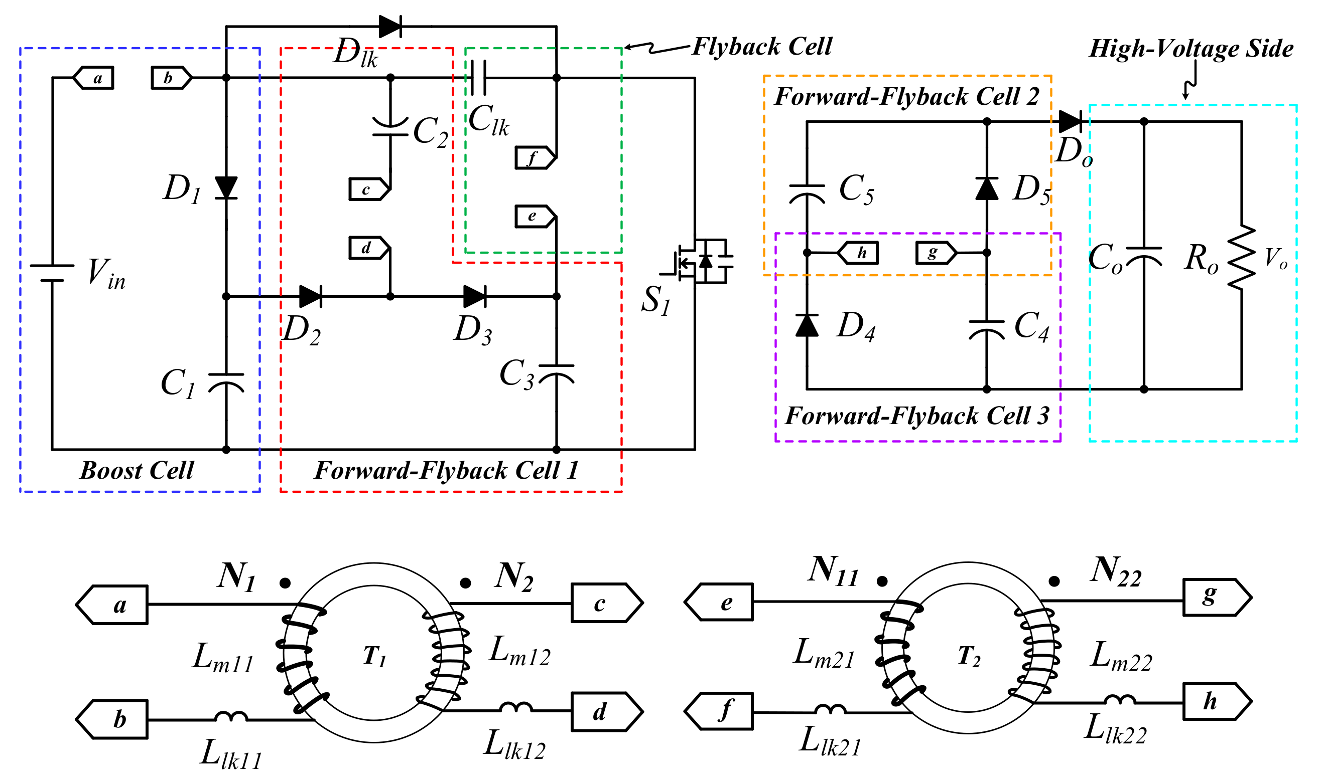
2. Operation Mode of the Proposed Converter
- (1)
- In Figure 1, all of the coupled inductors are in CCM.
- (2)
- Parasitic input capacitance of the main switch, Ciss, is neglected, and all of the diodes are considered ideal.
- (3)
- The capacitances of all capacitors are considered large enough to ignore the ripples across them. Thus, their voltage can be regarded as constant during one switching period.
- (4)
- The turn ratios of T1 and T2 are both equal to n. That is, n1 = n2 = N2/N1 = N22/N11.
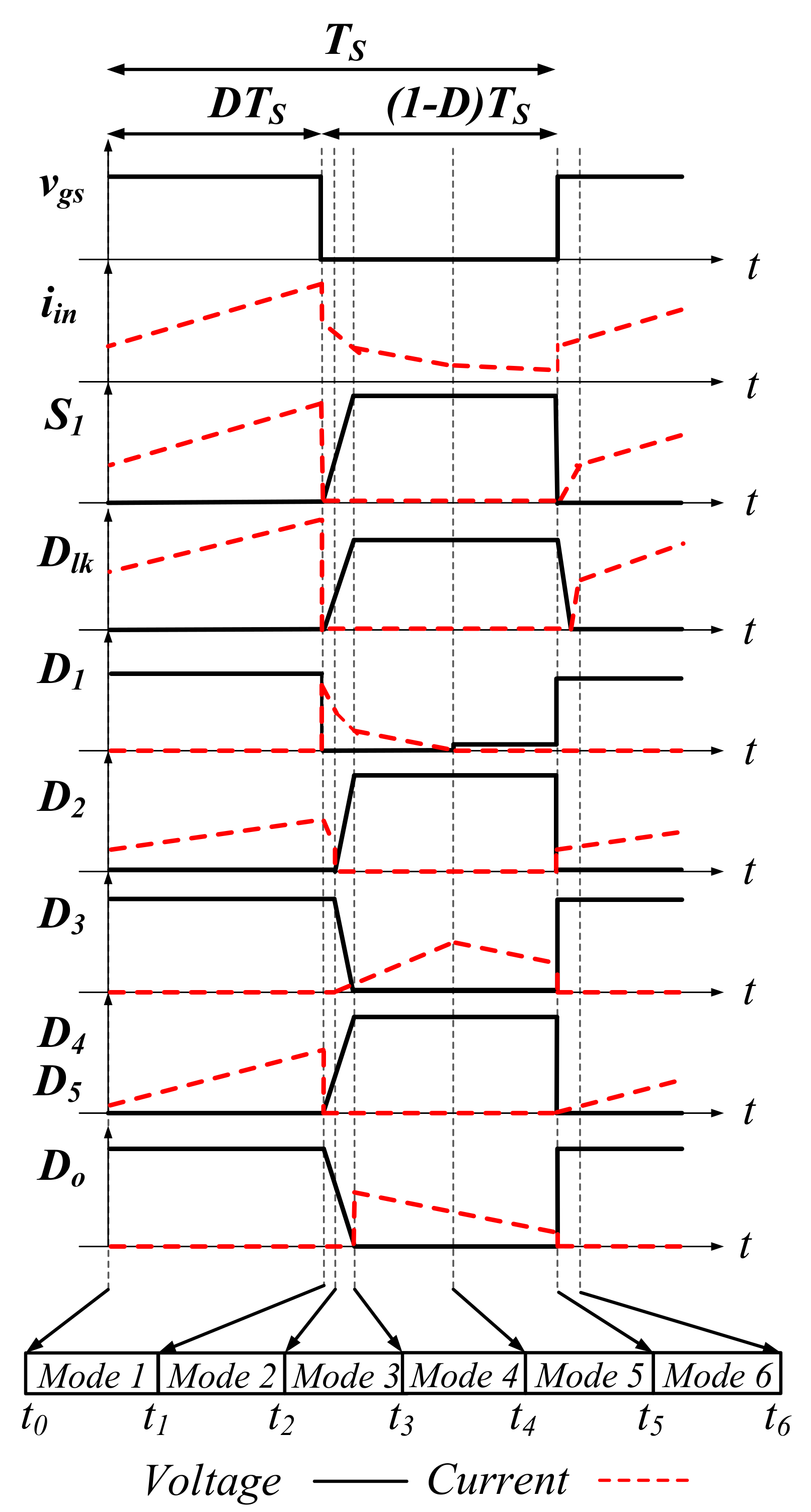
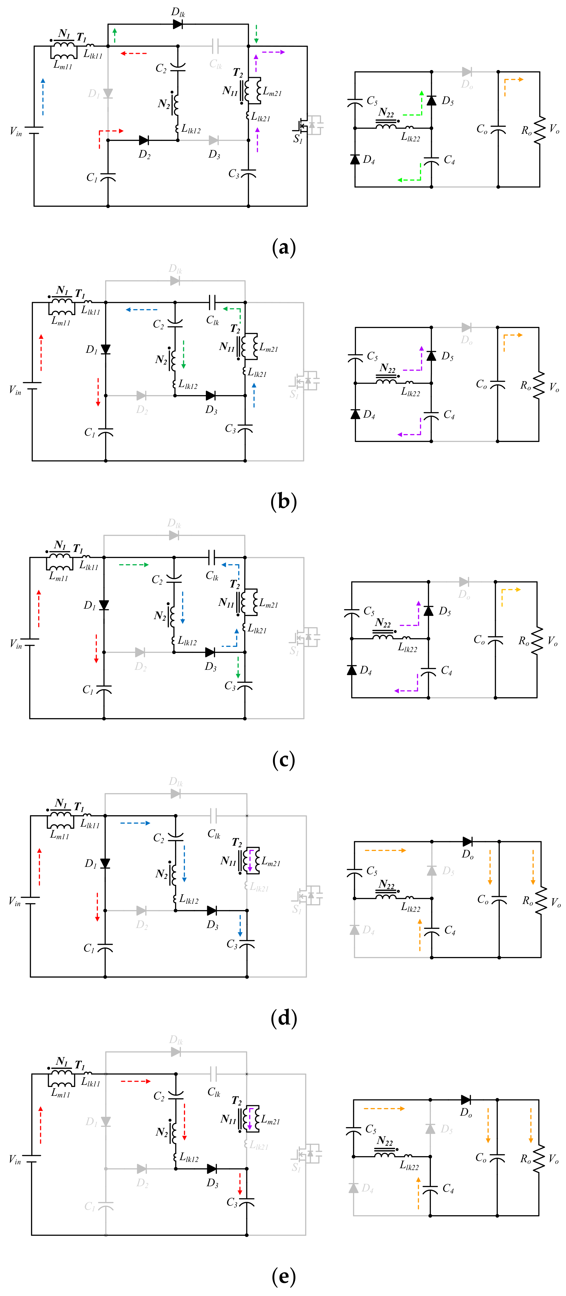
- Mode 1 [t0, t1] (see Figure 2a): The converter operation over one switch cycle starts at Mode 1, in which the switch S1 is turned ON at t = t0. The magnetizing inductors Lm11 and Lm21 absorb energy from Vin and C4, respectively. Meanwhile, capacitor C1 and the secondary of T1 release energy to capacitor C2 via D2 and S1. Once the switch S1 is turned OFF, operation of the converter enters into the next mode.
- Mode 2 [t1, t2] (see Figure 2b): In Mode 2, switch S1 is in OFF state. During this time interval, the energy of Llk11 is forwarded to capacitor C1 via diode D1. Similarly, the energy of Llk21 is dumped to Clk via D3. When iD2 drops to zero, this mode ends.
- Mode 3 [t2, t3] (see Figure 2c): The S1 remains the same status as in Mode 2. The energy of Lm11 is forwarded to capacitor C1. Meanwhile, the capacitor C3 is charged via the loop of Vin-N1-C2-N2-D3. When the capacitor Clk stops absorbing energy from Llk21, this mode ends.
- Mode 4 [t3, t4] (see Figure 2d): During the interval of Mode 4, switch S1 is in OFF state. Input voltage Vin and magnetizing inductance Lm11 proceed with energy releasing toward C1 and C3 via D1 and D3, respectively. In addition, the Lm21 begins pumping its energy to output capacitor Co via the loop of C4-N22-C5-Do-Co. Since C4 and C5 are in series at this energy-pumping loop, both capacitors also forward their energy to Co. The current following through D1, iD1, decreases. Mode 4 ends when iD1 is equal to zero.
- Mode 5 [t4, t5] (see Figure 2e): The switch has the same status as in Mode 4. Since the capacitor C1 has been fully charged, the Lm11 and Lm21 pump energy to C3 and output, respectively. This mode will end as current iDo falls to zero.
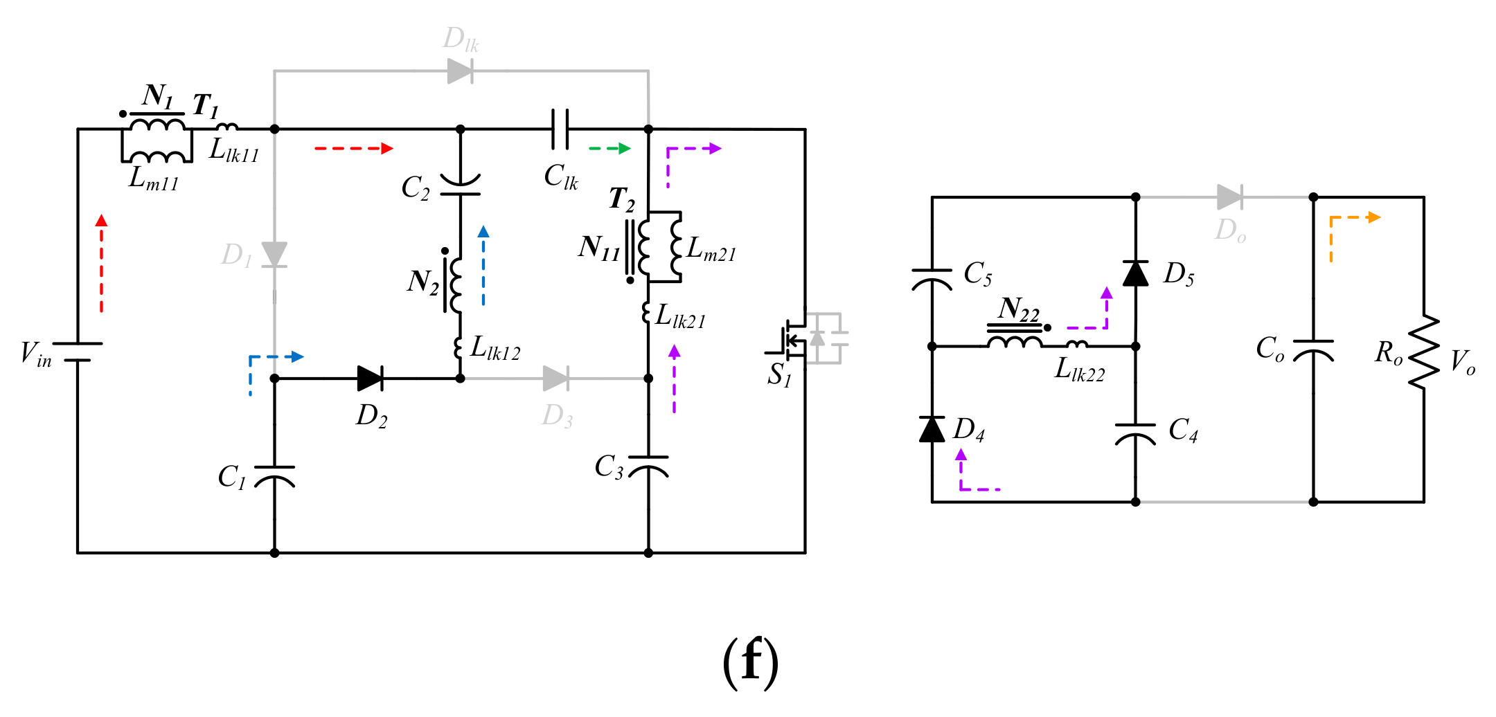
- Mode 6 [t5, t6] (see Figure 2f): In this mode, switch S1 is in ON-state again. The energy stored in capacitor Clk is drawn out via S1; that is, the leakage energy of Llk21 is successfully recycled. This mode ends when iDlk starts to increase, and converter operation over one switching cycle is completed.
3. Voltage Gain Derivation
4. Inductance Design for CCM
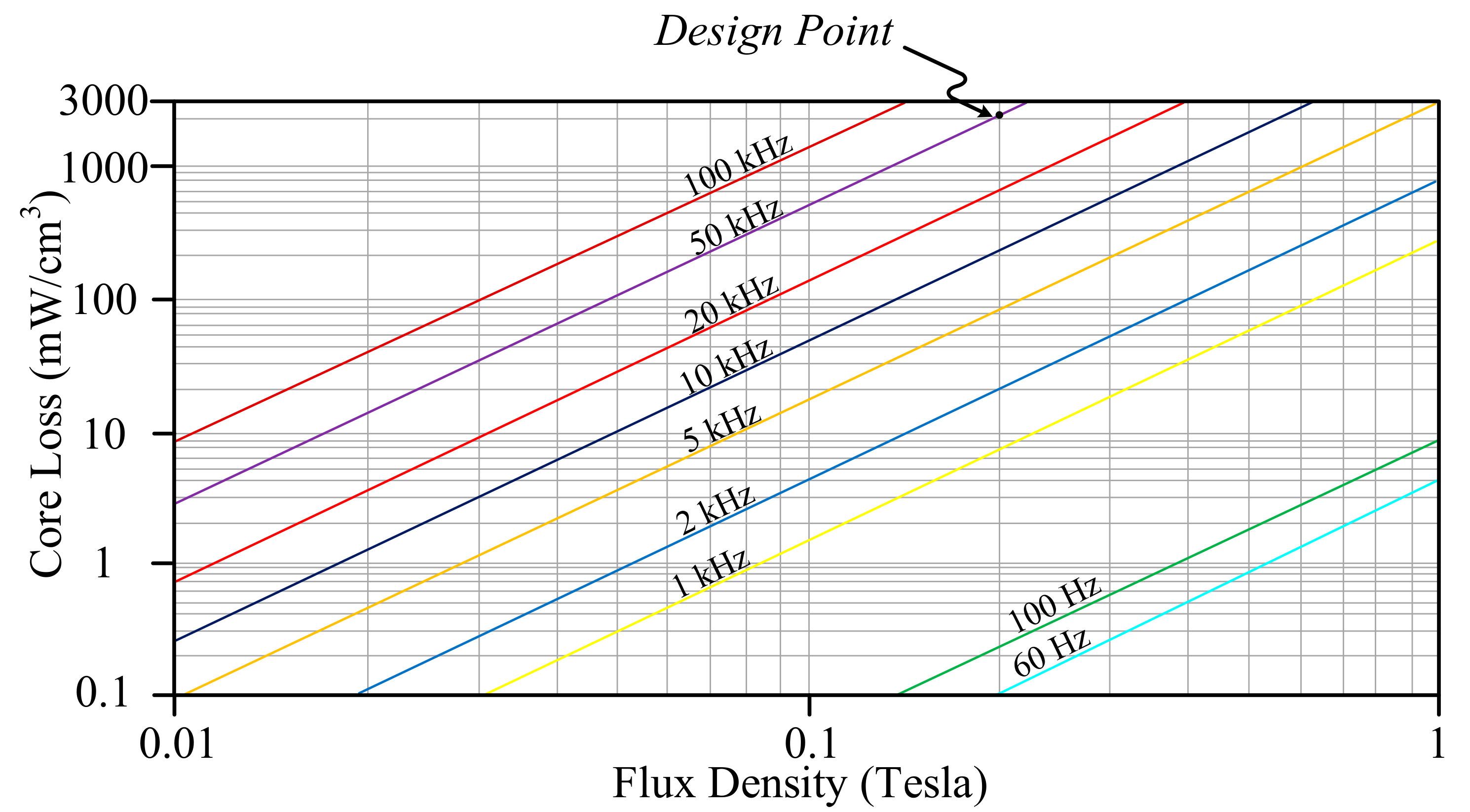
5. Magnetic Core Selection
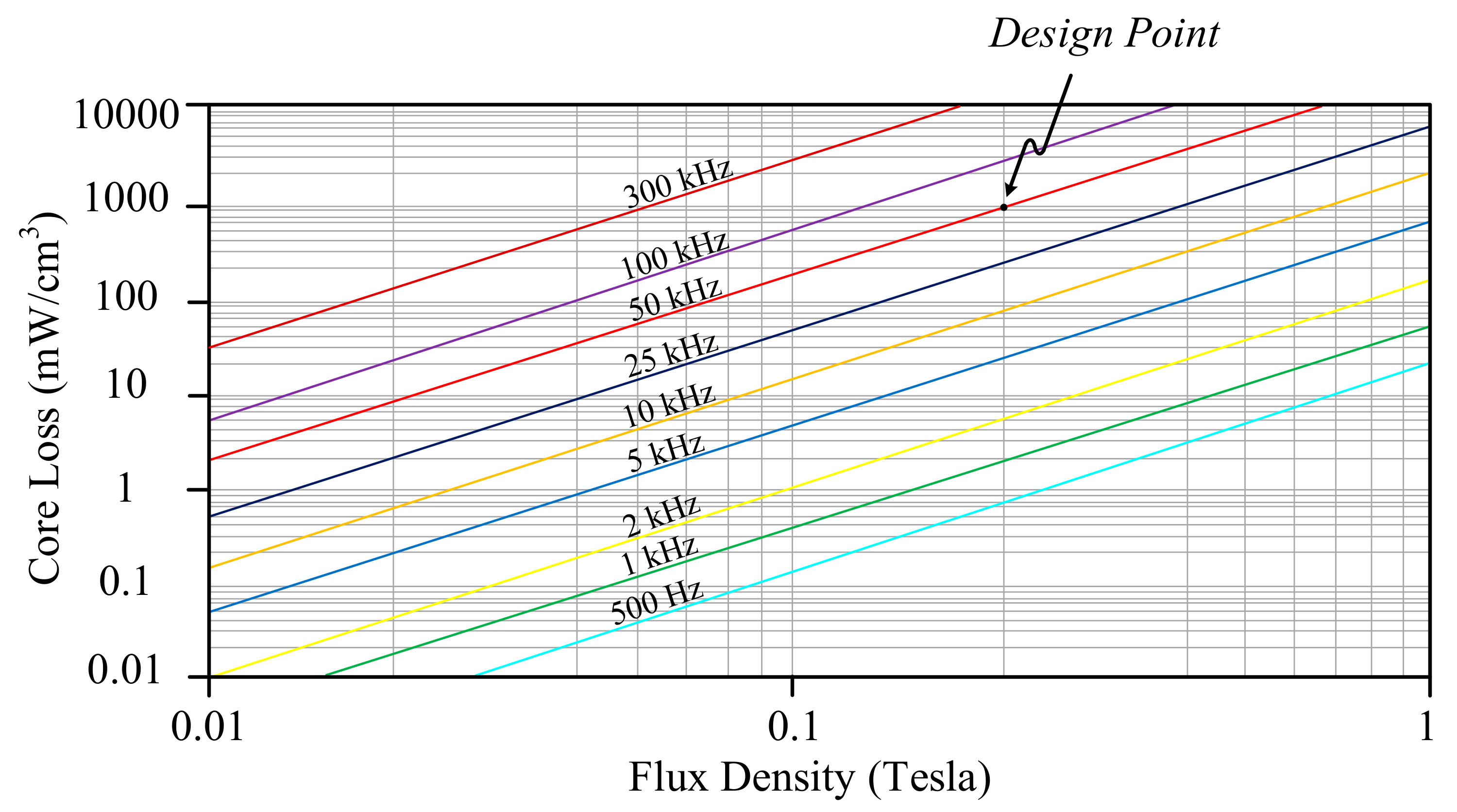
5.1. MPP Core
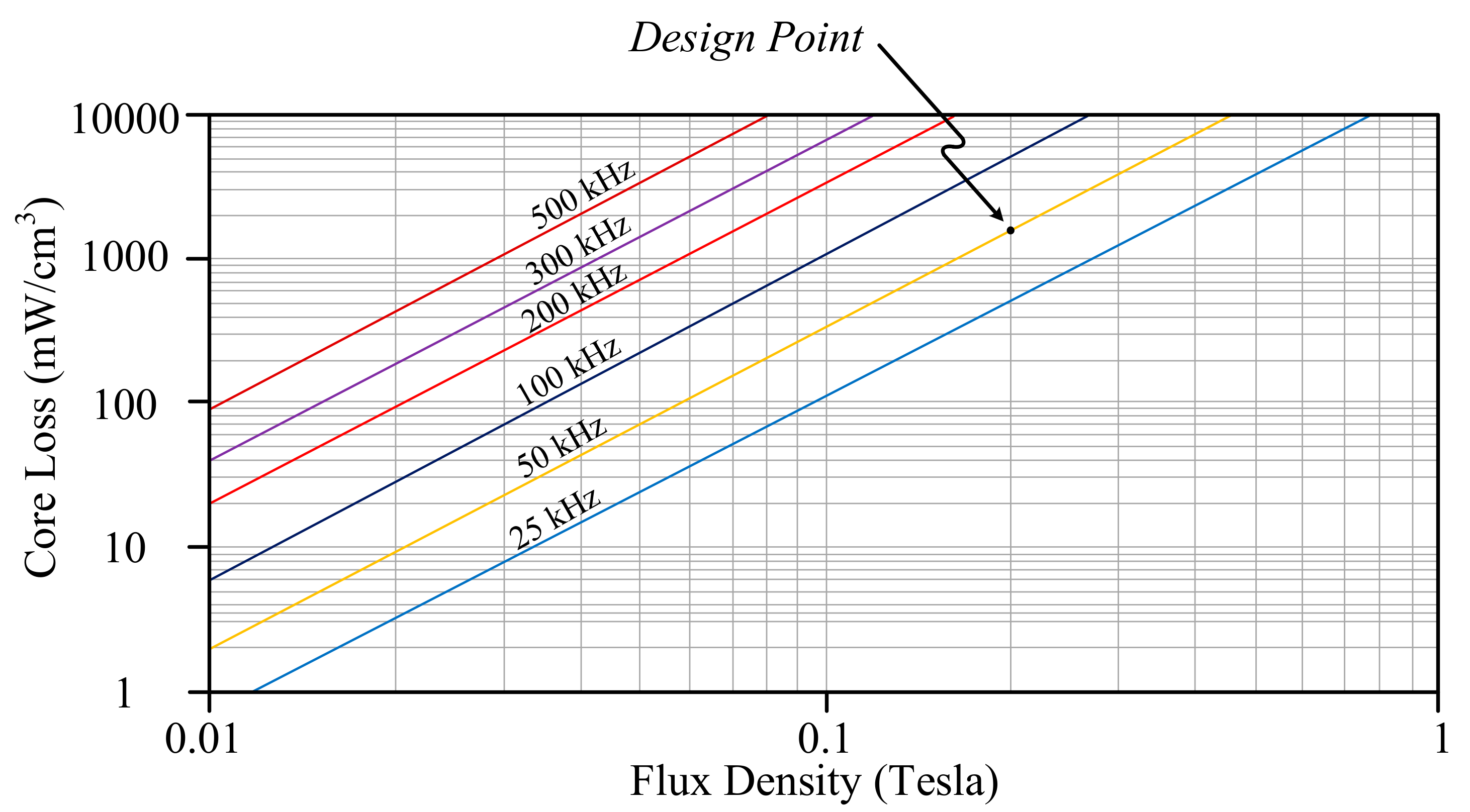
5.2. High Flux Core
5.3. Kool Mμ Core
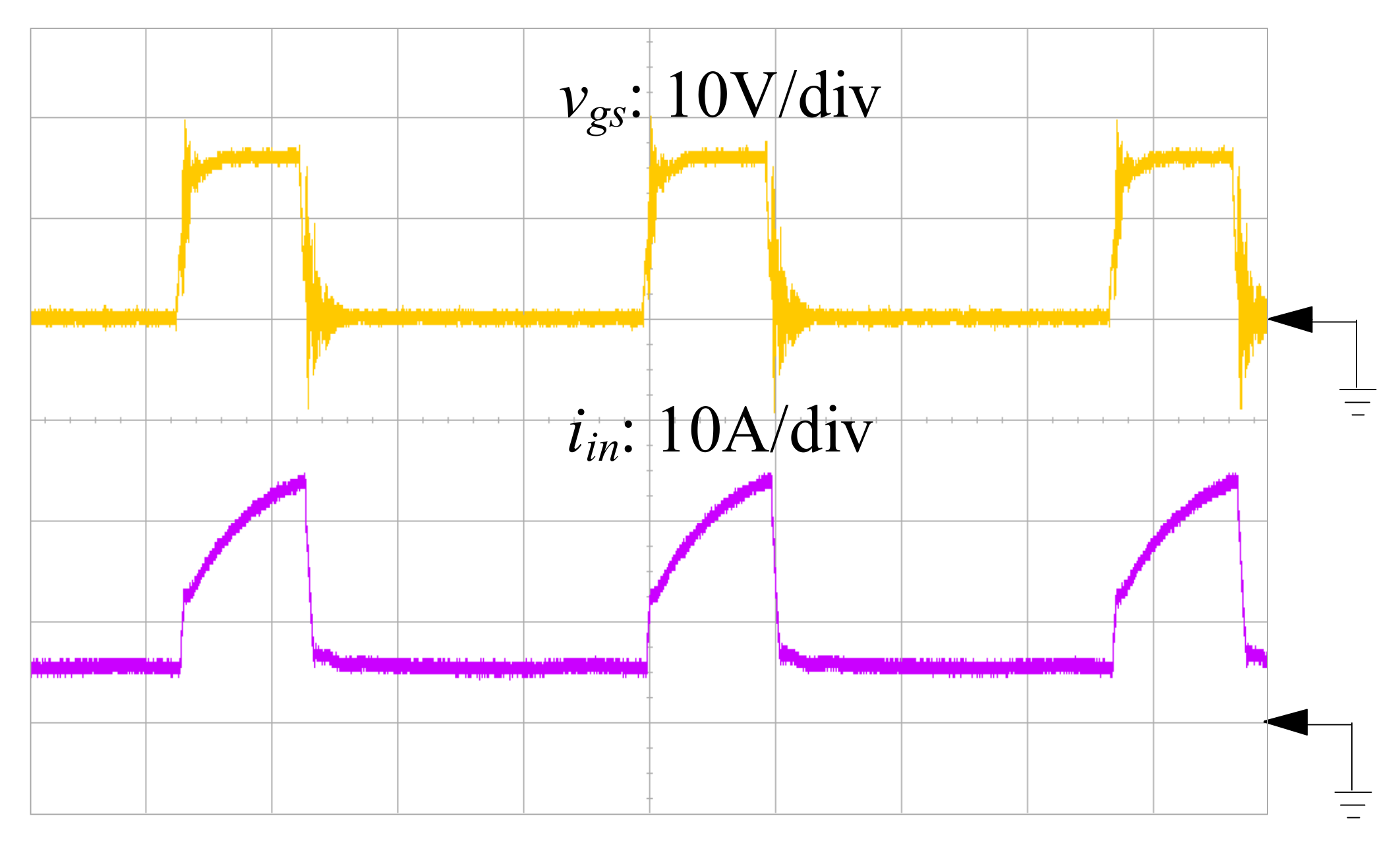
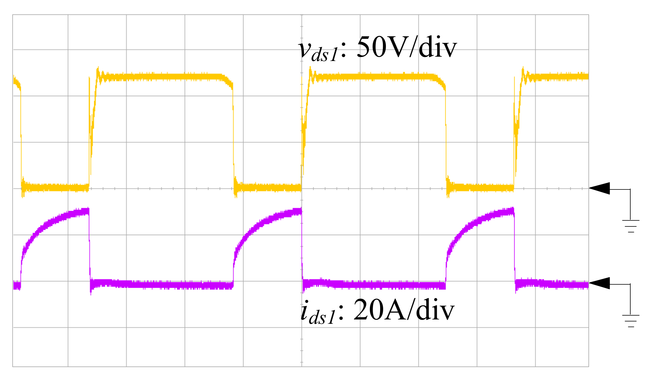
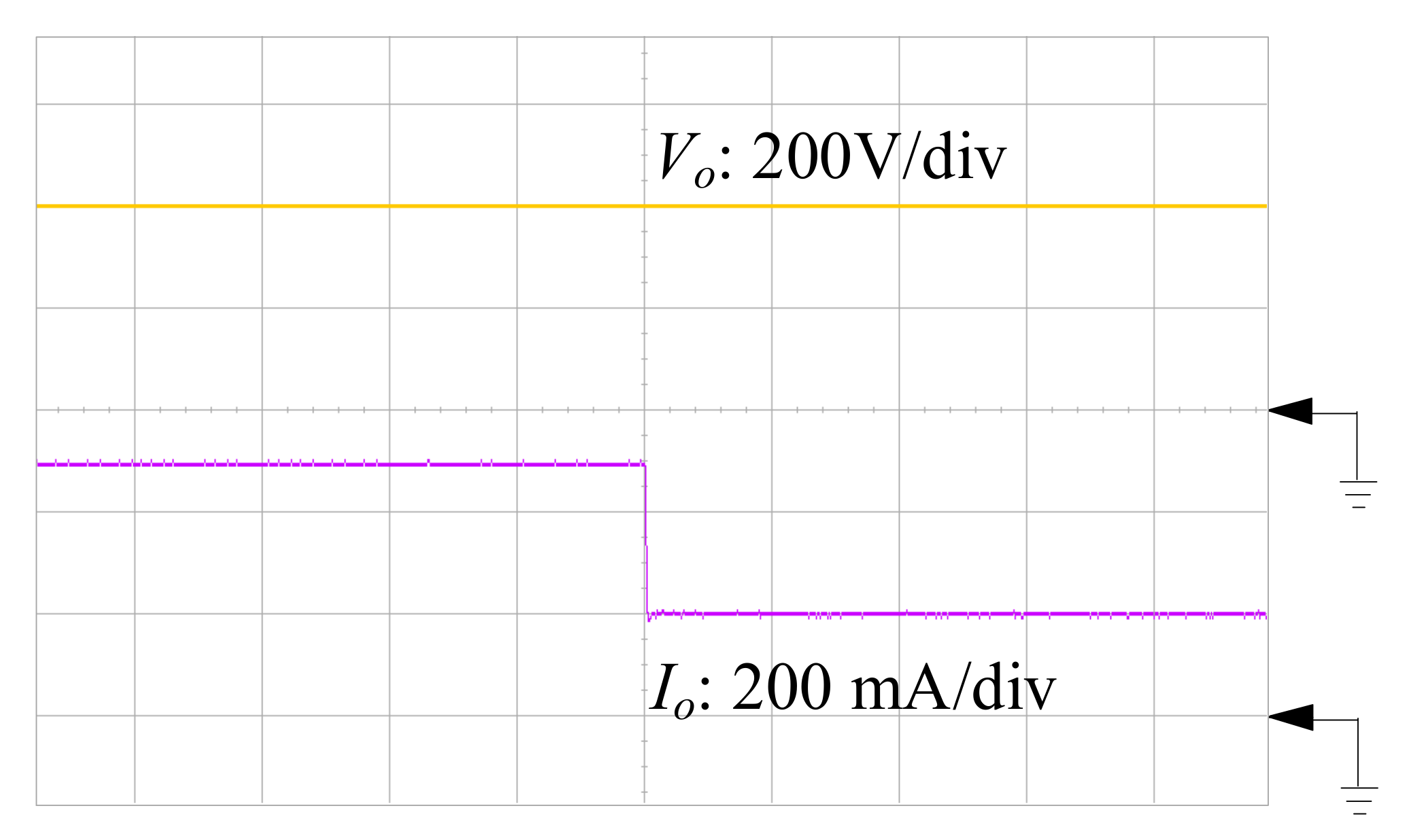
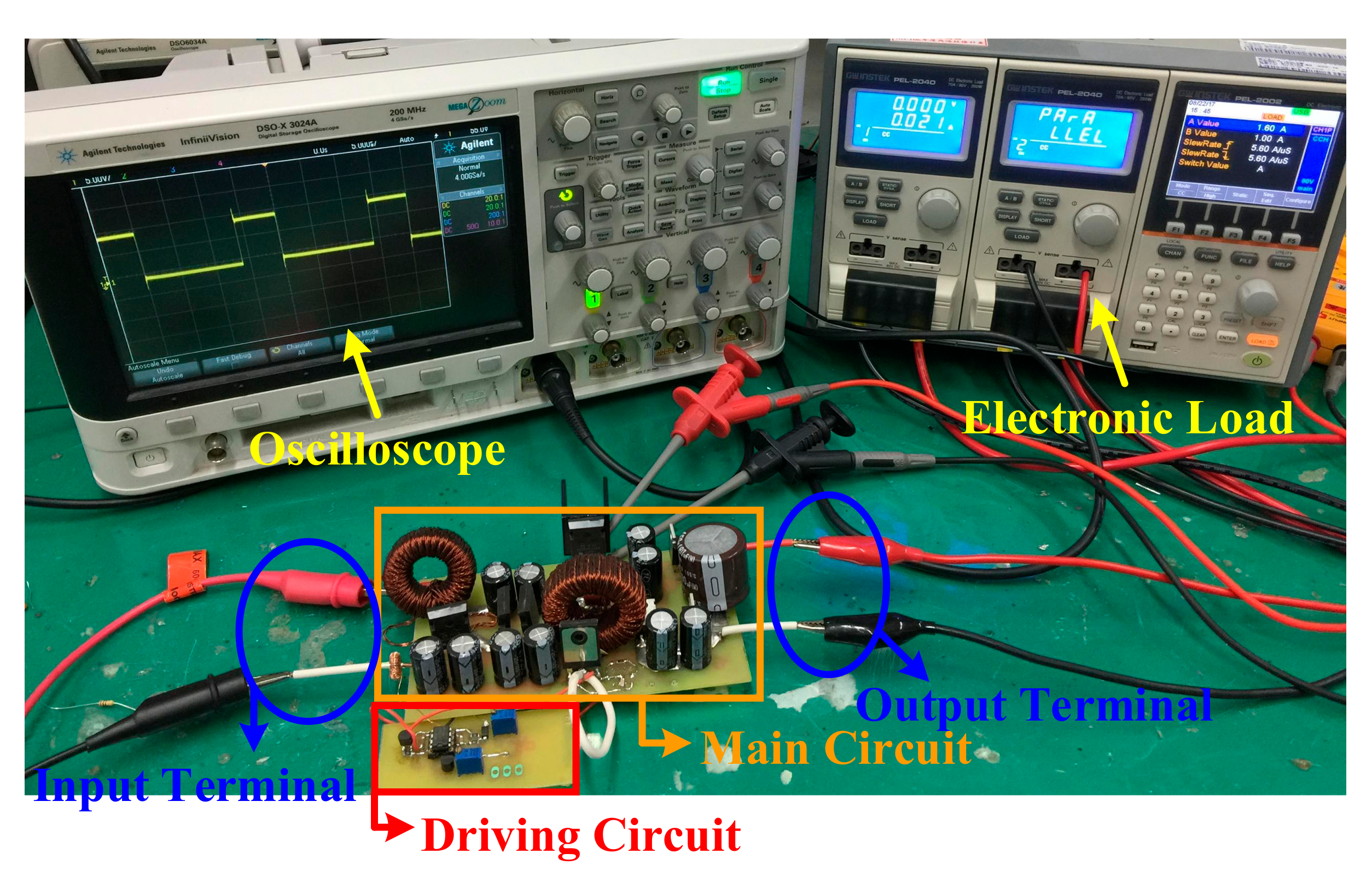
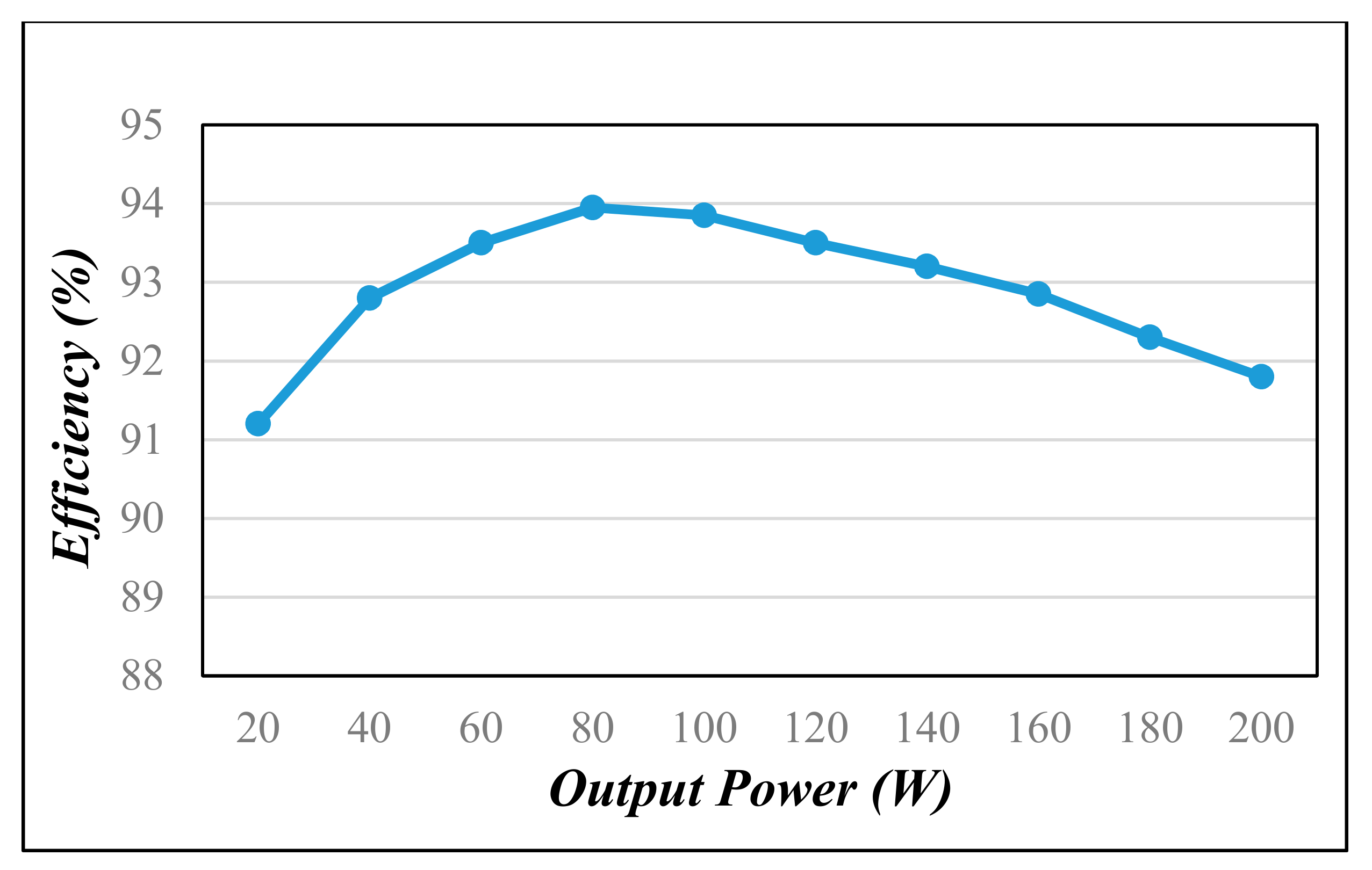
6. Experimental Results
7. Conclusions
Acknowledgments
Author Contributions
Conflicts of Interest
References
- Zhang, Y.; Shi, J.; Zhou, L.; Li, J.; Sumner, M.; Wang, P.; Xia, C. Wide input-voltage range boost three-level DC-DC converter with quasi-Z source for fuel cell vehicles. IEEE Trans. Power Electron. 2017, 32, 6728–6738. [Google Scholar] [CrossRef]
- Kefalas, T.D.; Kladas, A.G. Analysis of transformers working under heavily saturated conditions in grid-connected renewable-energy systems. IEEE Trans. Ind. Electron. 2012, 59, 2342–2350. [Google Scholar] [CrossRef]
- Yang, B.; Li, W.; Zhao, Y.; He, X. Design and analysis of a grid-connected photovoltaic power system. IEEE Trans. Power Electron. 2010, 25, 992–1000. [Google Scholar] [CrossRef]
- Cao, Y.; Samavatian, V.; Kaskani, K.; Eshraghi, H. A novel nonisolated ultra-high-voltage-gain DC-DC converter with low voltage stress. IEEE Trans. Ind. Electron. 2017, 64, 2809–2819. [Google Scholar] [CrossRef]
- Shen, C.-L.; Chiu, P.-C.; Lee, Y.-C. Novel interleaved converter with extra-high voltage gain to process low-voltage renewable-energy generation. Energies 2016, 9, 871. [Google Scholar] [CrossRef]
- Wong, Y.-S.; Chen, J.-F.; Liu, K.-B.; Hsieh, Y.-P. A novel high step-up DC-DC converter with coupled inductor and switched clamp capacitor techniques for photovoltaic systems. Energies 2017, 10, 378. [Google Scholar] [CrossRef]
- Wu, Y.-E.; Wu, Y.-L. Design and implementation of a high efficiency, low component voltage stress, single-switch high step-up voltage converter for vehicular green energy systems. Energies 2016, 9, 772. [Google Scholar] [CrossRef]
- Lu, Y.; Xing, Y.; Wu, H. A PWM plus phase-shift controlled interleaved isolated boost converter based on semiactive quadrupler rectifier for high step-up applications. IEEE Trans. Ind. Electron. 2016, 63, 4211–4221. [Google Scholar] [CrossRef]
- Nguyen, M.K.; Lim, Y.C.; Choi, J.H.; Cho, G.B. Isolated high step-up DC-DC converter based on quasi-switched-boost network. IEEE Trans. Ind. Electron. 2016, 63, 7553–7562. [Google Scholar] [CrossRef]
- Tseng, S.-Y.; Wang, H.-Y. A photovoltaic power system using a high step-up converter for DC load applications. Energies 2013, 6, 1068–1100. [Google Scholar] [CrossRef]
- Shen, C.-L.; Chen, H.-Y.; Chiu, P.-C. Integrated three-voltage-booster DC-DC converter to achieve high voltage gain with leakage-energy recycling for PV or fuel-cell power systems. Energies 2015, 8, 9843–9859. [Google Scholar] [CrossRef]
- Pinto, R.; Mariano, S.; Calado, M.; de Souza, J. Impact of rural grid-connected photovoltaic generation systems on power quality. Energies 2016, 9, 739. [Google Scholar] [CrossRef]
- Li, W.; Li, W.; He, X.; Xu, D.; Wu, B. General derivation law of nonisolated high-step-up interleaved converters with built-in transformer. IEEE Trans. Ind. Electron. 2012, 59, 1650–1661. [Google Scholar] [CrossRef]
- Ajami, A.; Ardi, H.; Farakhor, A. A novel high step-up DC/DC converter based on integrating coupled inductor and switched-capacitor techniques for renewable energy applications. IEEE Trans. Power Electron. 2015, 30, 4255–4263. [Google Scholar] [CrossRef]
- Yan, Z.; Ai-ming, S. Simplified ferrite core loss separation model for switched mode power converter. IET Power Electron. 2016, 9, 529–535. [Google Scholar] [CrossRef]
- Yan, Z.; Qimi, C.; Junbo, Z. Predicting core losses under the DC bias based on the separation model. IEEE J. Emerg. Sel. Top. Power Electron. 2017, 5, 833–840. [Google Scholar] [CrossRef]
- Han, Y.; Liu, Y.F. A practical transformer core loss measurement scheme for high-frequency power converter. IEEE Trans. Ind. Electron. 2008, 55, 941–948. [Google Scholar] [CrossRef]
- Barg, S.; Ammous, K.; Mejbri, H.; Ammous, A. An improved empirical formulation for magnetic core losses estimation under nonsinusoidal induction. IEEE Trans. Power Electron. 2017, 32, 2146–2154. [Google Scholar] [CrossRef]
- Steinmetz, C.P. On the law of hysteresis. Proc. IEEE 1984, 72, 196–221. [Google Scholar] [CrossRef]


| Symbols | Values & Types |
|---|---|
| Vin (input voltage) | 24 V |
| Vo (Output Voltage) | 400 V |
| Po (output power) | 200 W |
| fs (switch frequency) | 50 kHz |
| n1, n2 (transformer turns ratio) | 1 |
| Lm11 (magnetizing inductance) | 70.4 μH |
| Lm21 (magnetizing inductance) | 70.6 μH |
| Llk11 (Leakage inductance) | 1.45 μH |
| Llk21 (Leakage inductance) | 1.45 μH |
| C1, C2, C3 (Capacitance) | 47 μF |
| Clk (Capacitance) | 5 μF |
| C4, C5 (Capacitance) | 100 μF |
| Co (Capacitance) | 220 μF |
| S1 (Switch) | IRFP4332PbF |
| D1 | SBL6045PT |
| D2, D3, Dlk (Diodes) | DSSK60-02AR |
| D4, D5, Do (Diodes) | BYV34 |
| Current Probe | Tektronix TCP312, 30ADL |
|---|---|
| Power Supply | iDRC CDSP-060-100C |
| Oscilloscope | Agilent DSO-X 3024A 200MHz 4GSa/s |
| DC Load | GW Instek PEL-2041 0 A/10 A 2.5 V/500 V 350 W |
| LCR Meter | MICROTEST 6377 |
© 2017 by the authors. Licensee MDPI, Basel, Switzerland. This article is an open access article distributed under the terms and conditions of the Creative Commons Attribution (CC BY) license (http://creativecommons.org/licenses/by/4.0/).
Share and Cite
Shen, C.-L.; Liou, H. Magnetic Material Assessment of a Novel Ultra-High Step-Up Converter with Single Semiconductor Switch and Galvanic Isolation for Fuel-Cell Power System. Materials 2017, 10, 1311. https://doi.org/10.3390/ma10111311
Shen C-L, Liou H. Magnetic Material Assessment of a Novel Ultra-High Step-Up Converter with Single Semiconductor Switch and Galvanic Isolation for Fuel-Cell Power System. Materials. 2017; 10(11):1311. https://doi.org/10.3390/ma10111311
Chicago/Turabian StyleShen, Chih-Lung, and Heng Liou. 2017. "Magnetic Material Assessment of a Novel Ultra-High Step-Up Converter with Single Semiconductor Switch and Galvanic Isolation for Fuel-Cell Power System" Materials 10, no. 11: 1311. https://doi.org/10.3390/ma10111311
APA StyleShen, C.-L., & Liou, H. (2017). Magnetic Material Assessment of a Novel Ultra-High Step-Up Converter with Single Semiconductor Switch and Galvanic Isolation for Fuel-Cell Power System. Materials, 10(11), 1311. https://doi.org/10.3390/ma10111311