

Article

Three-Bridge LLC Resonant Converter with 5 Operation Mode Transitions for Wide Output Voltage Control

1
Department of Electrical and Electronics Engineering, Jeonju University, Jeonju 55069, Republic of Korea
2
Research Institute of Engineering and Technology, Jeonju University, Jeonju 55069, Republic of Korea
3
Department of Mechanical and Automotive Engineering, Jeonju University, Jeonju 55069, Republic of Korea
*
Author to whom correspondence should be addressed.
Energies 2026, 19(3), 590; https://doi.org/10.3390/en19030590
Submission received: 26 November 2025 / Revised: 9 January 2026 / Accepted: 21 January 2026 / Published: 23 January 2026
(This article belongs to the Special Issue Optimization of DC-DC Converters and Wireless Power Transfer Systems)

Abstract

This paper presents a 3-Bridge LLC resonant converter featuring wide output voltage gain characteristics and a novel control method. To achieve operation within a narrower frequency control range, the proposed converter introduces one additional operational mode compared to the previously suggested 3-bridge topology. The converter is configured to have five distinct operation modes, controlled by the switching patterns of the main switches, to enable wide-range output voltage regulation. In each mode, frequency modulation is employed for output voltage control. Furthermore, a morphing control strategy is utilized to ensure stable output voltage regulation during mode transitions. The validity and practical applicability of the proposed 3-bridge LLC resonant converter with five operation modes are verified through experimental results from a 6 kW prototype.

1. Introduction

The utilization of electric motors and batteries is rapidly increasing across various applications, including the automotive industry and industrial mobility devices, as they replace conventional internal combustion engines. In particular, the demand for E-mobility solutions such as electric golf carts and electric forklifts has grown, requiring battery packs with diverse nominal voltages depending on the application. Consequently, this necessitates procuring individual chargers tailored to each specific battery pack voltage. A more practical solution, however, is the development of chargers featuring Zero Voltage Switching (ZVS) DC-DC converters with a wide output voltage control range to accommodate various battery packs [1,2]. Recently, a great deal of research has focused on developing ZVS LLC resonant converters to support the charging of various devices [3,4,5,6].
In several prior studies, various main circuit topologies incorporating relays or MOSFETs on the secondary side of the converter have been proposed to achieve a wide voltage gain range [7,8,9,10,11]. However, these proposed topologies suffer from transient phenomena during mode transitions, which are caused by abrupt variations in voltage gain. While the study presented in [12] enables a wide output voltage range without employing additional switching elements on the secondary side, it faces limitations in the achievable output voltage range because two transformers are permanently connected in series on the secondary side. However, due to the inherent gain characteristics of the LLC resonant tank, where the output voltage gain becomes flat above the resonant frequency, the conventional ZVS LLC resonant converter struggles to achieve a wide output voltage control range. Improving the gain typically requires an excessive reduction in the transformer’s magnetizing inductance, which unfortunately increases the conduction losses in the primary-side switching devices and the transformer, thereby degrading efficiency. To achieve a moderately wide output voltage control range (approximately two-fold), LLC resonant converters employing the morphing control technique have been proposed. These converters implement mode conversion between Half-Bridge (HB) and Full-Bridge (FB) topologies, utilizing frequency modulation (FM) and Duty Modulation (DM) to ensure stable output voltage control during significant gain changes and mode transitions [12,13,14,15]. Nevertheless, these LLC converters are limited in their ability to operate with a voltage control range exceeding four times. To address the challenge of charging diverse battery pack voltages (12–96 VDC), we have previously proposed a 3-Bridge LLC resonant converter [16]. The 3-bridge LLC resonant converter operates across four operation modes from Primary-Series Secondary-Parallel (PSSP) HB to Primary-Parallel Secondary-Series (PPSS) FB to extend the voltage gain range. To maintain ZVS operation and facilitate morphing control, an excessively small magnetizing inductance is required, which inevitably incurs high conduction losses and transformer heating. Furthermore, a critical drawback emerges during the transition from Mode 2 to Mode 3, where the switching frequency shifts to unacceptably high values, particularly failing to achieve the required gain reduction under light-load conditions. Building upon the previous work reported in [16], this paper presents an enhanced control scheme for a three-bridge LLC resonant converter. The proposed approach introduces an additional operating mode by configuring a hybrid HB/FB structure between the two resonant tanks. As demonstrated in the subsequent sections, the proposed strategy achieves a wide output voltage range from 7.5 to 120 VDC while significantly narrowing the required switching frequency range, without reducing the magnetizing inductance. The effectiveness of the proposed scheme is experimentally verified using a 6-kW prototype.
The remainder of this paper is organized as follows. Section 2 presents the structure and operational characteristics of the proposed resonant converter. This section provides a detailed analysis of the operating modes and gain characteristics, followed by a description of the morphing control scheme for operating mode transitions and the DSP control block implementation. Section 3 demonstrates the experimental results obtained from a 6-kW prototype of the 3-bridge LLC resonant converter. These results encompass not only steady-state performance but also the system’s response under abrupt voltage fluctuation scenarios. Finally, Section 4 concludes the paper.

2. A 3-Bridge LLC Resonant Converter Featuring Five Operational Modes

This section consists of two parts: the operational principles of the proposed converter for each mode and the morphing control strategy for seamless mode transitions. The proposed converter comprises six switches and operates in five distinct modes that define the current flow paths according to specific switching patterns. In the first subsection, the operational mechanism of each mode and its corresponding gain characteristics are discussed. The second subsection describes a mode transition strategy utilizing morphing control to meet diverse output voltage requirements. This morphing control technique simultaneously regulates the frequency and duty cycle of the PWM signals that drive the switching devices. Additionally, a detailed description of the DSP control block used to implement this strategy is provided.

2.1. Structure and Operational Characteristics of the 3-Bridge LLC Resonant Converter

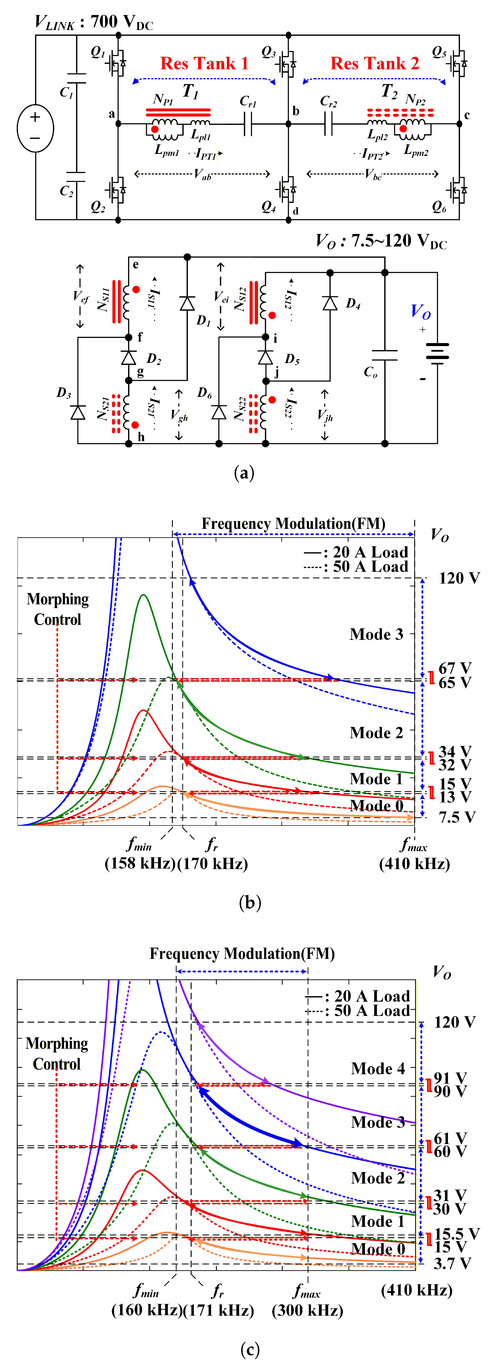
The topology of the proposed 3-bridge LLC resonant converter and its corresponding voltage gain characteristics are depicted in Figure 1. The voltage gain is determined by the operating frequency and load, as expressed in Equations (1)–(5). Specifically, Figure 1b,c display the gain curves for loads of 20 A (solid lines) and 50 A (dashed lines), where the distinct colors represent the gain profiles across different operational modes as a function of frequency.
The proposed 3-bridge LLC resonant converter in Figure 1a is configured on the primary side with six main switching devices ( Q 1 to Q 6 ) for mode transition and switching frequency control, and primary windings ( N P = N P 1 , N P 2 ) connected to two transformers ( T 1 , T 2 ) with their respective primary leakage inductances ( L p l = L p l 1 , L p l 2 ) and magnetizing inductances ( L p m = L p m 1 , L p m 2 ). The resonant capacitors ( C r = C r 1 , C r 2 ) are also connected in series, forming two distinct primary resonant tanks, henceforth referred to as Res. Tank 1 and Res. Tank 2. The secondary side is connected to the center-tapped secondary windings ( N S = N S 11 , N S 12 , N S 21 , N S 22 ) of T 1 and T 2 , which have identical turn ratios, followed by the output rectifier diodes ( D 1 to D 6 ).
Figure 1b presents a schematic gain curve adopted for comparative purposes, highlighting the distinctions between the previous study [16] and the current work, particularly regarding the number of employed modes and the resulting frequency control range. As shown in Figure 1b, the operation of the previously proposed 3-bridge LLC resonant converter in [16], designed for a wide input-output voltage regulation range, transitions between four operational modes (as illustrated by Mode 0, Mode 1, Mode 2, Mode 3) based on the switching patterns of the six main switching devices ( Q 1 / Q 2 , Q 3 / Q 4 , Q 5 / Q 6 ). Depending on the mode, the primary side operates as a series or parallel half-bridge, or a series or parallel full-bridge, while the secondary side is connected in series or parallel based on transformer polarity. The resulting four modes determine the input-output voltage gain. Each mode transition utilizes morphing control, which combines FM and DM for mode transition, followed by subsequent FM to achieve a wide output voltage control range ( V o : 7.5 VDC to 120 VDC). However, as depicted in Figure 1b, the FM range required for the topology mode transition between Mode 2 and Mode 4 was excessively wide. This presented a problem, particularly under light-load conditions, where the required gain regulation range could not be reached, hindering proper mode transition. To address this issue, as shown in Figure 1c, one additional mode (designated as Mode 3) was introduced between the existing Mode 2 and Mode 3 (shown in Figure 1b) to enable topology mode transition within a narrower frequency control range.
This newly defined mode, termed Mode 3, involves Res. Tank 1 operating in a FB configuration and Res. Tank 2 operating in a HB switching configuration. By adding one more mode to the morphing control (which simultaneously utilizes FM and DM), the 5-mode LLC resonant converter can achieve mode transition within a significantly reduced variable frequency control range compared to the conventional 4-mode LLC resonant converter [16]. This made it possible to increase the transformer magnetizing inductance ( L m : 205.3   μ H / 207.8   μ H 291.1   μ H / 288.5   μ H ) while maintaining the wide output voltage control range ( V o : 7.5   VDC 120   VDC ), ultimately resulting in improved efficiency.

2.1.1. Operation and Gain Characteristics ( G v 0 , G v 1 ) of Mode 0 and Mode 1

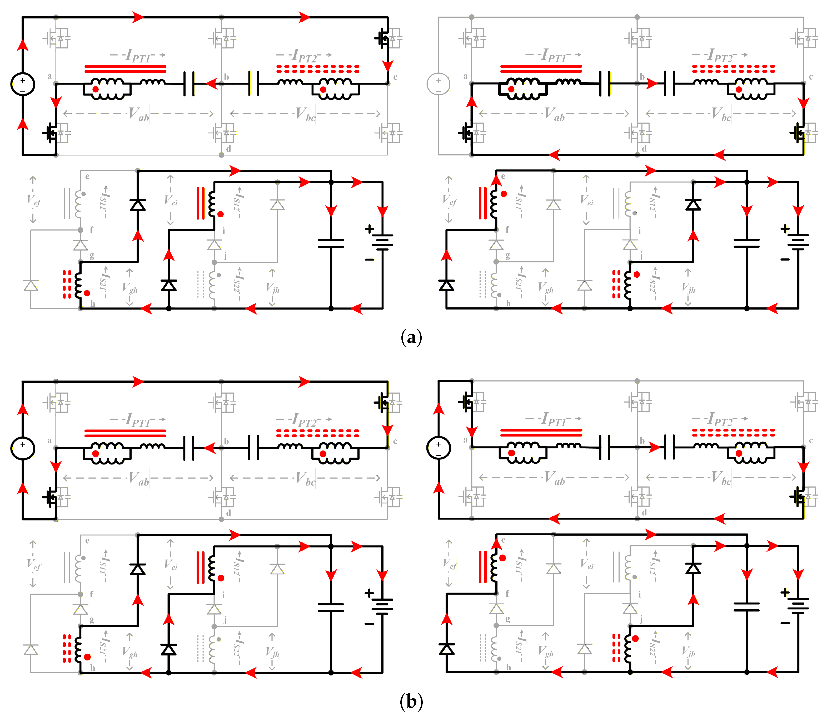
In Mode 0 (PSSP HB Operation), the main switching device Q 2 is perpetually turned on, while Q 1 , Q 3 , and Q 4 are turned off. Q 5 and Q 6 execute the switching operation with a 50% duty cycle every period. Consequently, as shown in Figure 2a, the two primary resonant tanks (i.e., Res. Tank 1 and Res. Tank 2) of the main circuit are connected in series, and the secondary windings of the transformer are connected in parallel based on the transformer polarity. This configuration operates as a HB to deliver power to the secondary side, hence the designation PSSP HB Operation. As indicated in Table 1, with a nominal battery pack voltage ( V o ) of 12   VDC taken as the reference for Mode 0, the output voltage can be controlled from the minimum battery pack voltage of 7.5   VDC (≈1/2 V o ) up to 15   VDC or higher (≈2 V o ) through FM.
In Mode 1 (PSSP FB Operation), the main switching devices Q 3 and Q 4 are turned off, while the pairs ( Q 2 , Q 5 ) and ( Q 1 , Q 6 ) execute the switching operation mutually exclusively with a 50% duty cycle every period. As shown in Figure 2b, similar to Mode 0, the resonant tanks (Res. Tank 1 and Res. Tank 2) are connected in series on the primary side and parallel on the secondary side. However, this mode achieves power transfer over a higher gain range through FB operation (i.e., PSSP FB Operation). Accordingly, with a nominal battery pack reference voltage of 24   VDC for Mode 1, the output voltage can be controlled from a minimum of 15   VDC (≈ 2 V o ) up to 30   VDC or higher (≈ 4 V o ).
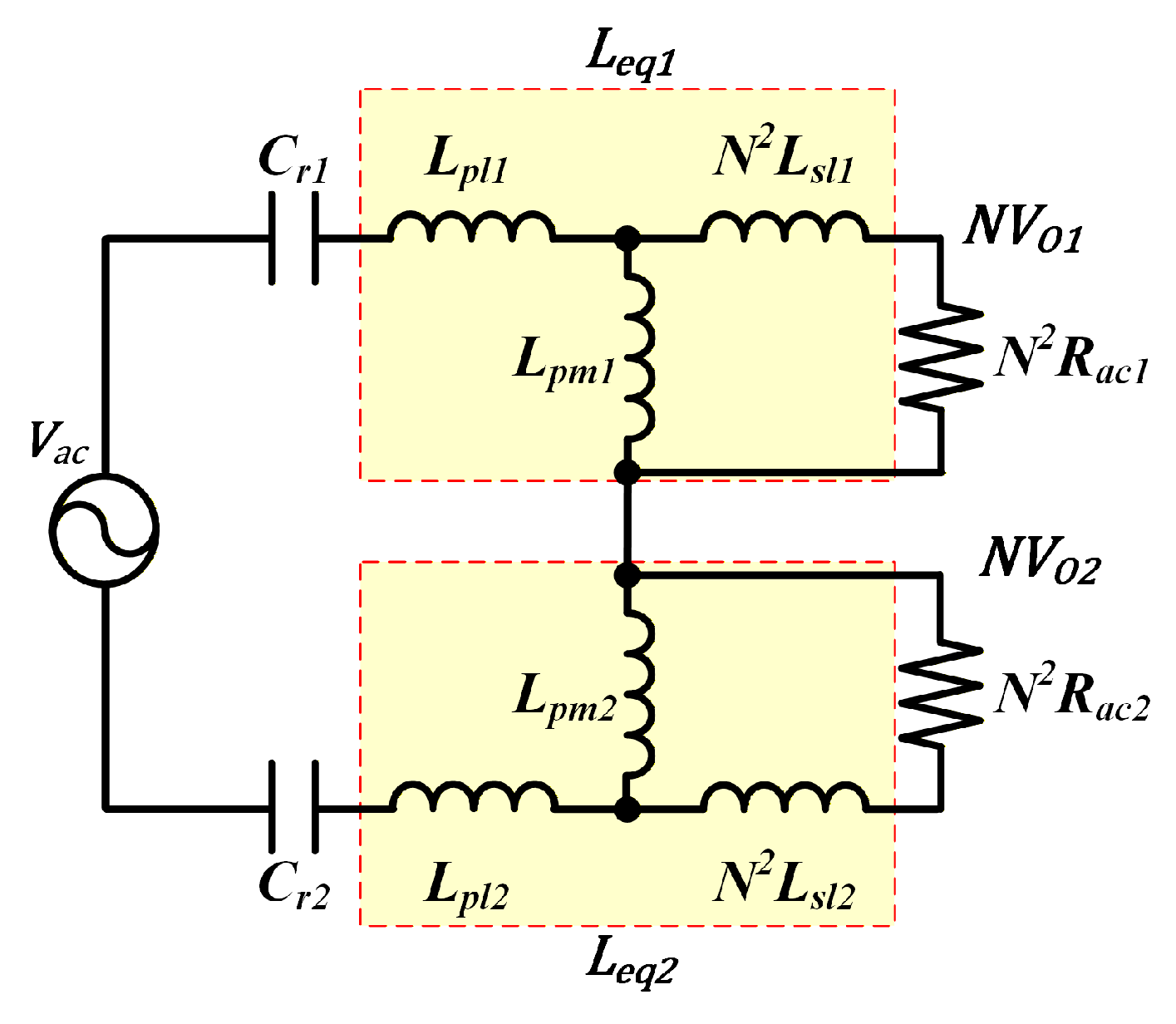
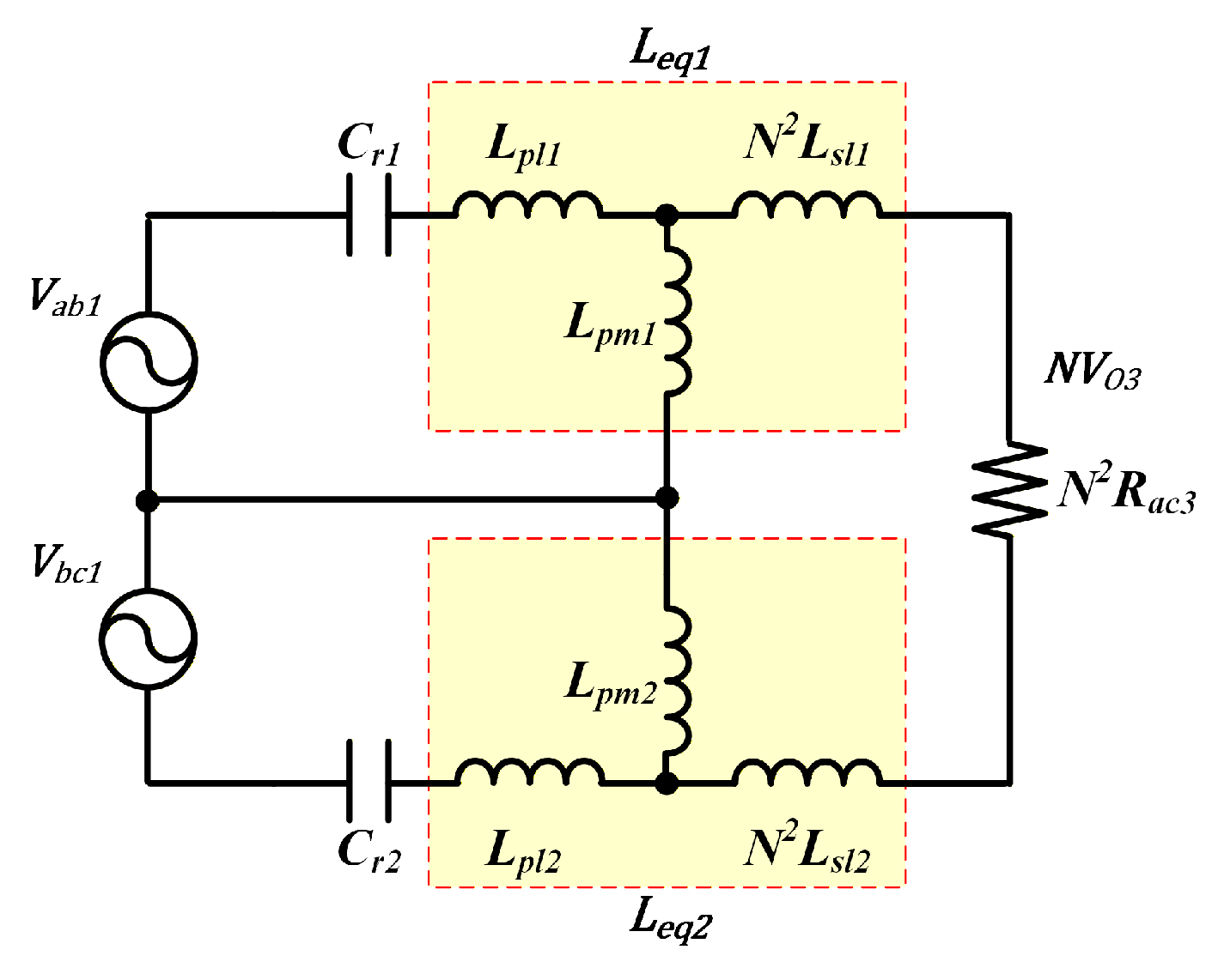
Figure 3 illustrates the simplified AC equivalent model for Mode 0 and Mode 1 of the proposed 3-bridge LLC resonant circuit. The model comprises the primary and secondary leakage inductances ( L p l = L p l 1 , L p l 2 and L s l = L s l 1 , L s l 2 ), the magnetizing inductances ( L p m = L p m 1 , L p m 2 ), the resonant capacitors ( C r = C r 1 = C r 2 ), and the secondary equivalent AC load resistance ( R a c = 8 R d c / π 2 ). The resonant capacitor C r is the primary-side resonant capacitor tuned to the resonant frequency ( f r ) compensated by the equivalent leakage inductance L e q . R a c converts the DC load resistance ( R d c ) into an equivalent AC resistance. The voltage gain characteristics of the 3-bridge LLC resonant circuit were analyzed using the Fundamental Harmonic Approximation (FHA) method. Only the fundamental harmonics are considered, and the 3rd, 5th, and 7th harmonics are neglected when applying the method. The resulting gain equations are presented in Equations (1) and (2). For the simplification of analysis, it is assumed that the parameter values for the two resonant circuits (Res. Tank 1 and Res. Tank 2) are identical.
G v 0 = 1 2 · 1 2 1 + A 1 ω n 2 A + B 1 + B + j Q a ( 1 + B ) ω n 2 1 ω n ,
G v 1 = 1 2 1 + A 1 ω n 2 A + B 1 + B + j Q a ( 1 + B ) ω n 2 1 ω n ,
where A = L p 1 / L p m , B = N 2 L s 1 / L p m , Q a = 2 ω r L e q / N 2 R a c . ω r = 1 / L e q C r , ω n = ω / ω r . ω = 2 π f . f is the switching frequency. L p l = L p l 1 = L p l 2 , L p m = L p m 1 = L p m 2 , N 2 L s l = N 2 L s l 1 = N 2 L s l 2 , N = N P / N S , L e q = L e q 1 = L e q 2 , L e q = L p l + ( L p m / / N 2 L s l ) = L p m ( A + B 1 + B ) , C r = C r 1 = C r 2 , and R a c = R a c 1 = R a c 2 . It is noted that the quality factor Q a serves as a key parameter in defining the dynamic performance and gain characteristics of the LLC resonant converter.

2.1.2. Mode 2, Mode 3, and Mode 4 Operations and Gain Characteristics ( G v 2 , G v 3 , G v 4 )

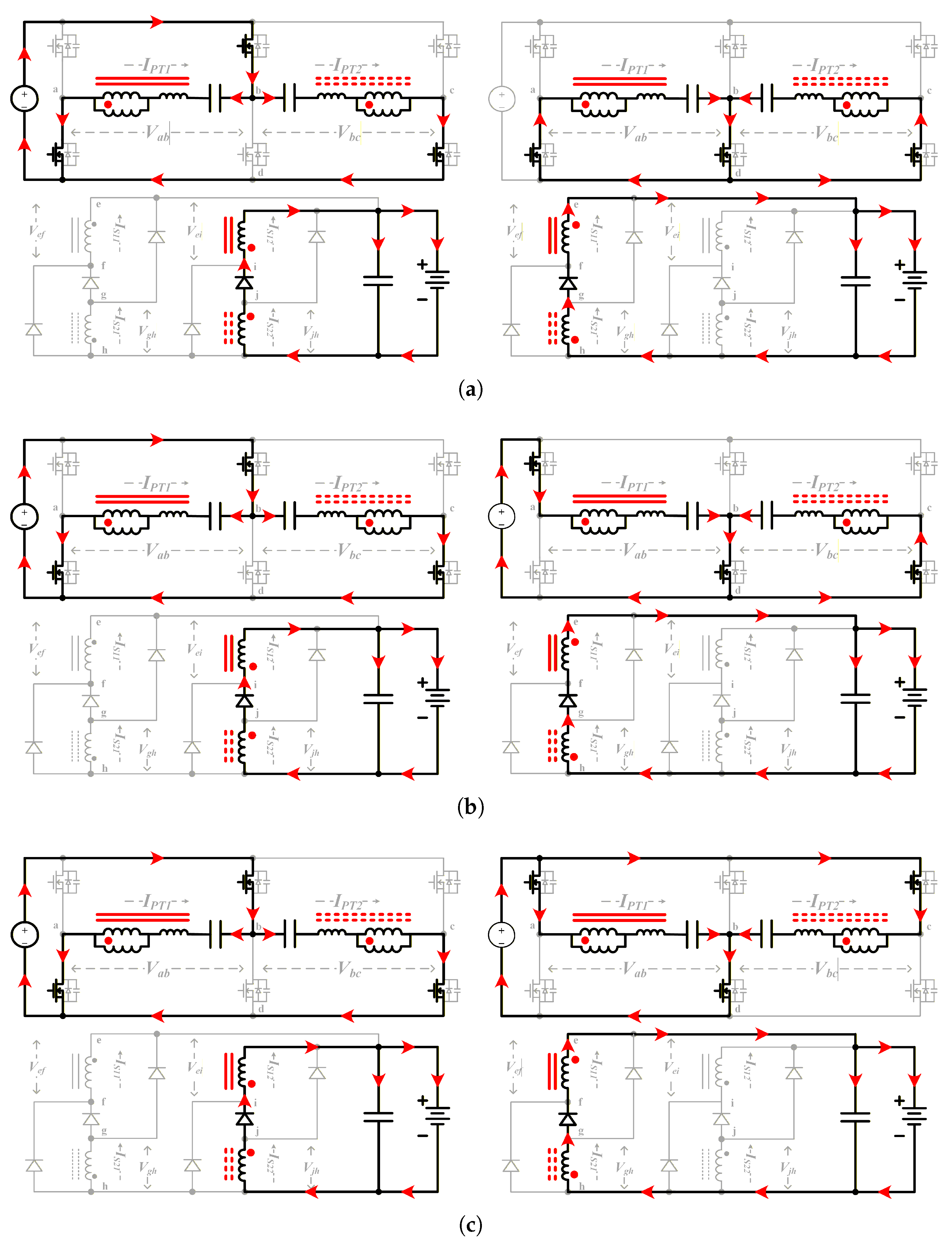
In Mode 2, the main switching devices Q 2 and Q 6 are turned on, while Q 1 and Q 5 are consistently turned off. Under this condition, Q 3 and Q 4 perform a turn-on/turn-off switching operation with a 50 % duty cycle in every period. Consequently, as illustrated in Figure 4a, the two primary-side resonant circuits (Res. Tank 1 and Res. Tank 2) are connected in parallel, and the secondary transformer windings are connected in series based on the transformer polarity. This is the PPSS HB operation mode, which transfers power through half-bridge operation. In this mode, output voltage control is achievable from the minimum voltage of a 48   VDC rated battery pack (i.e., 30   VDC ) up to 8   V o ( 60   VDC or more).
In Mode 3, the main switching device Q 6 is turned on and Q 5 is turned off. The pairs ( Q 1 / Q 4 ) and ( Q 2 / Q 3 ) perform turn-on/turn-off switching operations with a 50 % duty cycle in every period. Thus, as shown in Figure 4b, Res. Tank 1 operates with FB switching, while Res. Tank 2 operates with HB switching. Although the primary-side circuits operate in a parallel connection, the secondary-side windings are connected in series based on the transformer polarity. This is the PPSS Hybrid (FB-HB) Operation, where each resonant tank (Res. Tank 1 and Res. Tank 2) supplies power to the load according to its respective gain characteristics. Therefore, output voltage control is possible from a minimum voltage of 8   V o (i.e., 60   VDC ) up to 12   V o ( 90   VDC or more) for a 72   VDC rated battery pack.
In Mode 4, the main switching pairs ( Q 1 / Q 4 / Q 5 ) and ( Q 2 / Q 3 / Q 6 ) perform turn-on and turn-off switching with a 50 % duty cycle in every period. Consequently, as depicted in Figure 4c, the two primary-side resonant circuits (Res. Tank 1 and Res. Tank 2) are connected in parallel and perform FB switching, and the secondary transformer windings are connected in series according to the transformer polarity. This operation is referred to as the PPSS FB operation. This mode enables output voltage control up to 16   V o ( 120   VDC or more) for a 96   VDC rated battery pack.
In Mode 2, 3, and 4 operations, the two primary-side resonant circuits ( Res .   Tank   1 and Res .   Tank   2 ) are connected in parallel, and the secondary transformer windings are connected in series according to the transformer polarity. The equivalent circuit for this configuration is shown in Figure 5. By applying the principle of superposition, the gain equations for each operating mode are derived and presented in Equations (3)–(5). Again, for the simplification of analysis, it is assumed that the parameter values for the two resonant circuits (Res. Tank 1 and Res. Tank 2) are identical.
G v 2 = 1 1 + A 1 ω n 2 A + B 1 + B + j 2 Q b ( 1 + B ) ω n 2 1 ω n ,
G v 3 = 3 2 · 1 1 + A 1 ω n 2 A + B 1 + B + j 2 Q b ( 1 + B ) ω n 2 1 ω n ,
G v 4 = 2 · 1 1 + A 1 ω n 2 A + B 1 + B + j 2 Q b ( 1 + B ) ω n 2 1 ω n ,
where A = L p 1 / L p m , B = N 2 L s 1 / L p m , Q b = ω r L e q / N 2 R a c . ω r = 1 / L e q C r , ω n = ω / ω r . ω = 2 π f . f is the switching frequency. L p l = L p l 1 = L p l 2 , L p m = L p m 1 = L p m 2 , N 2 L s l = N 2 L s l 1 = N 2 L s l 2 , N = N P / N S , L e q = L e q 1 = L e q 2 , L e q = L p l + ( L p m / / N 2 L s l ) = L p m ( A + B 1 + B ) , C r = C r 1 = C r 2 , and R a c = R a c 3 .
In Mode 0, the minimum voltage of the 12   V battery is 10.5   V , which can potentially cause the switching frequency to increase to the maximum frequency ( f m a x ) under light-load conditions. Since the primary-side transformers are connected in series, a voltage of V L I N K / 2 ( 350   V ) is applied. Therefore, considering the secondary-side leakage inductance ( N 2 L s l ) reflected to the primary side, as expressed in Equation (6), the transformer magnetizing inductance ( L p m _ Z V S ) must be less than or equal to 463.6   μ H .
L p m _ Z V S N V o t d e a d 8 · C O S S V i n f m a x N 2 L s l ,
where t d e a d denotes the dead time and is set to 300 ns, and C O S S represents the MOSFET output capacitance, which is set to 112 pF in this work. f m a x is set to 300 kHz.
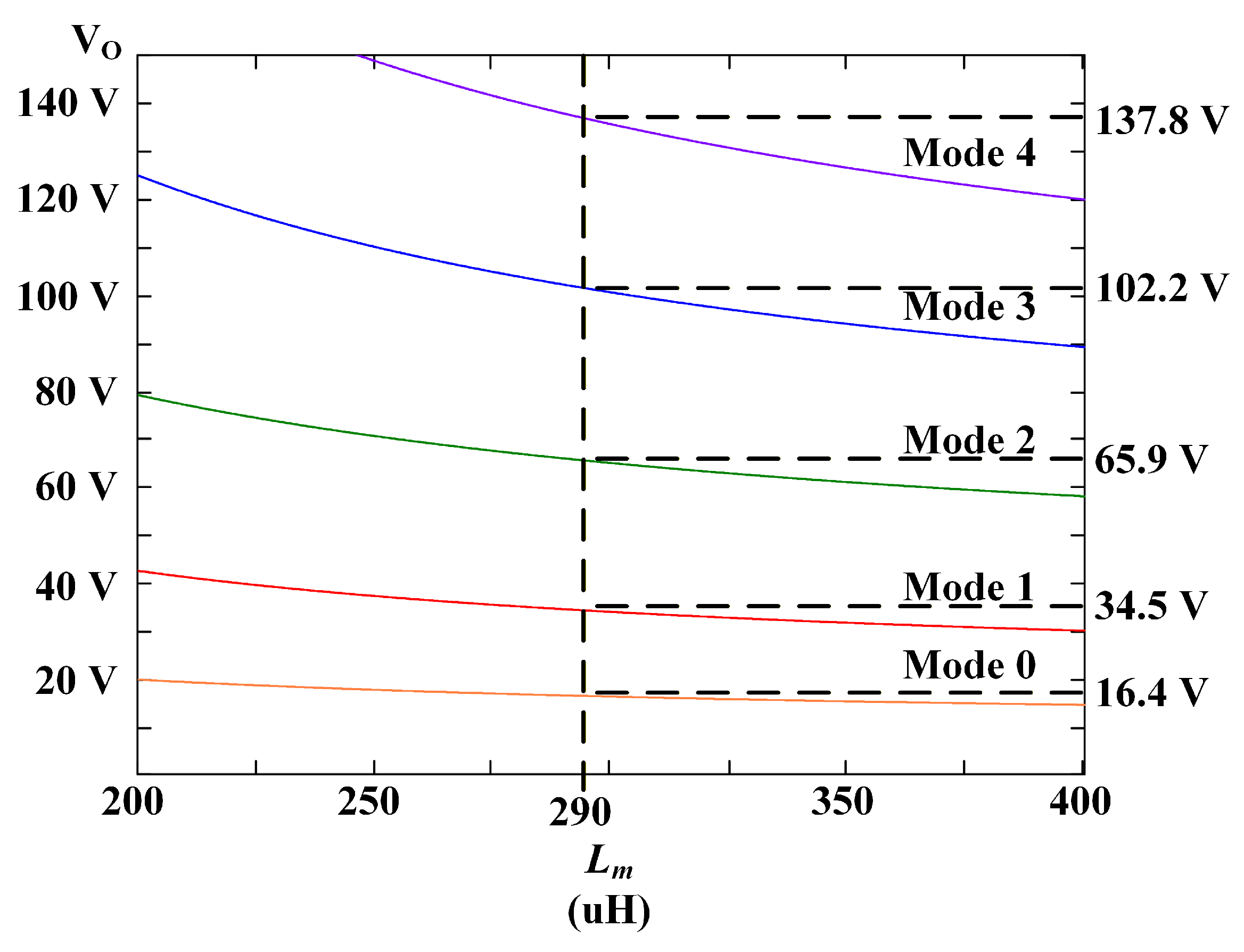
To enable operating mode transitions, the L p m value must be adjusted to satisfy the mode-transition output voltage conditions for each mode. Figure 6 illustrates the output voltage ( V o ) gain characteristics as a function of L p m variation at the minimum switching frequency ( f s = 160   kHz ), where L p m is selected to find the desired gain that meets the output voltage control criteria, as referenced by the L p m terms ( A , B , and   Q ) in Equations (1) through (5). Accordingly, the maximum L p m value that satisfies the upper band (UB) required for mode transition can be confirmed through the gain characteristics shown in Figure 6. Considering the voltage drop across the secondary-side diodes, the transformer magnetizing inductance ( L p m ) was applied such that the output voltage in Mode 0 is approximately 1   V higher than the UB (i.e., 15.5   V ). Since the voltage must be 31   V , 61   V , and 91   V or more for Mode 1, Mode 2, Mode 3, and Mode 4, respectively, at the minimum switching frequency ( f m i n ), the magnetizing inductance ( L p m ) was selected as 290   μ H , which satisfies the UB of all modes. As this value is smaller than the 463.6   μ H obtained from Equation (6), it satisfies both the required voltage gain for mode transition and the ZVS condition.
Based on these criteria, the transformer parameters were selected by adjusting the transformer air gap. Considering the equivalent leakage inductance ( L e q = L e q 1 = L e q 2 ), the resonant capacitors were selected and are presented in Table 2. The gain characteristics for each operating mode are shown in Figure 1c, confirming that mode transition is possible across the desired output voltage ( V o ) control range.

2.2. Morphing Control for Operating Mode Transition

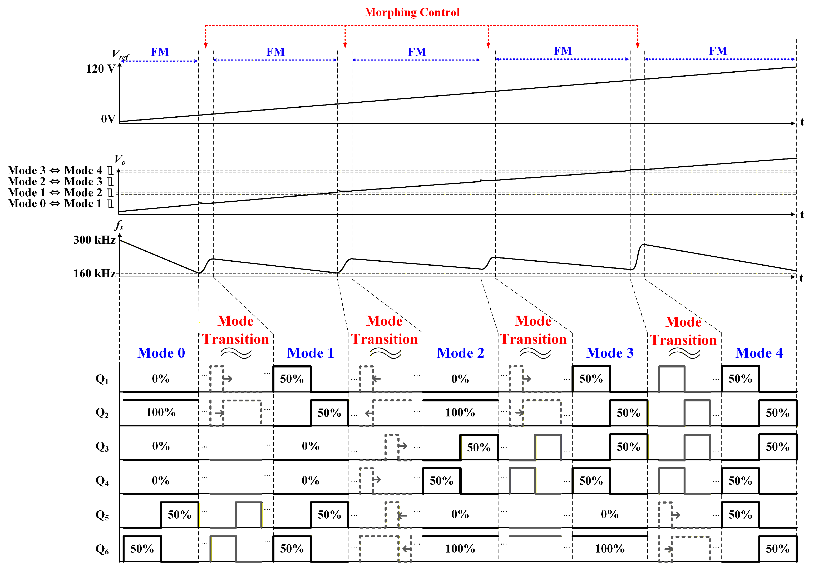
The main circuit proposed in this paper operates in five distinct modes, as described in Section 2.1, thereby achieving a wide output voltage control range of 7.5   VDC to 120   VDC . The mode transition process can be conceptually understood by referring to Figure 1c and Figure 7. Consider a specific operational scenario as follows: when a battery requiring a charge is connected to the converter, control initiates in the mode capable of providing the battery’s present voltage (e.g., Mode 2). In this state, the system tracks the target voltage by navigating the gain curve of the corresponding mode via frequency control. Once the current output voltage reaches the predefined threshold for mode transition (refer to Table 1), a transition to the subsequent mode (e.g., Mode 3) is triggered. To implement a switching pattern identical to that of the target mode, duty cycle control is executed. During this phase, any potential rise in output voltage resulting from the pattern change is suppressed by simultaneous frequency control, ensuring a stable and seamless transition. If the output voltage ( V o ) were controlled solely by variable switching frequency control (i.e., FM), the voltage gain would change abruptly during each mode transition, potentially causing a transient state in the output voltage ( V o ) and output current ( I o ). Therefore, a morphing control scheme—where variable switching frequency control and duty control are simultaneously applied—was adopted to ensure stable and precise control of the output voltage ( V o ) even during the mode transition intervals.
To define the band gaps in Table 1 used for the morphing control intervals, the parameters listed in Table 2 were applied, and the gain characteristic curves of each operating mode (shown in Figure 1c) were considered. Note that this gain curve corresponds to L p m = 290   μ H.
The mode transition must be achievable under constant current load conditions of 5   A and 50   A . The output voltage control ranges for each mode were determined based on the gain characteristic curve simulations (see Figure 1c), satisfying the required battery pack charging voltage range as follows: Mode 0, 7.5   VDC to 15.5   VDC ; Mode 1, 15   VDC to 31   VDC ; Mode 2, 30   VDC to 61   VDC ; Mode 3, 60   VDC to 91   VDC ; and Mode 4, 90   VDC to 120   VDC . However, segmenting the operating modes based on a single voltage threshold carries the risk of malfunction during mode transitions. This risk was mitigated by implementing band gaps between the segments. The band gaps applied to each mode transition interval are divided into a UB and a Lower Band (LB), as shown in Table 1, Figure 7 and Figure 8. The operation upon reaching a band gap is determined by both the current operating mode and the previous cycle’s operating mode.
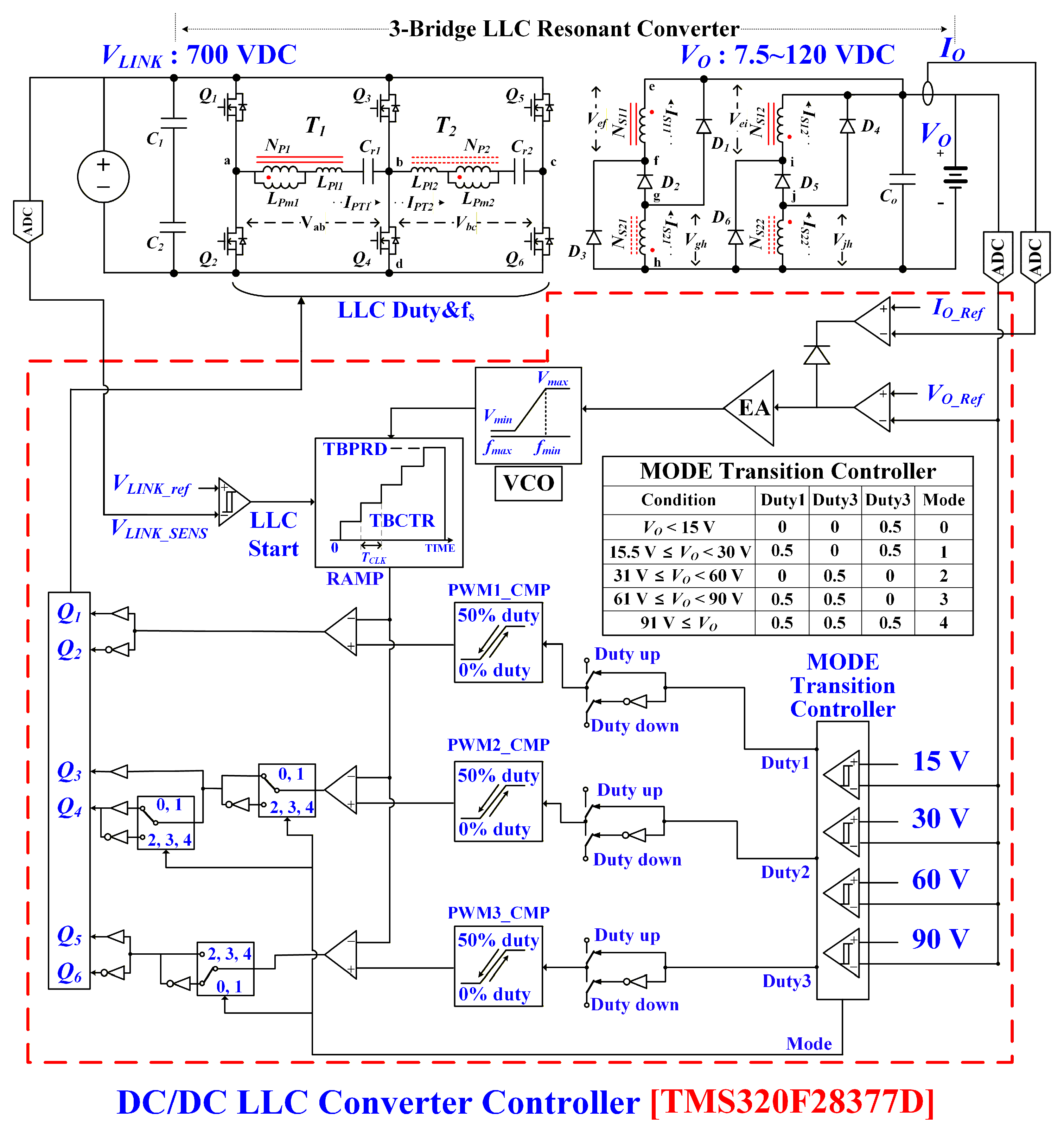
As illustrated in Figure 8, the reference control voltage V o _ R e f and the feedback output voltage V o are compared and passed through an Error Amplifier (EA), and then the switching frequency ( f s ) is determined via a voltage-controlled oscillator (VCO). Consequently, the TBPRD (Time-Base Period) value is determined by T s (Switching Period) divided by T C L K (DSP chip’s clock period) within the RAMP block. The mode transition controller receives the feedback output voltage V o and, based on the per-mode voltage range conditions (as shown in the internal table of Figure 8), determines the operating mode as well as the values for Duty1, Duty2, and Duty3. A hysteresis band gap voltage of 0.5   V is applied between Mode 0 and Mode 1, while a 1   V band gap is applied across the remaining mode transition intervals. As indicated in Table 1 and Figure 1c, a transition to the next mode is initiated only when the condition V o UB is satisfied, and a transition to the previous mode is initiated when the condition V o < LB is satisfied.
The mode transition controller outputs the operating mode along with the Duty1, Duty2, and Duty3 values as a function of the output voltage V o , as illustrated in Figure 8. Since the switching pattern of the switching devices varies across each operating mode, the system executes distinct actions based on the resulting Duty1, Duty2, and Duty3 values provided by the controller. Specifically, an output value of 0.5 for Duty1, Duty2, and Duty3 initiates a duty cycle ramp-up (0% → 50%), whereas an output value of 0 initiates a duty cycle ramp-down (50% → 0%), thereby modulating the values of PWM1_CMP, PWM2_CMP, and PWM3_CMP. The ON/OFF signals for the switching devices are determined by comparing PWM1_CMP, PWM2_CMP, and PWM3_CMP with the TBCTR (Time-Base Counter) value of the RAMP block via comparators. The mode transition controller further decides whether to invert the switching signal for each switch based on the output Mode value. Therefore, during a mode transition, as shown in Figure 7, the duty cycle of the switching devices ( Q 1 to Q 6 ) is smoothly increased or decreased to change to the switching pattern appropriate for the new mode. As depicted in Figure 8, the switching frequency f s is controlled through PI control by comparing V o _ R e f with V o and I o _ R e f with I o , ensuring the output voltage reaches the target reference voltage V o _ R e f even during the mode transition intervals.
Under the proposed morphing control scheme, the mode transition process takes place. Consequently, the proposed morphing control during mode transition is a hybrid control method where variable switching frequency control and duty control are simultaneously performed. This technique prevents transient states during the mode transition interval, enabling stable output voltage control. This morphing control was implemented using the TMS320F28377D MCU from Texas Instruments.

3. Experimental Results

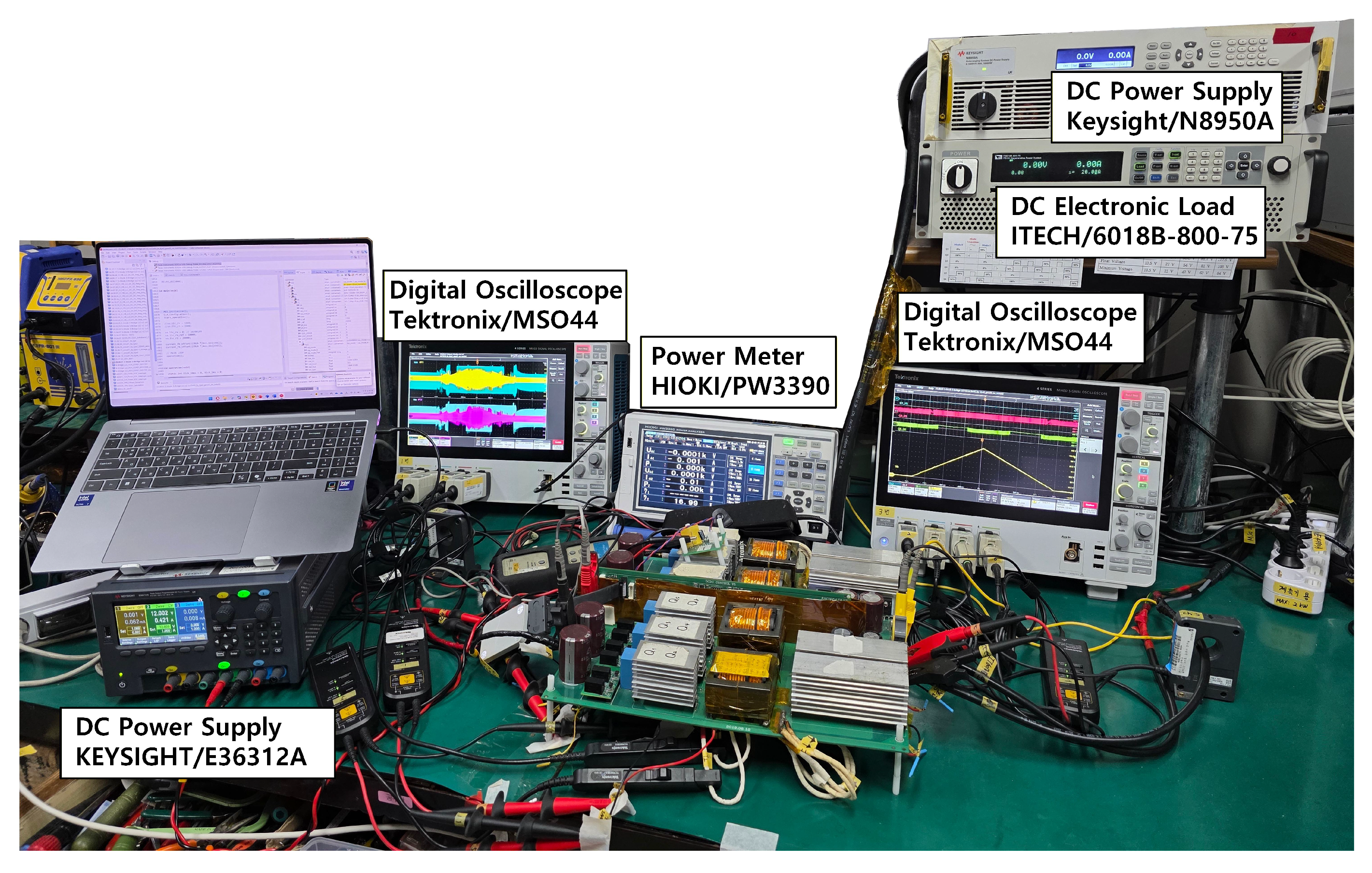
In this paper, a prototype of a 3-bridge LLC resonant converter with a maximum power rating of 6   kW at 120   VDC / 50   A was built and experimentally tested. This converter is designed to operate over a wide output voltage control range ( V o : 7.5 VDC∼120 VDC). The feasibility of this paper was validated by demonstrating that the fabricated prototype, under an input voltage ( V L I N K ) of 700   VDC and the full output voltage control range (7.5 VDC∼120 VDC), successfully achieved control across a wide range ( 3.7   VDC 120   VDC 3.7   VDC ) through the application of the morphing control for five distinct operating mode transitions ( Mode   0 Mode   4 ). Table 3 summarizes the applied input/output specifications and the switching devices used for the experiment. During the experimental setup of the 3-bridge LLC resonant converter, the input power source, as shown in Figure 9, was a DC power supply ( Keysight / N 8950 A / 1000   V / 30   A / 10   kW ), and the output load was an electronic load ( ITECH / IT 6018 - 800 - 75 / 18   kW ). A digital oscilloscope ( Tektronix / MSO 44 ) was used for waveform measurement, and the output power and efficiency were measured using a power meter ( HIOKI / PW 3390 ).
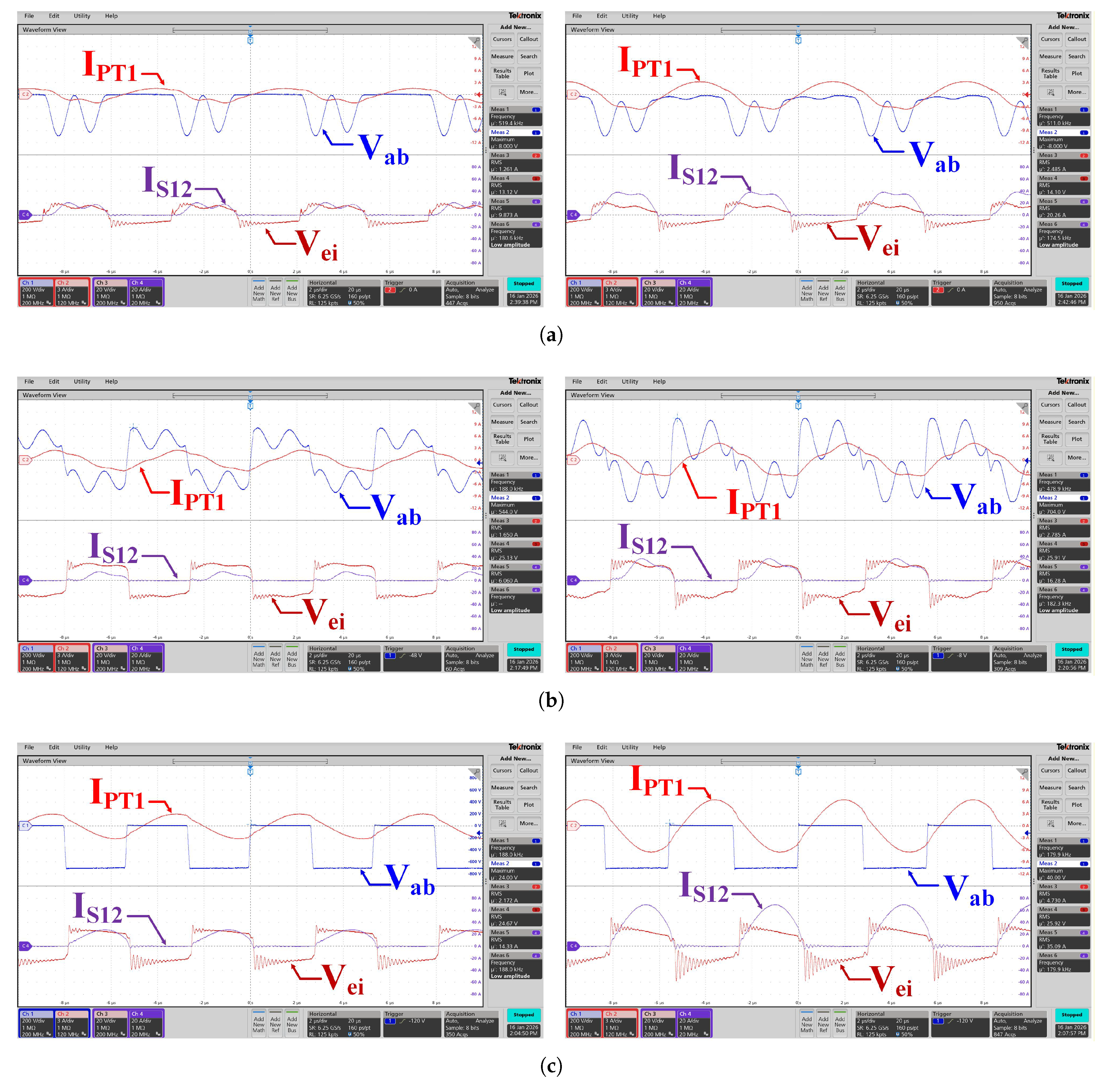
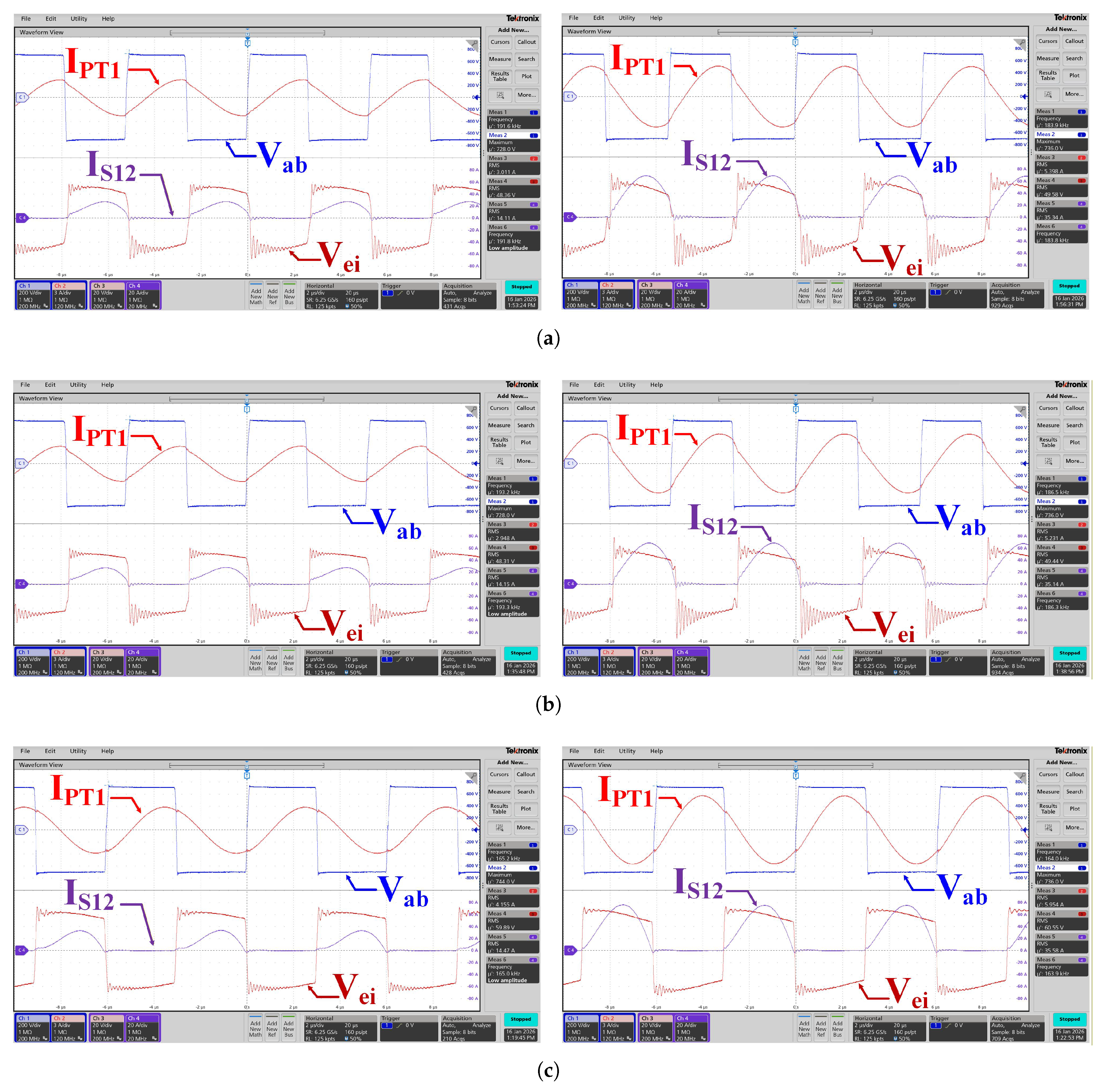
Figure 10 and Figure 11 present the measured waveforms used to verify the ZVS operation under both 20   A and 50   A constant current load conditions across all operating modes (Mode 0∼Mode 4). By observing the phase relationship between the terminal voltage ( V a b ) and the current ( I P T 1 ) of the primary side Res. Tank 1, it was confirmed that ZVS operation is successfully achieved throughout all operating modes and the entire output voltage control range. Specifically, the oscillating waveform observed in the primary side resonant tank terminal voltage ( V a b ) in Mode 0 (shown in Figure 10a) is a parasitic oscillation resulting from the charging and discharging effects of the parasitic capacitance ( C p ) because Q 3 and Q 4 are turned off. This confirms that ZVS operation is sustained even under the 20   A and 50   A constant current load experiments.
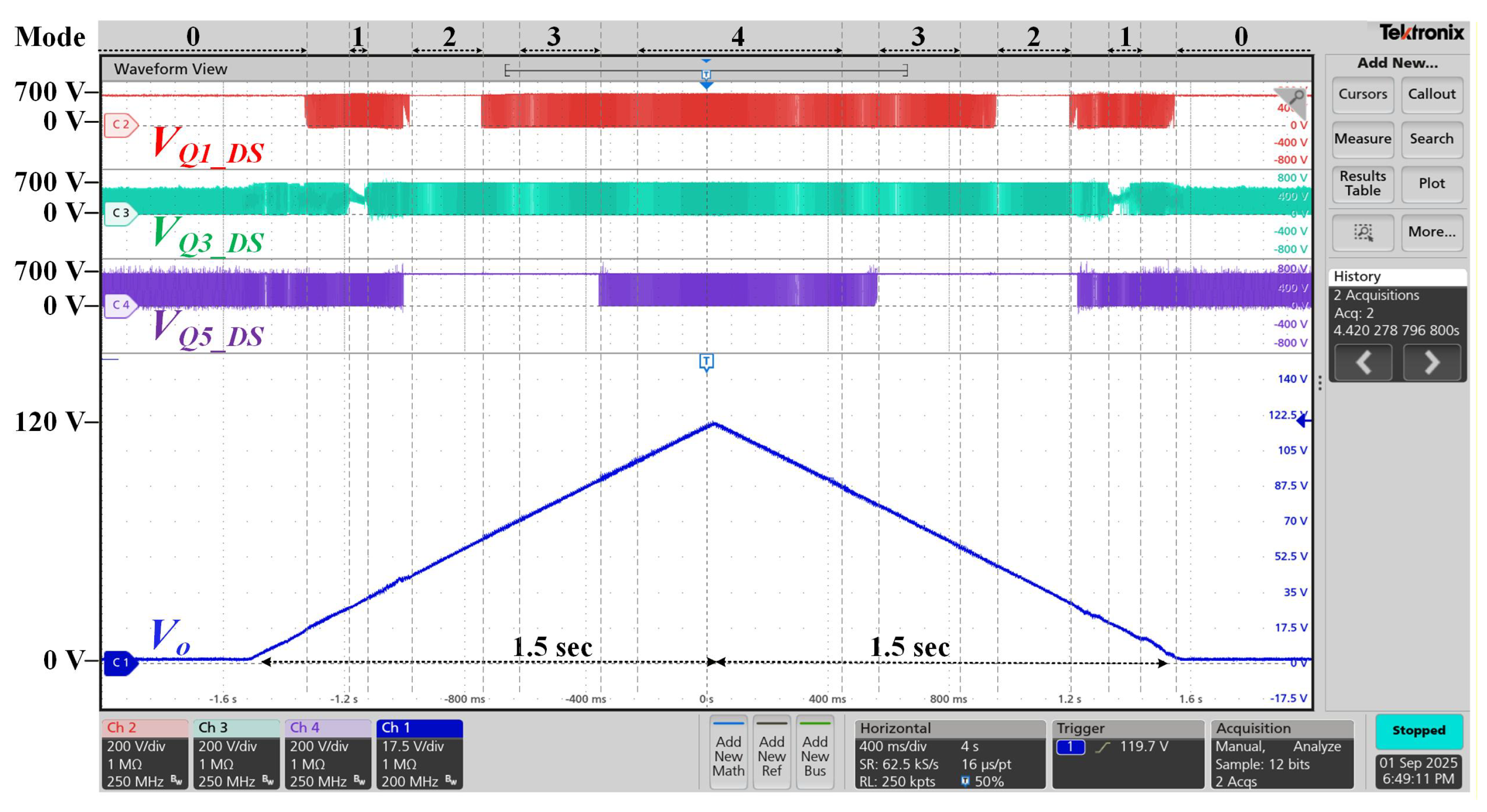
Figure 12 displays the measured waveforms from an experiment conducted by varying the DSP’s output reference voltage ( V o _ R e f ) to verify the continuous operating mode transition for each mode when morphing control is applied. Under a 20   A constant current load condition, as the DSP output reference voltage ( V o _ R e f ) changes over a total duration of 3   s (for both ramp-up and ramp-down), the output voltage ( V o ) is observed to rise from the minimum output voltage ( 3.7   VDC ) to the maximum output voltage ( 120   VDC ) and then fall back over 1.5   s for each phase. During the output voltage rise, mode transitions are initiated when the defined UB threshold for each operating mode is reached as follows: Mode 0 ( 15.5   VDC ), Mode 1 ( 31   VDC ), Mode 2 ( 61   VDC ), and Mode 4 ( 91   VDC ). Conversely, during the output voltage fall, mode transitions are confirmed to occur stably when the defined LB threshold for each operating mode is reached as follows: Mode 0 ( 15   VDC ), Mode 1 ( 30   VDC ), Mode 2 ( 60   VDC ), and Mode 3 ( 90   VDC ). Each mode transition takes 150   ms . During this time, the duty cycle of switch Q 2 changes as follows: Mode 0 (100%), Mode 1 (50%), Mode 2 (100%), Mode 3 (50%), and Mode 4 (50%). This confirms a normal mode transition sequence. Although a transient state in the output voltage ( V o ) is observed during the mode transition intervals between Mode 0 and Mode 1 and between Mode 1 and Mode 2 due to the application of the morphing control, the overall operation is confirmed to be stable and linearly controlled.
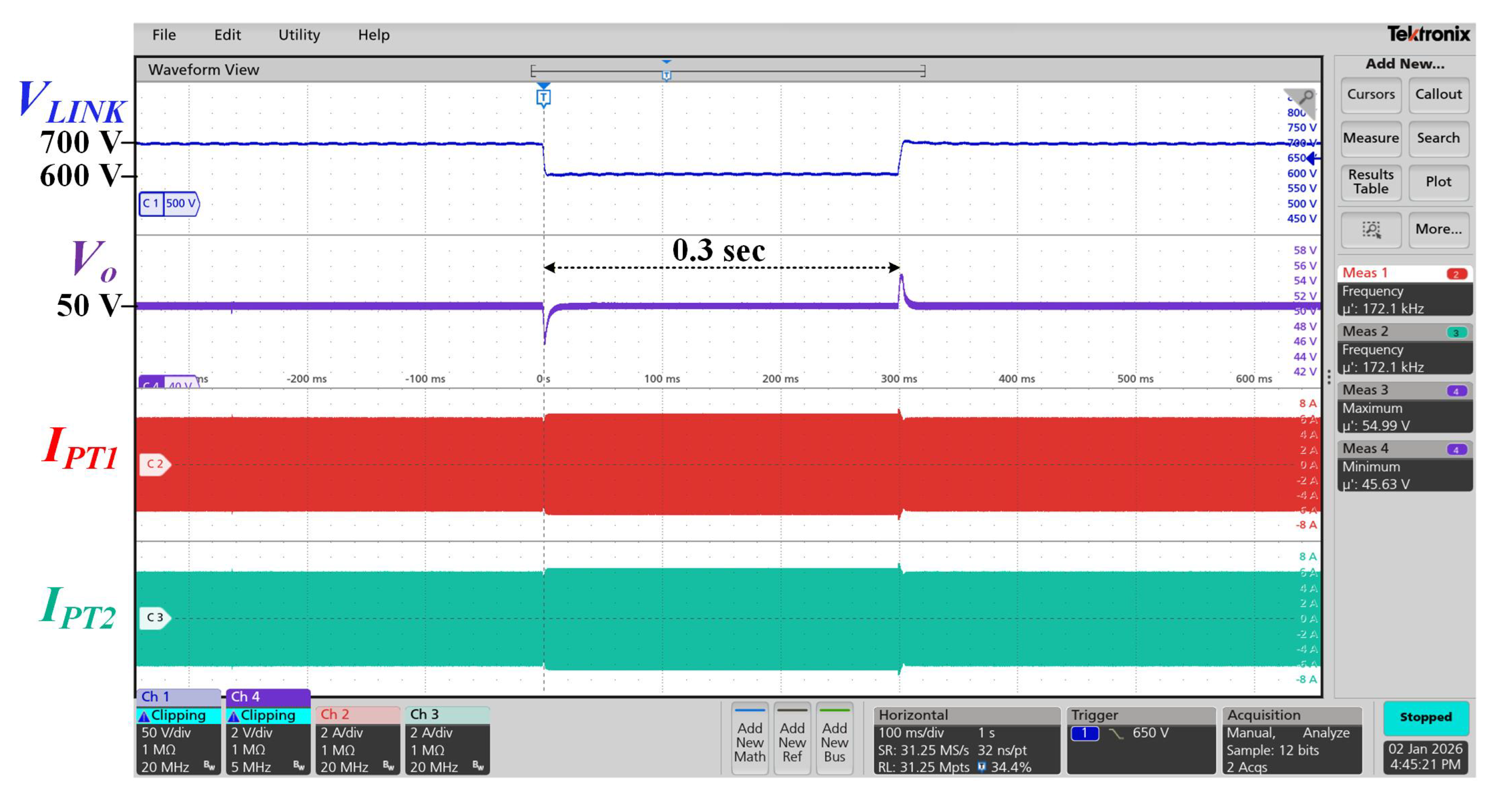
The transient response characteristics during rapid input voltage fluctuation are presented in Figure 13. The experiment was conducted based on a scenario where the input voltage was stepped down from 700 VDC to 600 VDC and then restored to 700 VDC after a 0.3-s interval to observe the resulting overshoot and undershoot in the output voltage. As evidenced by the experimental results, the target output voltage of 50 VDC is stably maintained through variable frequency control. Although fluctuations (within 10% of the target voltage and a recovery time of less than 10 ms) are observed during the transition periods, they are considered within the acceptable operating tolerance for the converter’s application.
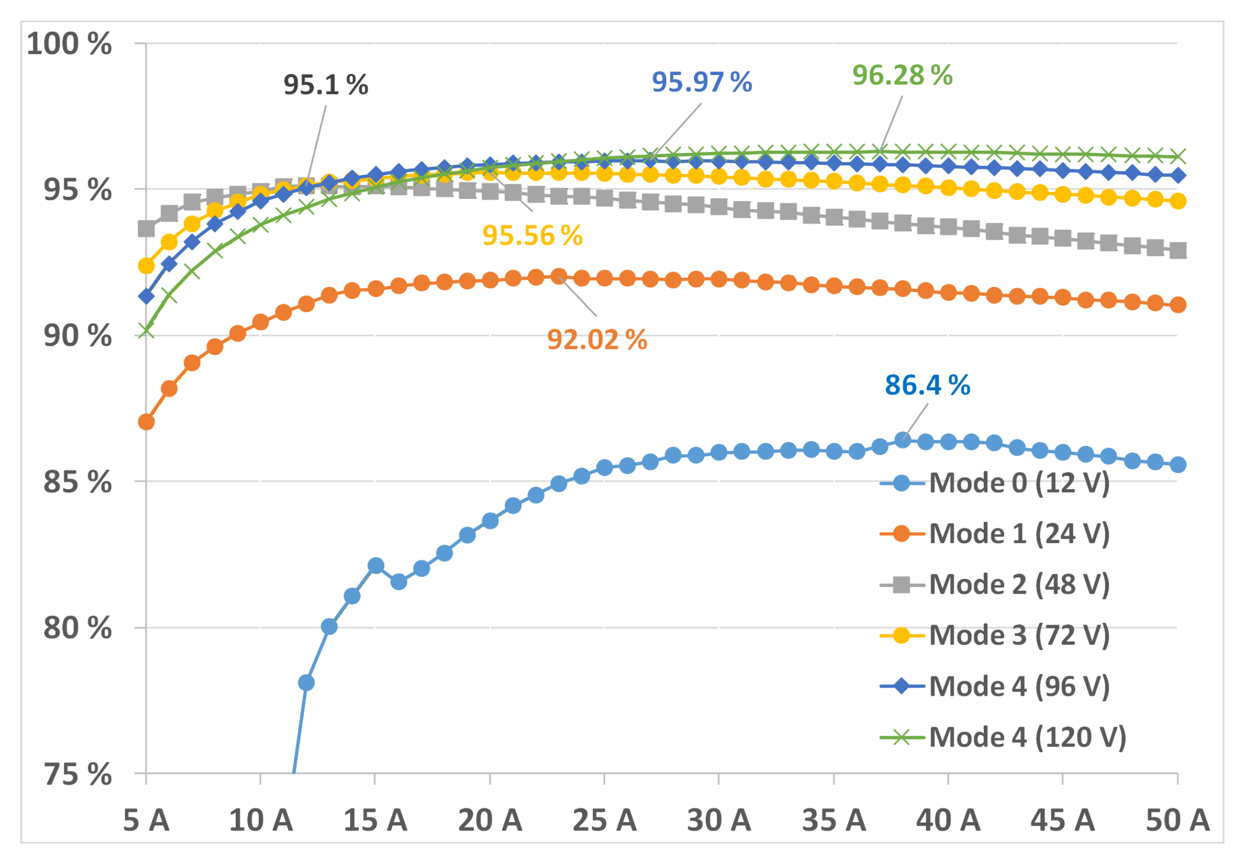
Figure 14 shows the measured efficiency characteristics for each operating mode at the rated voltages ( 12 , 24 , 48 , 96   and   120   VDC ) under constant current load conditions ranging from 5   A to 50   A , increasing in 1   A increments. Due to the low-voltage, high-current operation, Mode 0 exhibits relatively low efficiency characteristics. However, the efficiency performance is observed to improve as the output voltage increases, with a maximum efficiency of 96.28% achieved in Mode 4 at 120   VDC and 37   A . Comparing the efficiency characteristics of each operating mode with the previously published 3-bridge LLC resonant converter with four operating modes [16], the proposed 3-bridge LLC resonant converter shows an efficiency improvement of 0.5∼1%. This enhancement is attributed to the increased magnetizing inductance and the narrower switching control range of the proposed converter.

4. Conclusions

This paper proposed a three-bridge LLC resonant converter designed to accommodate the charging requirements of various battery packs with different rated voltages. The proposed converter operates in five distinct modes based on pre-defined switching patterns, each characterized by unique gain characteristics. To satisfy a wide range of output voltage requirements, mode transitions are inevitably involved. To minimize transients during these transitions, a morphing control technique—integrating frequency modulation (FM) and duty cycle modulation (DM)—was implemented. Once the output voltage meets the transition criteria, the duty cycle of each switch is adjusted linearly to shift toward the target switching pattern. During this process, any fluctuations in the output voltage caused by the switching pattern variation are effectively compensated for through frequency control. For the inherent design limitations of conventional three-bridge LLC resonant converters, specifically, the proposed method overcomes the conventional need to reduce magnetizing inductance for wide output ranges and the requirement for excessively high switching frequencies to achieve lower voltage gains during transitions. By introducing additional operating modes, the proposed converter prevents an excessive increase in the operating frequency range, thereby enhancing overall system efficiency. To verify the comprehensive performance of the proposed converter, a 6-kW prototype was developed and experimentally tested. The viability of the proposed circuit was successfully validated through a detailed performance analysis, including mode-specific operational characteristics, morphing control for seamless transitions, and overall system efficiency.

Author Contributions

E.-s.K. designed the research. J.-w.K., M.-g.K., S.-u.G. and J.-s.P. performed the research, analyzed the data, and wrote the paper. J.-s.W. and J.-h.P. reviewed the paper. All authors have read and agreed to the published version of the manuscript.

Funding

This work was supported by the Korea Institute of Energy Technology Evaluation and Planning (KETEP) and the Ministry of Climate, Energy, Environment (MCEE) of the Republic of Korea. (No. RS-2022-KP002707 and No. RS-2025-07852969).

Data Availability Statement

The raw data supporting the conclusions of this article will be made available by the authors upon request.

Conflicts of Interest

The authors declare no conflicts of interest.

References

  1. Kanimozhi, G.; Kumar, S.S.; Likhitha, K. Battery charger for automotive applications. In Proceedings of the 2016 10th International Conference on Intelligent Systems and Control (ISCO), Coimbatore, India, 7–8 January 2016; pp. 1–6. [Google Scholar] [CrossRef]
  2. Pahlevaninezhad, M.; Das, P.; Drobnik, J.; Jain, P.K.; Bakhshai, A. A Novel ZVZCS Full-Bridge DC/DC Converter Used for Electric Vehicles. IEEE Trans. Power Electron. 2012, 27, 2752–2769. [Google Scholar] [CrossRef]
  3. Beiranvand, R.; Rashidian, B.; Zolghadri, M.R.; Alavi, S.M.H. Using LLC Resonant Converter for Designing Wide-Range Voltage Source. IEEE Trans. Ind. Electron. 2011, 58, 1746–1756. [Google Scholar] [CrossRef]
  4. Deng, J.; Mi, C.C.; Ma, R.; Li, S. Design of LLC Resonant Converters Based on Operation-Mode Analysis for Level Two PHEV Battery Chargers. IEEE/ASME Trans. Mechatron. 2015, 20, 1595–1606. [Google Scholar] [CrossRef]
  5. Deng, J.; Li, S.; Hu, S.; Mi, C.C.; Ma, R. Design Methodology of LLC Resonant Converters for Electric Vehicle Battery Chargers. IEEE Trans. Veh. Technol. 2014, 63, 1581–1592. [Google Scholar] [CrossRef]
  6. Xu, H.; Yin, Z.; Zhao, Y.; Huang, Y. Accurate Design of High-Efficiency LLC Resonant Converter with Wide Output Voltage. IEEE Access 2017, 5, 26653–26665. [Google Scholar] [CrossRef]
  7. Qazi, S.; Venugopal, P.; Watson, A.J.; Wheeler, P.; Soeiro, T.B. Design and Analysis of Reconfigurable Resonant Converter with Ultrawide Output Voltage Range. IEEE Trans. Power Electron. 2024, 39, 5750–5763. [Google Scholar] [CrossRef]
  8. Elezab, A.; Zayed, O.; Abuelnaga, A.; Narimani, M. High efficiency LLC resonant converter with wide output range of 200–1000 V for DC-connected EVs ultra-fast charging stations. IEEE Access 2023, 11, 33037–33048. [Google Scholar] [CrossRef]
  9. Kim, J.W.; Kim, B.; Lee, D.; Cho, Y.; Ji, S.K.; Ryu, D. LLC Resonant Converter for Fast Electric Vehicle Charging Module with a Reconfigurable Bi-Directional Switch. IEEE Trans. Transp. Electrif. 2024, 10, 10169–10181. [Google Scholar] [CrossRef]
  10. Du, B.; Zuo, Y.; Shen, X.; Sui, Q.; Cobaleda, D.B.; Martinez, W. Reconfigurable LLC Resonant Converter for Dual-Architecture EV Charging Systems. In Proceedings of the 2025 Energy Conversion Congress & Expo Europe (ECCE Europe), Birmingham, UK, 1–4 September 2025; pp. 1–4. [Google Scholar] [CrossRef]
  11. Dang, H.; Du, S.; Zhang, Y.; Liu, J. A Novel LLC Resonant Converter with Configurable Capacitors in Output Stage for Wide Output Voltage Range Operation. IEEE Trans. Power Electron. 2022, 37, 6233–6236. [Google Scholar] [CrossRef]
  12. Wei, Y.; Luo, Q.; Alan Mantooth, H. A Novel LLC Converter with Topology Morphing Control for Wide Input Voltage Range Application. IEEE J. Emerg. Sel. Top. Power Electron. 2022, 10, 1563–1574. [Google Scholar] [CrossRef]
  13. Jovanović, M.M.; Irving, B.T. On-the-Fly Topology-Morphing Control—Efficiency Optimization Method for LLC Resonant Converters Operating in Wide Input- and/or Output-Voltage Range. IEEE Trans. Power Electron. 2016, 31, 2596–2608. [Google Scholar] [CrossRef]
  14. Mudiyanselage, G.A.; Kozielski, K.; Emadi, A. Optimal LLC Converter Design with Topology Morphing Control for Wide Voltage Range Battery Charging Applications. IEEE Open J. Power Electron. 2024, 5, 1209–1226. [Google Scholar] [CrossRef]
  15. Zheng, L.; Guo, Y.; Zhao, X.; Wang, R.; Zhang, X.; Lan, L.; Li, H. Morphing control strategy of wide input voltage DR-LLC converter for vehicle power supply. IET Power Electron. 2025, 18, 1209–1226. [Google Scholar] [CrossRef]
  16. Yoo, S.J.; Kim, M.J.; Kim, E.S.; Jeon, Y.S. 3-Bridge LLC resonant converter for achieving wide output voltage control range based on topology morphing. J. Power Electron. 2020, 20, 1420–1432. [Google Scholar] [CrossRef]
Figure 1. Proposed 3-bridge LLC resonant converter. (a) Topology, voltage gain characteristics in 4 operation modes adopted from [16] (b) and 5 operation modes proposed in the work (c). Notes. Colors in the figure represent different modes. Bidirectional arrows indicate the control range of the switching frequency along the gain curve for each specific mode.
Energies 19 00590 g001
Figure 2. Current flows on Mode 0 and Mode 1 in the 3-bridge LLC resonant converter. (a) Current flows on operating Mode 0 and (b) Current flows on operating Mode 1.
Energies 19 00590 g002
Figure 3. Equivalent circuit on Mode 0 and Mode 1 in 3-bridge LLC resonant converter.
Energies 19 00590 g003
Figure 4. Current flows on (a) Mode 2, (b) Mode 3 and (c) Mode 4 in the 3-bridge LLC resonant converter.
Energies 19 00590 g004
Figure 5. Equivalent circuits on Mode 2, Mode 3 and Mode 4 in 3-bridge LLC resonant converter.
Energies 19 00590 g005
Figure 6. Output voltage ( V o ) gain characteristics on operating modes according to L p m at minimum switching frequency ( f s = 160 kHz).
Energies 19 00590 g006
Figure 7. Switching pattern changes in mode transition.
Energies 19 00590 g007
Figure 8. DSP control block diagram of the proposed converter for mode transition (Mode 0 ⇔ Mode 1 ⇔ Mode 2 ⇔ Mode 3 ⇔ Mode 4).
Energies 19 00590 g008
Figure 9. Photograph of experimental setup.
Energies 19 00590 g009
Figure 10. Experimental waveforms in operating modes 0, 1, and 2 [Primary Side Resonant Tank Voltage/Current ( V a b / I P T 1 ), Secondary Side Resonant Tank Voltage/Current ( V e i / I S 12 )] [CH1: 200 V/div, CH2: 3 A/div, CH3: 20 V/div, CH4: 20 A/div]. (a) Mode 0: (L) 12 VDC 20 A (180.6 kHz), (R) 12 VDC 50 A (174.5 kHz); (b) Mode 1: (L) 24 VDC 20 A (188 kHz), (R) 24 VDC 50 A (182.3 kHz); (c) Mode 2: (L) 48 VDC 20 A (188 kHz), (R) 48 VDC 50 A (179.9 kHz).
Energies 19 00590 g010
Figure 11. Experimental waveforms in operating modes 3 and 4 [Primary Side Resonant Tank Voltage/Current ( V a b / I P T 1 ), Secondary Side Resonant Tank Voltage/Current ( V e i / I S 12 )] [CH1: 200 V/div, CH2: 3 A/div, CH3: 20 V/div, CH4: 20 A/div]. (a) Mode 3: (L) 72 VDC 20 A(191.8 kHz), (R) 72 VDC 50 A(183.8 kHz); (b) Mode 4: (L) 96 VDC 20 A(193.2 kHz), (R) 96 VDC 50 A(186.5 kHz); (c) Mode 4: (L) 120 VDC 20 A(165.2 kHz), (R) 120 VDC 50 A(163.9 kHz).
Energies 19 00590 g011
Figure 12. Experimental waveforms on voltage of switching devices ( Q 1 , Q 3 , and Q 5 ) and output voltage ( V o ) due to changing operating modes (load current 20 A) [CH 1: 200 V/div, CH 2: 200 V/div, CH 3: 200 V/div, CH 4: 17.5 V/div].
Energies 19 00590 g012
Figure 13. Experimental waveforms of the output voltage transient response for abrupt input voltage changes from 700 to 600 to 700 VDC (load current 45 A, Mode 3) [CH 1: 50 V/div, CH 2: 2 V/div, CH 3: 2 A/div, CH 4: 2 A/div].
Energies 19 00590 g013
Figure 14. Efficiency characteristics in each operating mode.
Energies 19 00590 g014
Table 1. Bandgap for each operating mode transition.
Mode TransitionBoundsVoltage
Mode 0 ⇔ Mode 1UB 15.5   VDC
LB 15.0   VDC
Mode 1 ⇔ Mode 2UB 31   VDC
LB 30   VDC
Mode 2 ⇔ Mode 3UB 61   VDC
LB 60   VDC
Mode 3 ⇔ Mode 4UB 91   VDC
LB 90   VDC
Table 2. Parameters of transformers and resonant capacitors used in 3-bridge LLC resonant converter.
ParametersValue
Resonant capacitor ( C r 1 / C r 2 ) 6.3   nF / 6.33   nF
Turn ratio ( N P 1 / N S 11 & 12 , N P 2 / N S 21 & 22 )18 (36/2)
Primary leakage inductance ( L p l 1 / L p l 2 ) 28.2   μ H / 28.1   μ H
Secondary leakage inductance ( L s l 1 / L s l 2 ) 541   nH / 545   nH
Magnetizing inductance ( L p m 1 / L p m 2 ) 291.1   μ H / 288.5   μ H
Equivalent leakage inductance ( L e q 1 / L e q 2 ) 137.7   μ H / 137.6   μ H
Table 3. Major ratings and devices used in 3-bridge LLC resonant converter.
Ratings and DevicesSpecification
Major ratingsLink voltage ( V L I N K ) 700   VDC
Output voltage ( V o )7.5 VDC∼120 VDC
Output current ( I o ) 50   A
Power ( P o ) 6   kW
Switching frequency ( f s )160 kHz∼300 kHz
Resonant frequency ( f r ) 171   kHz
DevicesSiC switching devices ( Q 1 Q 6 )UJ3C120040K3S [1200 V/65 A/35 m Ω ]
Disclaimer/Publisher’s Note: The statements, opinions and data contained in all publications are solely those of the individual author(s) and contributor(s) and not of MDPI and/or the editor(s). MDPI and/or the editor(s) disclaim responsibility for any injury to people or property resulting from any ideas, methods, instructions or products referred to in the content.