Article

Grain Boundary Engineering of an Additively Manufactured AlSi10Mg Alloy for Advanced Energy Systems: Grain Size Effects on He Bubbles Distribution and Evolution

1
Department of Engineering Materials and Biomaterials, Silesian University of Technology, 18A Konarskiego Street, 44-100 Gliwice, Poland
2
Materials Research Lab, Material Physics Department, National Centre for Nuclear Research Świerk, 7 Sołtana St., 05-400 Otwock, Poland
3
Faculty of Mechanical Engineering, VSB-TU Ostrava, 17. Listopadu 2172/15, 708 00 Ostrava, Czech Republic
*
Author to whom correspondence should be addressed.
Energies 2025, 18(20), 5445; https://doi.org/10.3390/en18205445
Submission received: 13 September 2025 / Revised: 7 October 2025 / Accepted: 14 October 2025 / Published: 15 October 2025

Abstract

The development of advanced energy materials is critical for the safety and efficiency of next-generation nuclear energy systems. Aluminum alloys present a compelling option due to their excellent neutronic properties, notably a low thermal neutron absorption cross-section. However, their historically poor high-temperature performance has limited their use in commercial power reactors. This makes them prime candidates for specialized, lower-temperature but high-radiation environments, such as research reactors, spent fuel storage systems, and spallation neutron sources. In these applications, mitigating radiation damage—particularly swelling and embrittlement from helium produced during irradiation—remains a paramount challenge. Grain Boundary Engineering (GBE) is a potent strategy to mitigate radiation damage by increasing the fraction of low-energy Coincident Site Lattice (CSL) boundaries. These interfaces act as effective sinks for radiation-induced point defects (vacancies and self-interstitials), suppressing their accumulation and subsequent clustering into damaging dislocation loops and voids. By controlling the defect population, GBE can substantially reduce macroscopic effects like volumetric swelling and embrittlement, enhancing material performance in harsh radiation environments. In this article we evaluate the efficacy of GBE in an AlSi10Mg alloy, a candidate material for nuclear applications. Samples were prepared via KOBO extrusion, with a subset undergoing subsequent annealing to produce varied initial grain sizes and grain boundary character distributions. This allows for a direct comparison of how these microstructural features influence the material’s response to helium ion irradiation, which simulates damage from fission and fusion reactions. The resulting post-irradiation defect structures and their interaction with the engineered grain boundary network were characterized using a combination of Transmission Electron Microscopy (TEM) and High-Resolution Transmission Electron Microscopy (HRTEM), providing crucial insights for designing next-generation, radiation-tolerant energy materials.

1. Introduction

The development of structural materials for advanced fission and fusion energy systems is significantly challenged by radiation-induced damage. A primary concern is the extremely low solubility of (He) in metals, which readily precipitates into nanoscale bubbles within the material matrix [1]. The formation, growth, and evolution of helium bubbles can severely degrade the mechanical properties of reactor components, leading to enhanced swelling, hardening, embrittlement, and ultimately, catastrophic failure. Understanding the formation of these bubbles is therefore critical for predicting and extending the service life of nuclear materials [2,3].
The nucleation of helium bubbles begins when mobile He atoms are trapped by radiation-induced vacancies, forming highly stable helium-vacancy (He-V) clusters [4]. These clusters serve as the primary sinks for interstitial He and the nucleation sites from which bubbles grow. Subsequent growth can occur through several proposed mechanisms, including the migration and coalescence of smaller bubbles, the absorption of additional vacancies from the matrix, and the punching of interstitial dislocation loops [5]. However, because these events occur at scales that are difficult to access experimentally, many of these mechanisms remain speculative and require further investigation. The resulting bubble distribution—their size, number density, and pressure—is known to directly impact material properties by impeding dislocation motion, which can contribute significantly to material hardening [6,7].
To mitigate this radiation-induced damage, significant research has focused on microstructural engineering to create a high density of defect sinks [8]. These sinks serve as trapping sites for He atoms and radiation-generated point defects, thereby suppressing their mobility and inhibiting the nucleation and growth of large bubbles [9,10]. One effective strategy involves the introduction of a high density of nanometer-scale particles or precipitates. For instance, engineered dispersions of nanoparticles have been shown to substantially improve the radiation tolerance of materials such as aluminum [11,12,13] and oxide-dispersion-strengthened steels [14], where the particle-matrix interfaces act as efficient sinks.
Beyond engineered precipitates, intrinsic microstructural features, particularly random high-angle grain boundaries, are recognized as powerful defect sinks [15]. Reducing the grain size to the nanocrystalline regime drastically increases the total GB area, which is hypothesized to raise the irradiation dose threshold required for significant property degradation [16]. Experimental evidence supports this view; for example, studies on nanocrystalline Ni and Fe have demonstrated that a high density of GBs remarkably affects bubble swelling under He bombardment [17,18]. Moreover, work on Mo films has shown that while irradiation-induced dislocation loops are a major contributor to hardening in grains larger than 90 nm, they are suppressed in finer-grained structures, indicating the effectiveness of GBs in absorbing point defects [19].
Furthermore, research has expanded beyond mere GB density to consider the influence of grain boundary character. It has been shown that “special” boundaries, which possess a high degree of crystallographic order, can be particularly effective sinks [10]. A prominent example is the work on nano-twinned copper (Cu), where a pre-existing network of twin boundaries—a specific GB type with a mirror-image lattice structure—was shown to efficiently absorb radiation-induced defects when combined with nanovoids, significantly enhancing radiation tolerance [20]. This demonstrates that a sophisticated approach focusing on engineering-specific GB types, in addition to increasing their overall density, represents a frontier in designing advanced radiation-resistant materials.
Building on the principle that specific grain boundary types can enhance radiation tolerance, recent efforts have focused on actively engineering the grain boundary character distribution (GBCD) in advanced materials [21,22,23]. Aluminum alloys, particularly AlSi10Mg produced via Laser Powder Bed Fusion (LPBF), are of significant interest for structural applications, but their as-built microstructure is not necessarily optimized for radiation-harsh environments. In a recent breakthrough, our group demonstrated that the microstructure of LPBF AlSi10Mg can be fundamentally modified through a novel strain-annealing route, which combines severe plastic deformation via the KOBO extrusion method with subsequent thermal annealing [24,25,26]. This process was shown to be remarkably effective, enabling the fraction of Coincidence Site Lattice (CSL) boundaries—a class of “special” boundaries with high atomic coherency—to be increased to as high as 44%. This ability to tailor the GBCD provides a unique opportunity to experimentally validate the role of special boundaries in mitigating helium-induced damage. Therefore, the present study aims to analyze and compare the behavior of these grain boundary-engineered AlSi10Mg materials under He ion irradiation. By systematically investigating samples with both high CSL fractions and varying grain sizes, we seek to deconvolve the distinct contributions of grain boundary character versus grain size on the material’s resistance to helium bubble formation and evolution.
This study presents a significant advancement in the field of radiation damage in materials by combining a novel material system with an unprecedented level of microstructural analysis. The study investigates for the first time the helium irradiation response of a grain boundary-engineered AlSi10Mg alloy produced via Laser Powder Bed Fusion and a subsequent KOBO-processing and annealing route. This innovative thermomechanical treatment successfully tailored the microstructure to achieve a high fraction (up to 44%) of “special” Coincidence Site Lattice (CSL) boundaries. While the concept of grain boundary engineering is known, its application to an additively manufactured alloy to create a specific radiation-resistant microstructure is a novel approach. Additionally, this research provides the first detailed Transmission Electron Microscopy (TEM) and High-Resolution (HR) TEM analysis of the resulting He-induced defects within this uniquely structured material. This in-depth, atomic-scale characterization allows us to move beyond simulation and theory to directly observe and quantify how engineered CSL boundaries interact with helium atoms and influence bubble nucleation and growth. By correlating the precisely controlled grain boundary character with the observed damage morphology, this work provides unparalleled insight into the physical mechanisms governing radiation tolerance in engineered alloys.

2. Methodology

2.1. Material Fabrication

2.1.1. Laser Powder Bed Fusion (LPBF)

Cylindrical samples, with a diameter of 60 mm and a height of 50 mm, were produced using a Trumpf TruPrint 1000 Laser Powder Bed Fusion (LPBF) system (Trumpf, Ditzingen, Germany). The process utilized gas-atomized spherical AlSi10Mg powder with a nominal chemical composition of 87.8 wt.% Al, 10.5 wt.% Si, 0.5 wt.% Mg, 0.15 wt.% Ti, 0.15 wt.% Cu, and 0.09 wt.% Fe. The fabrication was performed in an argon atmosphere with an oxygen content below 0.02%. The key LPBF process parameters included a laser power of 175 W, a layer thickness of 20 µm, and a scanning speed of 1400 mm/s. A zigzag or meander scanning strategy was implemented with a 67° rotation between successive layers.

2.1.2. KOBO Extrusion Process

The as-fabricated LPBF cylinders were subsequently post-processed via the KOBO extrusion method using a custom-made horizontal hydraulic press. This unconventional method of severe plastic deformation (SPD) is based on the principle of extrusion through a die that undergoes rapid, cyclic torsional oscillation. This oscillatory motion imposes a complex, non-monotonic strain path on the material, which activates plastic flow under significantly lower pressure compared to conventional extrusion. This phenomenon makes it possible to process traditionally hard-to-deform materials at ambient temperatures. By enabling the imposition of exceptionally large plastic strains in a single pass, the KOBO process is highly effective at producing an ultrafine-grained microstructure, thereby enhancing the material’s mechanical properties. For this study, the die was oscillated at a frequency of 5 Hz with an angle of ±8°. The extrusion was conducted in a single pass at a punch speed of 0.2 mm/s, resulting in a reduction of the sample’s diameter from 60 mm to 4 mm. This corresponds to an extrusion ratio (λ) of 225 and an imposed true strain (ϵr) of 5.42. A more comprehensive description of the custom-built hydraulic press and the underlying principles of the KOBO method is provided in [27,28,29,30].

2.1.3. Post-Extrusion Annealing

A subset of the KOBO-processed samples underwent a subsequent annealing treatment to modify the microstructure and grain boundary character distribution. The annealing was conducted in an air furnace at a temperature of 500 °C for 1 h, followed by air cooling.

2.1.4. He Implantation Experiment

Polished surfaces of KOBO-processed (ND-TD plane) AlSi10Mg alloy samples were used for the irradiation experiment. The ion implantation was carried out using a semi-industrial implanter with a non-mass-separated ion beam.
To simulate radiation damage, samples from both the as-extruded and annealed material conditions were subjected to high-dose helium (He+) ion implantation. The implantation was conducted at a constant accelerating voltage of 60 kV and a beam current of 100 µA. A fluence of 2 × 10¹⁷ ions/cm2 was applied to both sample types to achieve a target structural damage level of 10 displacements per atom (dpa). During the process, the temperature near the samples was monitored. The maximum recorded temperature was 120 °C for the as-extruded sample and 112 °C for the annealed sample.

2.2. Sample Preparation and Microstructure Analysis

2.2.1. Electron Backscatter Diffraction (EBSD)

Samples for EBSD analysis were prepared following conventional metallographic procedures. The specimens were first mounted in epoxy resin, after which they were mechanically ground with 800- and 1200-grit SiC papers. Subsequently, the ground samples were polished using a sequence of 6, 3, and 1 µm diamond pastes. A final mirror finish was achieved by polishing with a 0.04 µm colloidal silica suspension for one hour. EBSD analysis was performed on a ZEISS Supra 35 scanning electron microscope (SEM) (Carl Zeiss NTS GmbH, Oberkochen, Germany) equipped with an EDAX NT EBSD detector. The system was operated at an accelerating voltage of 20 kV and a working distance of 15–17 mm.

2.2.2. Data Processing and Grain Size Quantification

The raw EBSD data was processed using the OIM Analysis software package (version 7.3.1). A standard data cleanup procedure was applied, which included the removal of points with a confidence index (CI) below 0.1. Grain boundaries were identified based on a critical misorientation angle of 2°; adjacent scan points with a misorientation greater than this value were defined as belonging to different grains. The software calculated the area (A) of each individual grain identified within the scan area.
To quantify the average grain size, the equivalent circle diameter (ECD) was calculated for each grain. This method converts the measured area of each (often irregularly shaped) grain into the diameter of a circle with an equivalent area. The diameter (D) is calculated from the circle area (A) assuming the grain is a circle using the following formula:
D = 4 A π
The average grain size for the entire scanned area was then determined by calculating the number-weighted average of the equivalent circle diameters of all identified grains.
The quantification of the Coincidence Site Lattice (CSL) boundary fraction was performed using the Brandon criterion. To identify the CSL boundaries, a maximum deviation from the ideal CSL misorientation was set according to the Brandon criterion; for instance, the maximum deviation for Σ3 boundaries was set at 8.7°, while for twin boundaries it was 5°. The length fraction of the CSL boundaries was calculated by dividing the total length of each specific CSL boundary by the total length of all boundaries in the analyzed area. This study focused on quantifying low-Σ (Σ ≤ 29) CSL boundaries, with a particular focus on Σ3, Σ9, and Σ27 boundaries.

2.2.3. Transmission Electron Microscopy (TEM)

Cross-sectional TEM lamellae were prepared from the He-implanted samples using a dedicated Focused Ion Beam (FIB) system. To protect the surface from ion beam damage during milling, a platinum (Pt) protective layer was first deposited over the region of interest using both electron-beam and ion-beam assisted deposition. The fabrication of the lamellae was performed using a standard in-situ lift-out procedure with a Gallium (Ga+) ion source. Bulk milling was conducted at an accelerating voltage of 30 kV with a high beam current (~5–10 nA), followed by sequential thinning steps using progressively lower beam currents (~1–0.5 nA) to reduce the lamella thickness to approximately 200 nm. A final polishing step was performed at a low accelerating voltage (e.g., 5 kV) and a low beam current (~50–100 pA) to minimize surface damage and amorphization. This resulted in lamellae with approximate dimensions of 8 × 8 µm, extracted parallel to the extrusion direction. To achieve electron transparency suitable for high-resolution (HRTEM) examination, the lamellae were further thinned to a final thickness of approximately 80 nm using low-energy argon ion milling.
To investigate irradiation-induced defects, samples were analyzed using a Scanning Transmission Electron Microscope (S/TEM). The analyses were conducted with an FEI TITAN 80-300 microscope (FEI, Hillsboro, OR, USA) operating at an acceleration voltage of 200 kV. The examination involved a two-step process: first, low-magnification cross-sectional Scanning Transmission Electron Microscopy (STEM) imaging was used to observe the overall damage distribution. Subsequently, HR (TEM) was employed to investigate specific structural changes caused by He irradiation, such as the stacking faults (SFs) and He bubbles.
The average grain size from TEM images was estimated using the linear intercept method, performed on several representative low-magnification STEM micrographs for each condition.
The size of helium bubbles was quantified from BF-TEM micrographs using image analysis software (ImageJ, version 1.53). For each condition, the diameter of numerous bubbles at varying depths from the surface was measured to generate the distribution profiles.

3. Results

3.1. Microstructure Analysis Before He Implantation

The initial microstructure of the LPBF AlSi10Mg alloy, prior to the KOBO extrusion process, has been extensively characterized and detailed in previous studies [25,26]. Therefore, a comprehensive description is not reiterated here. For the context of the present work, the most pertinent feature of the as-received material is its equiaxed grain structure with an ECD of 3.6 µm. The microstructural changes induced by the KOBO extrusion and subsequent annealing processes are detailed below. Figure 1 shows the grain structure of the material after extrusion, as evidenced by EBSD analysis.
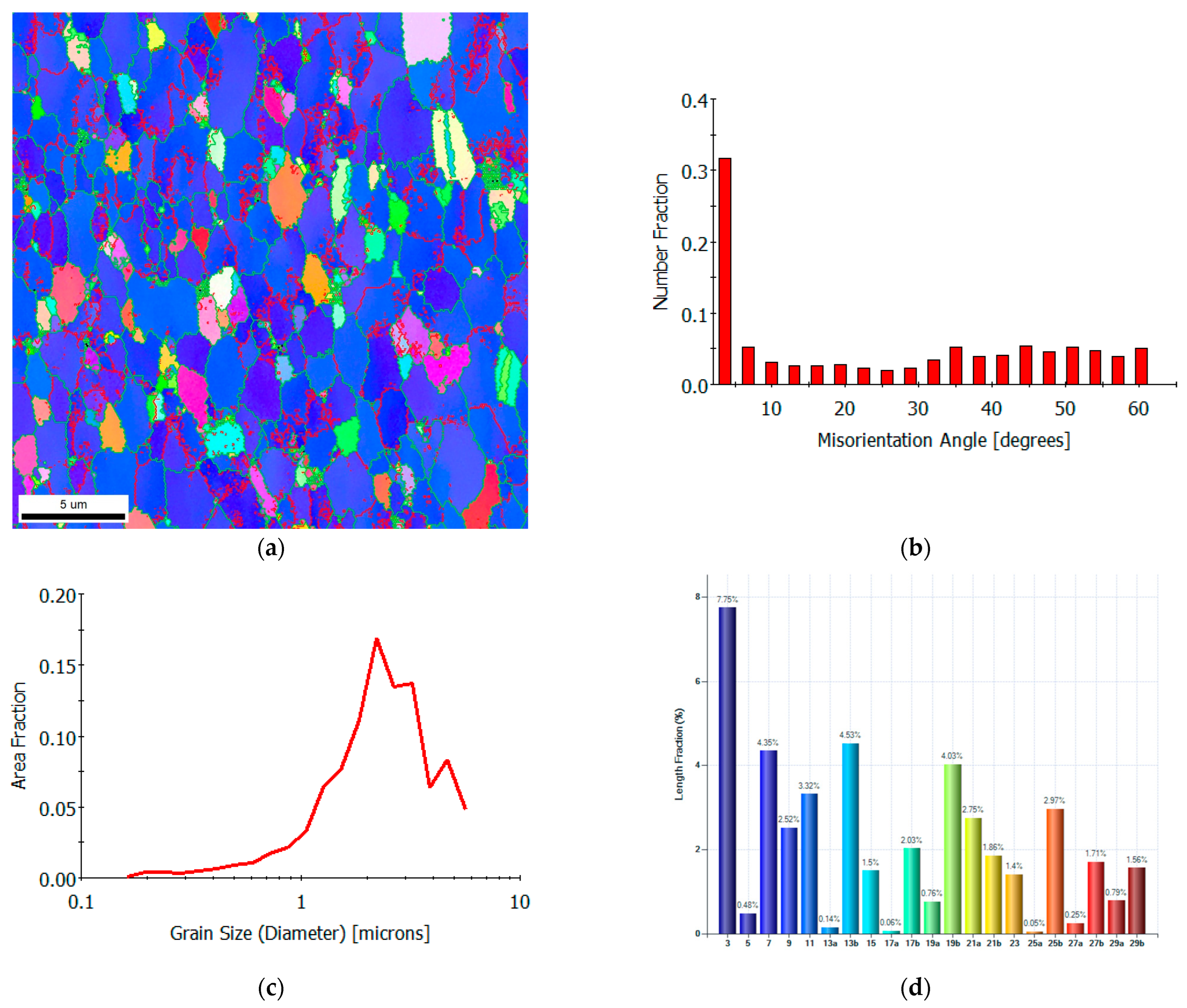
The severe plastic deformation imposed by the KOBO extrusion process profoundly refined the microstructure, as evidenced in (IPF-Z) map (Figure 1a), which shows an ultrafine-grained (UFG) microstructure with the grains exhibiting an equiaxed morphology. The analysis also revealed the development of a characteristic double fibre texture, with prominent <111> and <100> crystallographic components aligned parallel to the extrusion axis. This texture is a typical outcome for extruded FCC alloys.
A quantitative analysis of the grain boundary network (Figure 1b) indicates that low-angle grain boundaries (LAGBs, θ < 15°) account for 25.7% of the total boundary length. Within the high-angle grain boundary (HAGB) population, a prominent fraction (17%) is clustered around a 60° misorientation. This peak is characteristic of Σ3 CSL boundaries, which are typically low-energy annealing twins.
The grain size distribution histogram (Figure 1c) confirms the effective grain refinement, showing a monomodal distribution with a mean Equivalent Circle Diameter (ECD) of 0.8 µm. The grain boundary character distribution (GBCD), shown in Figure 1d, was analyzed to quantify the population of special boundaries. In the as-extruded state, the fraction of CSL boundaries is about 41%.
Following a post-KOBO extrusion annealing treatment at 500 °C for 1 h, the microstructure partially recrystallized, as detailed in the IPF map in Figure 2a. This is quantitatively confirmed by the grain size histogram (Figure 2c), which shows a minor increase in the mean ECD to about 1.2 µm. Concurrently, the initial double fibre texture was significantly weakened, tending towards a more random crystallographic orientation distribution. The annealing process also altered the grain boundary network. The histogram of grain boundary misorientation distribution shows an increase in the LAGBs fraction to about 43% (Figure 2b), with about 10% of the GBs having misorientation angles of ~60°. The persistence of a high LAGB fraction indicates that the structure has likely undergone significant recovery but has not yet fully recrystallized.
After the annealing treatment the CSL grain boundary network was modified. The GBCD histogram (Figure 2d) reveals a substantial increase in the population of low-Σ CSL boundaries. Specifically, data revealed that the fraction of low-Σ CSL boundaries increased from 41% to about 45%.
To supplement the EBSD data and resolve finer microstructural features, the grain structure on the plane perpendicular to the extrusion axis (ND-ED) was characterized using TEM.
For the as-extruded sample, TEM analysis of the transverse plane revealed a fine-grained structure with an intercept length of about 0.8 µm (Figure 3a), which agrees with the EBSD results shown above. The grains showed a tendency for elongation along the extrusion direction (ED), which is consistent with the <111> and <100> fiber texture observed in EBSD analysis and is a characteristic feature of the severe plastic deformation from the extrusion process. A key feature of this state was the presence of complex contrast features consistent with a high density of crystalline defects, primarily dislocations, which is characteristic of a highly strained material.
Following the annealing treatment, TEM analysis confirmed a transformation of the microstructure (Figure 3b). While the average grain size increased only slightly to an average intercept length of ~1.1 μm, the grains exhibited a significantly lower dislocation density, with some appearing almost dislocation-free. A key feature of the annealed state was the formation of numerous, finely dispersed precipitates approximately 10–20 nm in size (Supplementary Figure S1). The resulting microstructure is therefore best described as being in a recovered and partially recrystallized state, rather than one defined by significant grain growth.
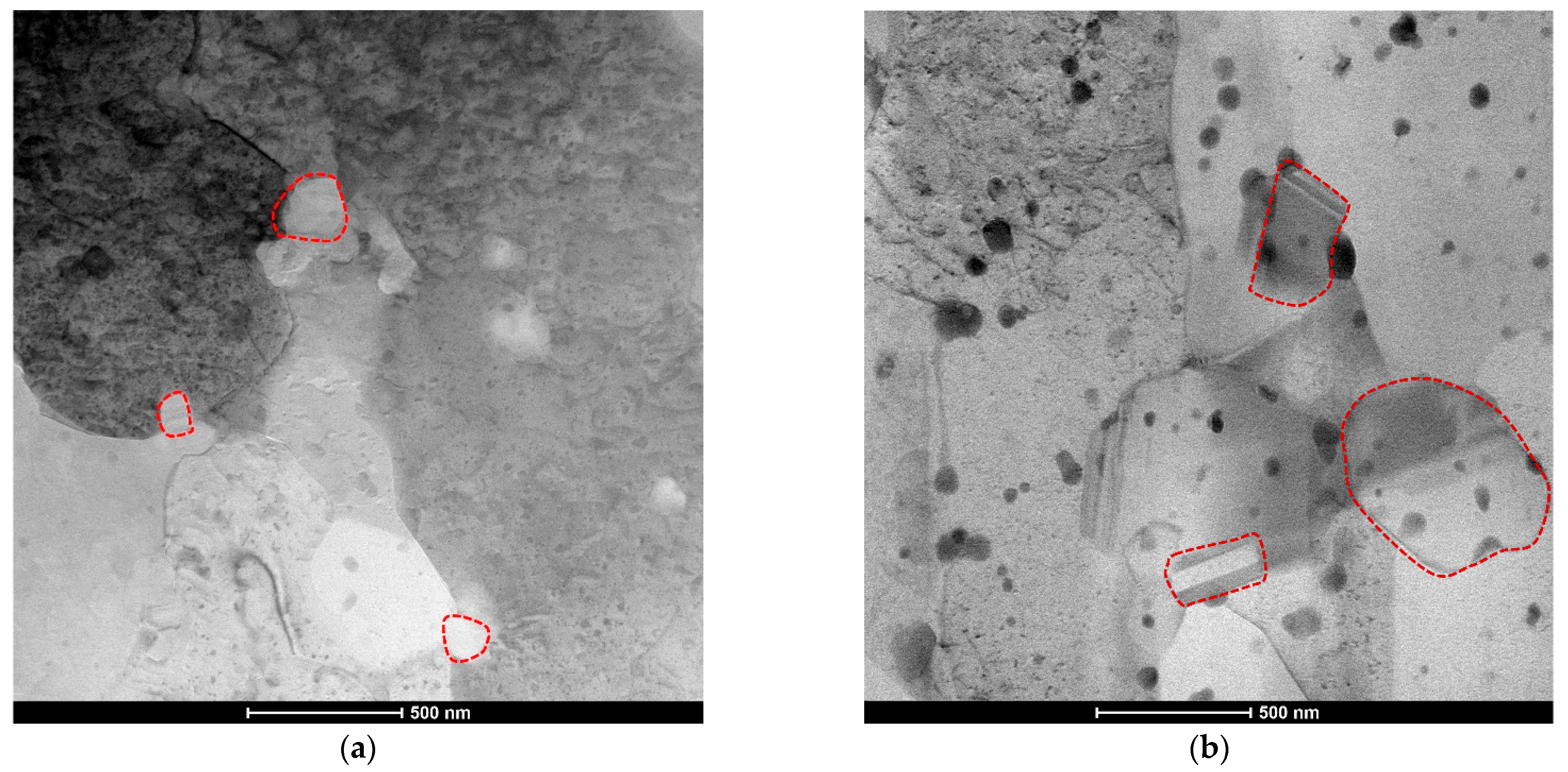
In addition to the observed changes in grain size, the annealing treatment also profoundly altered the morphology of the secondary Si phase, as illustrated in Figure 4. These features were definitively identified as Si precipitates using Selected Area Electron Diffraction (SAED), with the corresponding diffraction pattern provided in Supplementary Figure S2. This conclusion is consistent with the alloy’s nominal composition and extensive prior characterization of this material system. In the as-extruded condition, the microstructure was characterized by a high number density of homogeneously distributed, fine, spheroidal Si precipitates with sizes ranging from 110 to 150 nm (Figure 4a). Following the heat treatment at 500 °C for 1-h, significant coarsening of these particles occurred via Ostwald ripening [31], leading to a substantial increase in their size to a range of 300 to 700 nm (Figure 4b). Furthermore, a notable feature observed exclusively in the annealed state was the clear presence of annealing twins within these coarsened Si precipitates.

3.2. Effect of He Irradiation on Microstructure

Figure 5 presents low-magnification BF-TEM micrographs illustrating the irradiation-induced damage in the KOBO-processed and annealed specimens. The primary microstructural change visible at this magnification is the formation of a high density of helium bubbles in the microstructure. The location and size distribution of the helium bubbles, shown quantitatively in Figure 5c, varied significantly between the two conditions. In the KOBO-processed and annealed sample (black bars), a broad damage region is observed starting close to the surface (~25 nm). This condition is characterized by a distinct peak of large bubbles, reaching a maximum size of approximately 11.5 nm at a depth of 50 nm. The bubble size then gradually decreases at greater depths. In contrast, bubble formation in the as-processed KOBO sample (red bars) is shifted deeper into the material, beginning at a depth of about 80 nm. The bubbles in this sample are generally smaller and are concentrated in a narrower band between 80 and 200 nm, with a relatively consistent size of around 7 nm.
The TEM analysis reveals that helium bubbles exhibit a strong tendency for heterogeneous nucleation and growth along grain boundaries (indicated by yellow arrows), as shown in Figure 6. This results in a high density of bubbles decorating the boundary, which is contrasted by a distinct bubble-depleted zone within the adjacent grain matrix. This preferential segregation occurs because grain boundaries act as effective trapping sites for both helium atoms [32,33]. Furthermore, grain boundaries are preferential sinks for vacancies; due to the strong vacancy–helium binding energy, these vacancies can effectively drag helium atoms to the boundary, thereby concentrating the gas and facilitating bubble growth [34].
To characterize the irradiation-induced defects in depth, the He-irradiated samples of both the KOBO-processed and annealed materials were further investigated using STEM and HRTEM modes. The STEM-BF and STEM-HAADF image pairs for the KOBO-processed state after He+ irradiation is given in Figure 7a,b. The analysis revealed a layer of refined grains located just beneath the surface region containing helium bubbles. Within this refined microstructure, dislocation loops, with an average size of approximately 5 nm, were also observed (see yellow arrow). High-resolution TEM (HRTEM) analysis provided further details on the nature of the irradiation-induced defects (Figure 7c). The images revealed the presence of features identifiable as 1–3 atomic layer thick nanotwins (or stacking fault ribbons), as highlighted in Figure 7c. These defects appear as thin, linear features disrupting the perfect stacking sequence of the {111} planes in the FCC aluminum matrix.
A parallel investigation was conducted on the annealed sample to characterize the nano-defects induced by irradiation. The corresponding STEM-BF and STEM-HAADF images after He+ irradiation are presented in Figure 8a,b. These images reveal a high density of dislocation loops, which are characteristic of irradiation-induced damage [35,36,37]. The loops are concentrated in a layer spanning a depth of approximately 150 nm to 300 nm from the irradiated surface.
Higher magnification imaging of the annealed material reveals a strong interaction between irradiation-induced defects and the crystal lattice. A significant number of helium bubbles appear to be directly associated with the dark, linear contrast features characteristic of dislocation lines, suggesting they are either trapped at or aligned along them (Figure 8c,d). This behavior is consistent with established findings that dislocations act as preferential sinks for helium atoms and provide pathways for their rapid diffusion [38]. Additionally, the nucleation and growth of bubbles are energetically favored in the low-free-energy sites adjacent to dislocations, which results in the observed linear arrangement [39,40].

4. Discussion

The formation of helium bubbles, observed in both material conditions, originates from the implantation of He+ ions, which generates numerous point defects, including vacancies and interstitial atoms. At the elevated experimental temperature, the thermally activated diffusion of these defects and the implanted helium atoms facilitates the agglomeration of helium into vacancies. The accumulation of helium within these vacancy clusters acts to nucleate and grow the stable, high-pressure helium bubbles observed in the micrographs.
During this process, the energetic particles displace lattice atoms, creating a supersaturation of the point defects. At elevated temperatures, these defects, along with the injected helium, will inevitably agglomerate to form the bubbles, which can lead to embrittlement and material failure [41]. A primary strategy for mitigating this damage is to engineer the material’s microstructure with a high density of sinks, such as grain boundaries (GBs) and dislocations. These features act as preferential sites for trapping point defects, promoting vacancy-interstitial recombination and thereby reducing the concentration of defects available to form damaging clusters and bubbles [41,42,43]. In this article we investigated two distinct microstructural states of the same material. It was found that the grain microstructure has a profound influence on their performance under He irradiation [42,43,44].
The higher performance of the KOBO-processed material in suppressing helium bubble growth is a direct consequence of its exceptionally high and spatially homogeneous total sink strength (Stotal). As revealed, after the KOBO extrusion a microstructure characterized by ultrafine grains and a higher density of tangled dislocations was obtained, which maximize both the grain boundary (SGB ∝ d−1) and dislocation (Sd = ρd) contributions to Stotal. The dense sink network alters the kinetics of radiation-induced point defects. By providing abundant, closely spaced sites for mutual annihilation, it reduces the mean free path of vacancies and self-interstitials, thereby suppressing the vacancy supersaturation required for the nucleation of stable helium-vacancy (He-V) clusters. Consequently, helium atoms must diffuse to greater depths (~80 nm) to overcome this kinetic barrier, leading to a delayed onset of nucleation and a reduced terminal bubble size (~7 nm). Furthermore, the observation of irradiation-induced nanotwins and stacking faults is mechanistically consistent with the intense point defect fluxes interacting with the pre-existing dislocation network. Under such conditions, dislocation climb, and glide processes are accelerated, and interactions can lead to the dissociation of perfect dislocations into partials, creating stacking faults that can subsequently be arranged into twin configurations [45,46].
The heat treatment provided the thermal energy necessary to drive the microstructure towards a more stable, lower-energy state. This energy input primarily facilitated the rearrangement and annihilation of dislocations, characteristic of recovery, which significantly reduced the dislocation density. This reduction in dislocation density lowered the overall total sink strength Stotal and made the remaining sinks (grain boundaries and sparse dislocations) less competitive. This diminished capacity for point defect recombination accounts for the accelerated He-V clustering kinetics observed in the annealed sample, resulting in larger bubbles (up to 11.5 nm) forming at shallower depths (~25 nm). The cornerstone of this strategy, however, is the targeted manipulation of the grain boundary character distribution. The significant increase in the population of Σ3 twin boundaries is critical. Atomistic simulations have provided direct evidence for the unique role of these interfaces; for instance, molecular dynamics studies on Alloy 800H have shown that while high-energy, incoherent grain boundaries act as strong sinks with significant helium accumulation, coherent Σ3{111} twin boundaries show virtually no helium segregation [47]. These coherent twin boundaries (CTBs), with their low excess free volume and ordered atomic structure, are notoriously less efficient sinks for point defects [48,49]. This inefficiency displaces helium segregation away from the grain boundary plane and into the grain interior, where residual dislocations act as primary trapping sites. Concurrently, their crystallographic coherence allows them to accommodate lattice slip without generating significant stress concentrations and makes them intrinsically resistant to impurity segregation and helium-induced decohesion. This fortifies the grain boundary network against intergranular fracture, a primary failure mode in irradiated metals where He accumulation is known to degrade grain boundary strength [50,51].
Ultimately, this study elucidates a fundamental dichotomy in the design of radiation-tolerant materials. The as-extruded microstructure exemplifies a “volumetric mitigation” strategy, where a maximized sink density suppresses the accumulation of damage throughout the bulk, making it ideal for applications where swelling and volumetric stability are the primary concerns. The annealed microstructure, through Grain Boundary Engineering (GBE), employs a targeted “interfacial fortification” strategy. This approach strategically sacrifices a degree of volumetric damage resistance to specifically armor the material’s most vulnerable microstructural links—the grain boundaries—against catastrophic, fracture-driven failure. The optimal design paradigm is therefore not universal but is dictated by the anticipated primary failure mechanism and performance requirements of the specific application.

5. Conclusions

In summary, the microstructures of KOBO-extruded and KOBO-extruded and annealed samples, irradiated with He ions, were characterized using Transmission Electron Microscopy (TEM). The main conclusions are as follows:
  • Analysis by Electron Backscatter Diffraction (EBSD) showed that the KOBO-extruded sample has an average grain size of 0.8 µm and a Coincidence Site Lattice (CSL) boundary fraction of approximately 41%.
  • Following annealing, the KOBO-processed sample exhibited a larger average grain size of about 1.2 µm and a higher CSL boundary fraction of approximately 45%.
  • Helium bubbles formed in both samples because of He ion irradiation, and TEM analysis revealed that grain boundaries are preferential sites for the accumulation and growth of these bubbles.
  • The onset of helium bubble formation occurred at a greater depth in the as-extruded sample (~80 nm) compared to the annealed sample (~25 nm). The high density of defect sinks in the as-extruded material suppressed bubble nucleation near the surface, forcing helium to diffuse deeper into the material.
  • HRTEM analysis confirmed that ion irradiation induced a high density of nanoscale defects in both material conditions. In the as-extruded sample, these defects included dislocation loops and nanotwins or stacking faults, while the annealed sample showed a high density of dislocation loops.
  • The superior performance of the as-extruded sample in suppressing helium bubble growth is attributed to its high density of sinks (grain boundaries and dislocations). These sinks trapped radiation-induced point defects, promoting their annihilation and reducing the vacancy concentration required for bubble formation.

Supplementary Materials

The following supporting information can be downloaded at: https://www.mdpi.com/article/10.3390/en18205445/s1, Figure S1: (a) STEM-HAADF image in which red circle shows an area of EDS analysis, (b) results of pointwise chemical composition analysis. Figure S2. (a) TEM image of the material’s microstructure after KOBO processing and annealing at 500 °C for 1 h: (a) TEM image, and (b) its corresponding SAED pattern from the area labeled (3), indexed as the [–110] zone axis for silicon (Si).

Author Contributions

P.S.: Conceptualization, Methodology, Formal analysis, Data curation, Writing—original draft, Visualization, Project administration, Supervision. M.B.: Resources, Investigation, Writing—review & editing. J.Z.: Resources, Investigation, Writing—review & editing. M.P.: Resources, Project administration, Writing—review & editing. All authors have read and agreed to the published version of the manuscript.

Funding

The research was funded by the National Science Centre, Poland, based on the decision number 2021/43/D/ST8/01946. This paper was completed in connection with the project “Innovative and additive technologies for sustainable energy industry”, registration no. CZ.02.01.01/00/23_021/0010117 financed by the Structural Funds of European Union project.

Data Availability Statement

The original contributions presented in the study are included in the article, further inquiries can be directed to the corresponding author.

Conflicts of Interest

The authors declare no conflict of interest.

References

  1. Qiu, S.; Liu, H.; Jiang, M.; Min, S.; Gu, Y.; Wang, Q.; Yang, J.; Li, X.; Chen, Z.; Hou, J. A Brief Review on He Ion Irradiation Research of Steel and Iron-Based Alloys in Nuclear Power Plants. Acta Metall. Sin. Engl. Lett. 2023, 36, 529–551. [Google Scholar] [CrossRef]
  2. Chen, H.; Cheng, Y.; Lin, C.; Peng, J.; Liang, X.; Gao, J.; Liu, W.; Huang, H. In-Situ TEM Observation of Nanobubbles Evolution in Helium-Irradiated Aluminium upon Tensile Stressing. J. Nucl. Mater. 2019, 520, 178–184. [Google Scholar] [CrossRef]
  3. Zhu, H.; Qin, M.; Wei, T.; Davis, J.; Ionescu, M. Atomic-Scale Study of He Ion Irradiation-Induced Clustering in α-Zirconium. Acta Mater. 2023, 244, 118584. [Google Scholar] [CrossRef]
  4. Hu, Y.; Peng, L.; Shi, J.; Li, L.; Sun, Y.; Chen, S.; Wan, Y. The Temperature Effect on the Formation and Growth of Helium-Vacancy Clusters in Bcc Iron: A Comprehensive Molecular Dynamics Simulation. J. Nucl. Mater. 2024, 597, 155130. [Google Scholar] [CrossRef]
  5. Wang, J.; Liu, D.; Dang, W.; Guo, Z.; Song, W. Segregation and Coalescence Behavior of Helium Bubbles in Tungsten. J. Nucl. Mater. 2021, 544, 152732. [Google Scholar] [CrossRef]
  6. Yoshida, N.; Iwakiri, H.; Tokunaga, K.; Baba, T. Impact of Low Energy Helium Irradiation on Plasma Facing Metals. J. Nucl. Mater. 2005, 337–339, 946–950. [Google Scholar] [CrossRef]
  7. Li, J.-T.; Beyerlein, I.J.; Han, W.-Z. Helium Irradiation-Induced Ultrahigh Hardening in Niobium. Acta Mater. 2022, 226, 117656. [Google Scholar] [CrossRef]
  8. Kishimoto, H.; Yutani, K.; Kasada, R.; Kimura, A. Helium Cavity Formation Research on Oxide Dispersed Strengthening (ODS) Ferritic Steels Utilizing Dual-Ion Irradiation Facility. Fusion Eng. Des. 2006, 81, 1045–1049. [Google Scholar] [CrossRef]
  9. Shang, Z.; Niu, T.; Sun, T.; Xue, S.; Fan, C.; Chen, W.-Y.; Li, M.; Wang, H.; Zhang, X. In Situ Study on Radiation Response of a Nanotwinned Steel. Scr. Mater. 2022, 220, 114920. [Google Scholar] [CrossRef]
  10. Wang, L.; Yan, S.; Meng, M.; Xue, K.; Li, P. Twin Boundary-Assisted Improvement of Radiation Resistance of Iron: Defect Evolution, Mechanical Properties, and Deformation Mechanism. J. Nucl. Mater. 2022, 567, 153818. [Google Scholar] [CrossRef]
  11. Cao, P.; So, K.P.; Yang, Y.; Park, J.G.; Li, M.; Yan, L.; Hu, J.; Kirk, M.; Li, M.; Lee, Y.H.; et al. Carbon Nanotube (CNT) Metal Composites Exhibit Greatly Reduced Radiation Damage. Acta Mater. 2021, 203, 116483. [Google Scholar] [CrossRef]
  12. Bhattacharya, A.; Zinkle, S.J.; Henry, J.; Levine, S.M.; Edmondson, P.D.; Gilbert, M.R.; Tanigawa, H.; Kessel, C.E. Irradiation Damage Concurrent Challenges with RAFM and ODS Steels for Fusion Reactor First-Wall/Blanket: A Review. J. Phys. Energy 2022, 4, 034003. [Google Scholar] [CrossRef]
  13. Wu, Z.F.; Xu, L.D.; Chen, H.Q.; Liang, Y.X.; Du, J.L.; Wang, Y.F.; Zhang, S.L.; Cai, X.C.; Sun, B.R.; Zhang, J.; et al. Significant Suppression of Void Swelling and Irradiation Hardening in a Nanograined/Nanoprecipitated 14YWT-ODS Steel Irradiated by Helium Ions. J. Nucl. Mater. 2022, 559, 153418. [Google Scholar] [CrossRef]
  14. Xie, Z.; Guo, L.; Chen, Y.; Long, Y.; Lv, P.; Li, F.; Luo, H.; Lin, W.; Yin, Z.; Cao, J.; et al. Deterioration of Irradiation Resistance of ODS-F/M Steel under High Concentration of Helium. J. Nucl. Mater. 2023, 577, 154293. [Google Scholar] [CrossRef]
  15. Barr, C.M.; El-Atwani, O.; Kaoumi, D.; Hattar, K. Interplay Between Grain Boundaries and Radiation Damage. JOM 2019, 71, 1233–1244. [Google Scholar] [CrossRef]
  16. El-Atwani, O.; Nathaniel, J.E.; Leff, A.C.; Muntifering, B.R.; Baldwin, J.K.; Hattar, K.; Taheri, M.L. The Role of Grain Size in He Bubble Formation: Implications for Swelling Resistance. J. Nucl. Mater. 2017, 484, 236–244. [Google Scholar] [CrossRef]
  17. Nathaniel, J.E.; El-Atwani, O.; Huang, S.; Marian, J.; Leff, A.C.; Baldwin, J.K.; Hattar, K.; Taheri, M.L. Implications of Microstructure in Helium-Implanted Nanocrystalline Metals. Materials 2022, 15, 4092. [Google Scholar] [CrossRef]
  18. Saeed, A.; Mohamed, R.H.; Abu-Raia, W.A. Nickel-Free Austenitic Stainless Steel Alloys as a Sodium-Cooled Fast Reactor Fuel Cladding. Mater. High Temp. 2022, 39, 380–386. [Google Scholar] [CrossRef]
  19. Cheng, G.M.; Xu, W.Z.; Wang, Y.Q.; Misra, A.; Zhu, Y.T. Grain Size Effect on Radiation Tolerance of Nanocrystalline Mo. Scr. Mater. 2016, 123, 90–94. [Google Scholar] [CrossRef]
  20. Chen, Y.; Yu, K.Y.; Liu, Y.; Shao, S.; Wang, H.; Kirk, M.A.; Wang, J.; Zhang, X. Damage-Tolerant Nanotwinned Metals with Nanovoids under Radiation Environments. Nat. Commun. 2015, 6, 7036. [Google Scholar] [CrossRef]
  21. Manna, M.; Pal, S. Molecular Dynamics Simulation for Radiation Response of Nb Bicrystal Having Σ 13, Σ 29, and Σ 85 Grain Boundary. J. Appl. Phys. 2023, 133, 165902. [Google Scholar] [CrossRef]
  22. Manna, M.; Pal, S. Improvement in Radiation Resistance of Nanocrystalline Cu Using Grain Boundary Engineering: An Atomistic Simulation Study. J. Mater. Sci. 2022, 57, 19832–19845. [Google Scholar] [CrossRef]
  23. Han, W.Z.; Demkowicz, M.J.; Fu, E.G.; Wang, Y.Q.; Misra, A. Effect of Grain Boundary Character on Sink Efficiency. Acta Mater. 2012, 60, 6341–6351. [Google Scholar] [CrossRef]
  24. Snopiński, P.; Matus, K. Characterisation of Microstructure and Special Grain Boundaries in LPBF AlSi10Mg Alloy Subjected to the KoBo Extrusion Process. Symmetry 2023, 15, 1634. [Google Scholar] [CrossRef]
  25. Snopiński, P.; Liverić, L.; Beniak, J. Annealing Effects on Microstructure and Texture in KOBO-Processed LPBF AlSi10Mg Alloy: Elucidating CSL Boundary Formation. Symmetry 2024, 16, 1663. [Google Scholar] [CrossRef]
  26. Snopiński, P. Effects of KoBo-Processing and Subsequent Annealing Treatment on Grain Boundary Network and Texture Development in Laser Powder Bed Fusion (LPBF) AlSi10Mg Alloy. Symmetry 2024, 16, 122. [Google Scholar] [CrossRef]
  27. Bochniak, W.; Ostachowski, P.; Korbel, A.; Łagoda, M. Potential of the KOBO Extrusion Process for Nonferrous Metals in the Form of Solids and Chips. Int. J. Adv. Manuf. Technol. 2023, 127, 733–750. [Google Scholar] [CrossRef]
  28. Bochniak, W.; Marszowski, K.; Korbel, A. Theoretical and Practical Aspects of the Production of Thin-Walled Tubes by the KOBO Method. J. Mater. Process. Technol. 2005, 169, 44–53. [Google Scholar] [CrossRef]
  29. Korbel, A.; Bochniak, W.; Ostachowski, P.; Błaż, L. Visco-Plastic Flow of Metal in Dynamic Conditions of Complex Strain Scheme. Metall. Mater. Trans. A 2011, 42, 2881–2897. [Google Scholar] [CrossRef]
  30. Bochniak, W.; Korbel, A.; Ostachowski, P.; Łagoda, M. Plastic Flow of Metals under Cyclic Change of Deformation Path Conditions. Arch. Civ. Mech. Eng. 2018, 18, 679–686. [Google Scholar] [CrossRef]
  31. Alghamdi, F.; Song, X.; Hadadzadeh, A.; Shalchi-Amirkhiz, B.; Mohammadi, M.; Haghshenas, M. Post Heat Treatment of Additive Manufactured AlSi10Mg: On Silicon Morphology, Texture and Small-Scale Properties. Mater. Sci. Eng. A 2020, 783, 139296. [Google Scholar] [CrossRef]
  32. Wang, Y.; Meng, J.; Jia, F.; Cao, F.; Jiang, Y. Effects of Helium and Vacancy in Ni Symmetric Tilt Grain Boundaries by First-Principles. Nucl. Mater. Energy 2024, 40, 101721. [Google Scholar] [CrossRef]
  33. Zhang, X.; Yang, L.; Zhang, Y.; Zhang, P.; Huang, X.; Huang, S.; Hu, K.; Tang, J.; Deng, L.; Deng, H.; et al. First-Principles Study of the Trapping Behavior of Hydrogen Atoms by Defects in Vanadium Alloys. Int. J. Hydrogen Energy 2025, 128, 425–431. [Google Scholar] [CrossRef]
  34. Uberuaga, B.P.; Vernon, L.J.; Martinez, E.; Voter, A.F. The Relationship between Grain Boundary Structure, Defect Mobility and Grain Boundary Sink Efficiency. Sci. Rep. 2015, 5, 9095. [Google Scholar] [CrossRef]
  35. Zhang, W.; Chen, Y.; Cheng, W.; Guo, L.; Jin, S. Study on the Mechanism of He Effect on Dislocation Loop Formation in Three Types of Dual Ion Beam Irradiations. J. Nucl. Mater. 2024, 588, 154782. [Google Scholar] [CrossRef]
  36. Zhang, J.; Wu, Z.; Huang, J.; Li, J.; Wei, H.; Zhang, T.; Polcar, T.; Daghbouj, N.; Li, B. Damage Behavior of He-Irradiated Sintered SiC at High Temperatures. J. Nucl. Mater. 2025, 612, 155839. [Google Scholar] [CrossRef]
  37. Li, N.; Fu, E.G.; Wang, H.; Carter, J.J.; Shao, L.; Maloy, S.A.; Misra, A.; Zhang, X. He Ion Irradiation Damage in Fe/W Nanolayer Films. J. Nucl. Mater. 2009, 389, 233–238. [Google Scholar] [CrossRef]
  38. Edwards, D.J.; Schemer-Kohrn, A.; Olszta, M.; Prabhakaran, R.; Zhu, Y.; Wang, J.; Haag, J.; El Atwani, O.; Lach, T.G.; Toloczko, M. Understanding and Removing FIB Artifacts in Metallic TEM Samples Using Flash Electropolishing. J. Nucl. Mater. 2025, 606, 155618. [Google Scholar] [CrossRef]
  39. Kohnert, A.A.; Capolungo, L. A Novel Approach to Quantifying the Kinetics of Point Defect Absorption at Dislocations. J. Mech. Phys. Solids 2019, 122, 98–115. [Google Scholar] [CrossRef]
  40. Edmondson, P.D.; Parish, C.M.; Zhang, Y.; Hallén, A.; Miller, M.K. Helium Entrapment in a Nanostructured Ferritic Alloy. Scr. Mater. 2011, 65, 731–734. [Google Scholar] [CrossRef]
  41. Wurmshuber, M.; Frazer, D.; Balooch, M.; Issa, I.; Bachmaier, A.; Hosemann, P.; Kiener, D. The Effect of Grain Size on Bubble Formation and Evolution in Helium-Irradiated Cu-Fe-Ag. Mater. Charact. 2021, 171, 110822. [Google Scholar] [CrossRef]
  42. Nathaniel, J.E.; Suri, P.K.; Hopkins, E.M.; Wen, J.; Baldo, P.; Kirk, M.; Taheri, M.L. Grain Boundary Strain as a Determinant of Localized Sink Efficiency. Acta Mater. 2022, 226, 117624. [Google Scholar] [CrossRef]
  43. Zhang, Y.; Jiang, W.Q.; Gokhman, A.; Yang, J.J.; Shi, K.; Luan, J.H.; Cui, Y.; Liaw, P.K.; Liu, C.T.; Zhang, Z.W. Enhanced Irradiation Tolerance of Fe30Cr25Ni20Co15Mn10 High-Entropy Alloy via Nanotwin Boundaries. J. Nucl. Mater. 2021, 557, 153292. [Google Scholar] [CrossRef]
  44. Bian, Y.-N.; Lu, Y.; Zhang, J.; Gao, B.; Wang, W.-B.; Han, W.-Z. Interaction of Irradiation Defects with Precipitates in CuCrZr and Cu-1Fe Alloys. Acta Mater. 2023, 253, 118964. [Google Scholar] [CrossRef]
  45. Chai, J.; Zhu, D.; Guo, Z.; Wang, B.; Yan, R.; Ding, R.; Li, C.; Gao, B.; Xuan, C.; Wang, Z.; et al. Microstructure Evolution and Hardening of Helium Ion Irradiated Tungsten. Vacuum 2025, 235, 114153. [Google Scholar] [CrossRef]
  46. Fan, Y. Atomistic Modeling of Microstructural Defect Evolution in Alloys Under Irradiation: A Comprehensive Review. Appl. Sci. 2025, 15, 9110. [Google Scholar] [CrossRef]
  47. Cheik Njifon, I.; Torres, E. Effect of Grain Boundaries on the Helium Degradation Mechanisms of Alloy 800H: A Molecular Dynamics Study. J. Nucl. Mater. 2025, 603, 155395. [Google Scholar] [CrossRef]
  48. Li, B.; Li, H.-Y.; Luo, S.-N. Molecular Dynamics Simulations of Displacement Cascades in Nanotwinned Cu. Comput. Mater. Sci. 2018, 152, 38–42. [Google Scholar] [CrossRef]
  49. Zhang, L. Understanding the Radiation Resistance Mechanisms of Nanocrystalline Metals from Atomistic Simulation. Metals 2021, 11, 1875. [Google Scholar] [CrossRef]
  50. Yao, X.; Wen, M.; Xiong, K.; Mao, Y.; Guo, Y.-F. Effect of Elemental Segregation on Grain Boundary Cohesion in Platinum: A First-Principles Study. Philos. Mag. 2025, 105, 895–918. [Google Scholar] [CrossRef]
  51. Zhang, L.; Fu, C.-C.; Hayward, E.; Lu, G.-H. Properties of He Clustering in α-Fe Grain Boundaries. J. Nucl. Mater. 2015, 459, 247–258. [Google Scholar] [CrossRef]
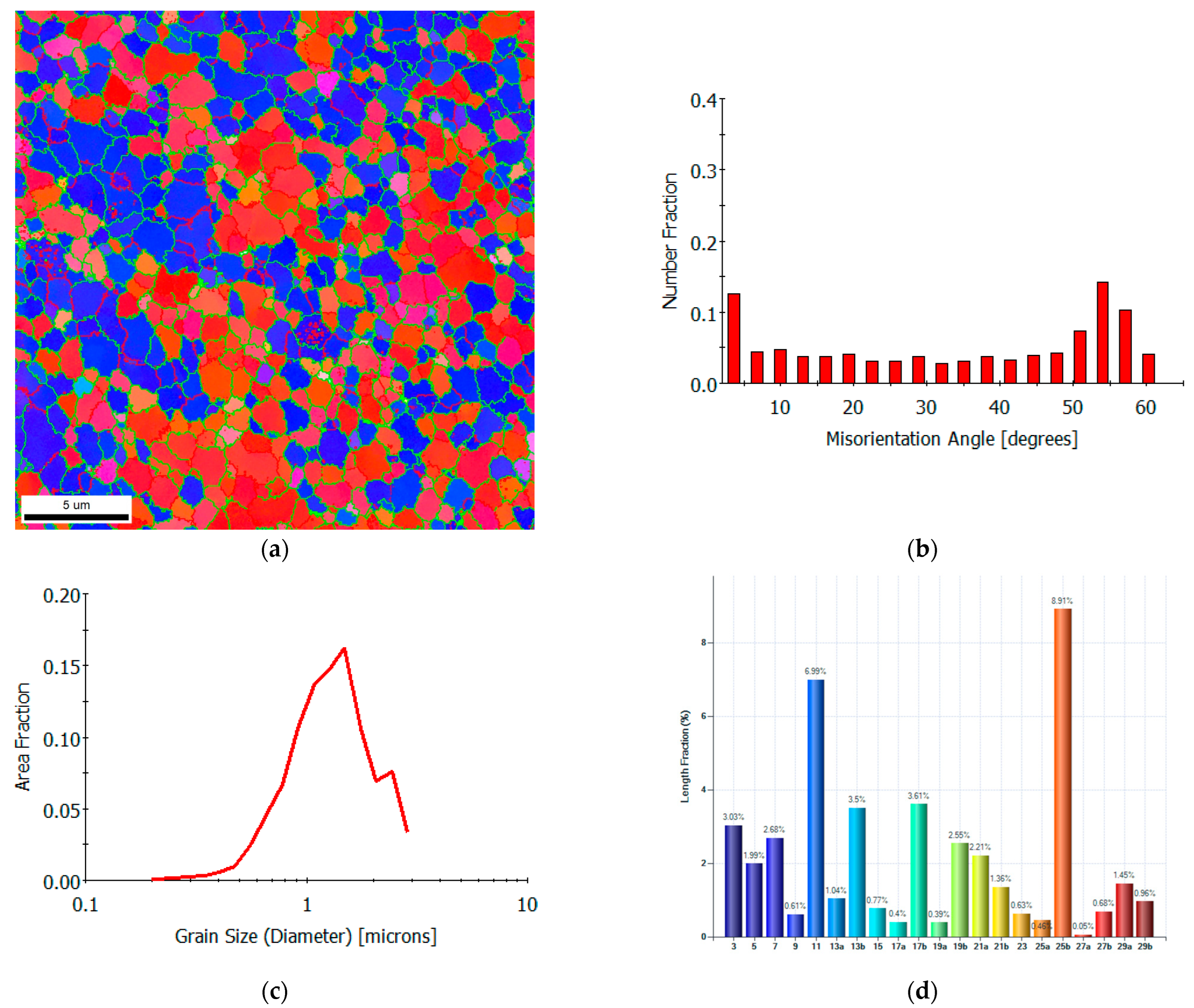
Figure 1. Microstructural characterization of the KOBO-processed LPBF AlSi10Mg alloy via Electron Backscatter Diffraction (EBSD). The figure shows (a) an Inverse Pole Figure (IPF-Z) map of the grain structure. In this map red lines correspond to LAGBs while green lines correspond to HAGBs. The scale bar shows a 5-micrometer-long line, (b) the distribution of grain boundary misorientation angles, (c) the corresponding grain size distribution, and (d) the relative fractions of different CSL grain boundary types.
Energies 18 05445 g001
Figure 2. Microstructural characterization of the KOBO-processed LPBF AlSi10Mg alloy via Electron Backscatter Diffraction (EBSD). The figure shows (a) an Inverse Pole Figure (IPF-Z) map of the grain structure. In this map red lines correspond to LAGBs and green lines to HAGBs. The scale bar shows a 5-micrometer-long line, (b) the distribution of grain boundary misorientation angles, (c) the corresponding grain size distribution, and (d) the relative fractions of different CSL grain boundary types. Note that in (a) some grains appear slightly elongated, this is likely a measurement artifact caused by sample drift during the EBSD scan and not a true representation of the grain morphology.
Energies 18 05445 g002
Figure 3. Low-magnification STEM micrographs of the grain structure on the transverse (ND-ED) plane: (a) KOBO-processed condition, and (b) KOBO-processed and annealed at 500 °C for 1 h. The extrusion direction (ED) aligns with the shorter side of the image.
Energies 18 05445 g003
Figure 4. STEM images revealing the Si precipitate evolution in the KOBO-processed LPBF AlSi10Mg alloy before and after heat treatment. (a) Micrograph of the as-extruded sample, revealing a high density of fine Si particles. (b) Micrograph of the sample after annealing at 500 °C for 1 h, showing substantial particle growth and coarsening. The Si precipitates in the images are outlined with red dashed lines for clarity.
Energies 18 05445 g004
Figure 5. Low-magnification BF-TEM images of irradiation damage in (a) KOBO-processed LPBF AlSi10Mg alloy sample, (b) KOBO-processed and annealed AlSi10Mg alloy sample, (c) He bubble size distribution in both samples.
Energies 18 05445 g005
Figure 6. High-magnification TEM micrograph showing the preferential formation of helium bubbles on grain boundaries. Under these imaging conditions, the low-density bubbles appear with bright contrast. Yellow arrows indicate large He bubbles formed along the grain boundaries.
Energies 18 05445 g006
Figure 7. TEM analysis of irradiation-induced defects in the KOBO-processed AlSi10Mg alloy: (a) STEM-BF micrograph, (b) the corresponding STEM-HAADF micrograph, (c) HRTEM image showing stacking faults (as indicated by white arrows).
Energies 18 05445 g007
Figure 8. TEM analysis of irradiation-induced defects in the KOBO-processed and annealed AlSi10Mg alloy: (a) STEM-BF micrograph, (b) the corresponding STEM-HAADF micrograph, (c) higher magnification STEM-BF micrograph revealing a highly dislocated area (yellow arrows), (d) the corresponding STEM-HAADF micrograph. Note that blue lines separate area where larger He bubbles are trapped/aligned along dislocations. In the STEM-HAADF image (d), contrast is sensitive to atomic number; thus, the low-density He bubbles appear as dark regions, while the matrix appears brighter. Note that blue lines separate areas where larger He bubbles are trapped/aligned along dislocations.
Energies 18 05445 g008
Disclaimer/Publisher’s Note: The statements, opinions and data contained in all publications are solely those of the individual author(s) and contributor(s) and not of MDPI and/or the editor(s). MDPI and/or the editor(s) disclaim responsibility for any injury to people or property resulting from any ideas, methods, instructions or products referred to in the content.