1. Introduction
The conversion of solar energy via photovoltaic (PV) devices offers a compelling pathway to sustainable electricity generation, owing to high power yields, long-term operational stability, minimal user intervention, and versatile installation options on rooftops and façades. Coupled with rapidly declining levelized costs, PV has emerged as a cornerstone of Europe’s clean energy transition. By the end of 2024, the EU surpassed its REPowerEU target—installing approximately 339.4 GW of solar capacity, up from 320 GW—and is on course to achieve 600 GW by 2030, driven by record annual additions of 62.5 GW in 2024, projected to be 70 GW in 2025. Solar power overtook coal in 2024, supplying over 11% of EU electricity, with Central and Eastern European markets such as Poland increasing their capacity from 9 GW in 2019 to 46 GW in 2024 despite regulatory and financial hurdles [
1].
Silicon remains the dominant PV technology, accounting for roughly 95% of the global market. Its combination of earth abundance, non-toxicity, and mature manufacturing has led to a record single-junction efficiency of 27.3% (NREL, June 2025) and driven costs downward. However, the theoretical Shockley–Queisser limit for silicon (≈29.4%) has nearly been reached, prompting interest in tandem architectures. Over the past decade, organic–inorganic perovskites have emerged as an ideal high-bandgap top cell material, enabling monolithic silicon/perovskite tandems with demonstrated efficiencies up to 34.9% [
2]. By stacking absorbers with complementary bandgaps, tandem cells reduce thermalization losses in the top junction and harvest sub-bandgap photons in the silicon bottom cell, pushing the thermodynamic efficiency limit toward 43% [
3,
4]. This spectral splitting approach represents a promising strategy for surpassing the intrinsic efficiency ceiling of single-junction devices [
5].
Silicon nanowire texturization is well established as an effective surface engineering strategy in photovoltaics, reducing front-surface reflectance and thereby increasing photon absorption within the silicon substrate. By transforming the Si surface from a smooth to a high-aspect-ratio, roughened morphology, nanowire arrays enable enhanced light trapping and improved photovoltaic efficiency [
6,
7]. Surface texturization via metal-assisted etching (MAE) is highly effective for creating “black silicon” with dramatically reduced reflectivity and near-total solar absorption. Based on extensive experience with the texture of MAE-fabricated nanowire structures, the authors are now investigating vertically aligned silicon nanowires as a scaffold for subsequent functional layers in tandem solar cells. In particular, these high-aspect-ratio textures offer an ideal platform for the conformal deposition of transparent conductive oxides as recombination layers, as well as perovskite absorbers, enabling novel tandem architectures that remain largely unexplored in the current literature [
8]. However, literature reports indicate that depositing perovskite onto textured silicon can significantly benefit tandem cell performance by minimizing front-surface reflectance and maximizing photocurrent. To date, most studies have focused on classic pyramidal texturing, where perovskite films conformally coated pyramidal facets to achieve low optical losses and photocurrents exceeding 20 mA cm
−2 in each subcell [
3]. The benefits of pyramidal fully textured tandems have been demonstrated [
9,
10,
11]. However, conformal perovskite deposition on pyramidal textures requires complex, high-cost techniques that have yet to see widespread industrial adoption, owing to the challenge of uniformly filling pyramidal valleys without material buildup. Wet chemical deposition methods offer a lower-cost alternative but demand a porous scaffold to support uniform perovskite infiltration. Common scaffolds for perovskite cells employ porous Al
2O
3 or TiO
2 matrices [
12,
13]; for example, TiO
2 nanowire arrays (~300 nm tall) have enabled stable perovskite infiltration and enhanced device efficiency [
14]. Building on our experience in producing silicon nanowires of comparable dimensions (~300–400 nm height), we explore their use as an innovative porous scaffold for perovskite deposition in tandem solar architectures.
Silicon/perovskite tandem cells represent a promising and innovative direction for next-generation photovoltaics, where two key factors govern the effective interconnection of a tandem cell. Firstly, their architecture necessitates a transparent conductive oxide (TCO) interlayer to provide efficient electrical coupling between the silicon and perovskite subcells to form a monolithic two-terminal (2T) tandem configuration [
15], and secondly, the precise current matching between the silicon and perovskite subcells is essential to avoid power losses [
5,
16,
17,
18]. The subcells are interconnected by a single recombination layer, requiring only two external contacts—one of which must be semitransparent to allow for light transmission to the bottom junction [
19]. This recombination interface must combine low electrical resistance with minimal optical absorption to enable efficient hole–electron recombination between subcells [
20,
21,
22,
23,
24,
25,
26]. Moreover, the deposition of the perovskite top cell must not compromise the light harvesting or electrical performance of the textured silicon bottom cell, which further challenges the integration of uniform, high-quality layers on rough, high-aspect-ratio surfaces [
4]. Building on our expertise in silicon nanowire texturization and the demonstrated benefits of high-aspect-ratio scaffolds for tandem photovoltaics, we have extended this work to the deposition of recombination layers directly onto SiNW arrays. To date, we have deposited both indium–tin oxide (ITO) and tin dioxide (SnO
2) films as interconnecting layers, demonstrating proof of concept for conformal, low-loss contacts in monolithic silicon/perovskite tandem architectures [
15,
27]. In the paper, the authors extend this approach by implementing aluminum-doped zinc oxide (AZO) films in the same recombination layer role.
The selection of an appropriate recombination layer material is critical, with aluminum-doped zinc oxide (AZO) emerging as an excellent candidate among various transparent conductive oxides [
28,
29]. As a viable ITO alternative, AZO combines long-term stability with high electrical conductivity and visible-range transparency, making it suitable for applications ranging from touch screens and LEDs to organic photovoltaic devices [
30,
31,
32,
33,
34,
35]. To function effectively as a transparent electrode, TCO films must exhibit low resistivity (≤10
−3 Ω·cm) and maintain optical transmittance above 80% at thicknesses below 200 nm while also offering robust mechanical durability and strong substrate adhesion. Magnetron sputtering, a scalable and versatile thin-film deposition technique frequently employed in industry, meets these requirements and supports precise control over film properties [
36].
For the deposition of AZO thin films by magnetron sputtering, the most commonly used targets are made of sintered zinc oxide powders and aluminum oxide (ZnO-Al
2O
3). The optimal percentage of aluminum oxide in such targets is approximately 2% [
37,
38,
39,
40,
41,
42,
43,
44,
45,
46,
47,
48,
49]. Studies aiming to minimize AZO resistivity have typically adjusted the Al
2O
3 fraction within the sputtering target to between 1 and 6 mol% [
39,
40,
43]. The reactive sputtering of a Zn–Al metal target in an Ar/O
2 atmosphere has likewise produced low-resistivity films [
39,
41,
43,
44,
45,
50,
51,
52], and co-sputtering from separate ZnO and Al targets has enabled the fine tuning of composition via independent power control [
41,
51,
52]. In these processes, the target power densities are generally a few W cm
−2, and substrates are often maintained at elevated temperatures (~500 °C) to promote film crystallinity. Under such conditions, film resistivities as low as 1 × 10
−4 to 1 × 10
−3 Ω cm have been reported, alongside visible-range transmittances exceeding 80%. Post-deposition annealing further reduces resistivity and enhances optical transparency.
Beyond magnetron sputtering, a variety of deposition methods—such as pulsed laser deposition, chemical vapor deposition, sol–gel techniques, and atomic layer deposition (ALD)—have been employed to fabricate transparent conductive films. Among these, ALD has gained significant attention for its ability to produce exceptionally uniform coatings at a low cost and low processing temperatures, even on substrates with complex geometries. While pulsed laser deposition can yield films with superior electrical properties, its scalability to industrial scales is limited. Magnetron sputtering remains a practical option for high-throughput production, but ALD stands out for its sub-nanometer thickness control, large-area compatibility, and conformal coverage capabilities [
53], making it particularly well suited to textured or high-aspect-ratio surfaces. In ALD, alternating exposures to precursor and reactant gases allow for the sequential formation of single molecular layers, enabling precise thickness and composition control via self-limiting surface reactions [
54]. This approach has been successfully used to deposit uniform coatings on nanowire arrays and other nanostructures [
55,
56,
57]. Although several methods have been applied to synthesize transparent Al-doped ZnO films, achieving uniform dopant distribution and stable electrical behavior remains challenging. ALD’s inherent precision in precursor dosing and exposure timing offers a promising route to high-quality AZO films, yet studies on ALD-grown AZO remain relatively scarce [
58,
59,
60].
We report for the first time the integration of an AZO layer in function of a recombination layer on high-aspect-ratio silicon nanowire (SiNW) scaffolds, addressing the critical challenge of conformal coverage on porous, vertically aligned arrays. By comparing AZO films deposited by magnetron sputtering and ALD methods on identical SiNW templates via SEM, TEM, optical transmission, and electrical measurements, we delineate how deposition mechanism and film thickness jointly influence conformality, microstructure, and optoelectronic performance, thereby establishing process guidelines for AZO-based recombination interfaces in next-generation tandem photovoltaics.
3. Results
3.1. SEM Analysis of AZO Thin Films on Silicon Nanowire Substrates
The morphological quality and coverage uniformity of AZO layers deposited on silicon nanowire (SiNW) scaffolds play a critical role in determining the overall electrical and optical performance of tandem solar cell architectures. Given the high aspect ratio and porous nature of vertically aligned SiNWs, achieving conformal and continuous AZO coatings presents significant challenges that are highly dependent on the selected deposition method.
To assess the surface topography, film continuity, and penetration depth of the AZO layers within the nanowire matrix, scanning electron microscopy (SEM) was employed. High-resolution SEM imaging enables the direct visualization of the layer morphology on both the cross-sectional profiles of the nanostructured substrate. By comparing coatings obtained via atomic layer deposition and magnetron sputtering, key differences in coverage quality, thickness uniformity, and structural integrity can be elucidated.
Such imaging-based analysis provides critical insights into the interaction between deposition parameters and complex substrate geometry, guiding the optimization of AZO films for enhanced charge transport, light management, and interfacial properties in nanostructured tandem photovoltaic devices.
3.1.1. AZO Layer Deposited Using ALD Method
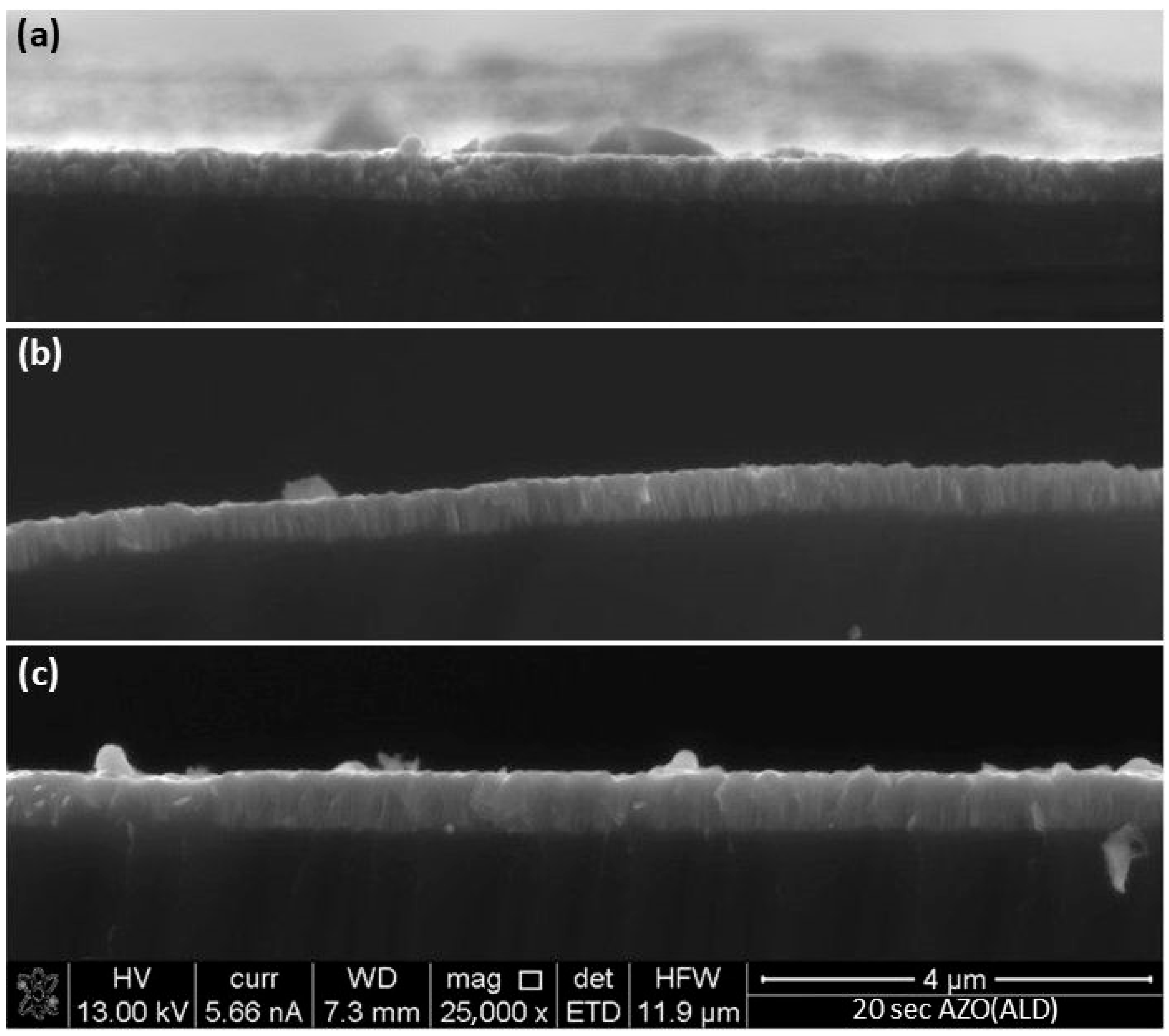
Figure 1a presents a cross-sectional view of an AZO layer deposited onto vertically aligned silicon nanowires, imaged at a magnification of 25,000×. Deposition was conducted after 20 s of silicon nanowire etching (estimated nanowire length ~300–500 nm). The AZO film appears as a bright, conformal layer covering the top surface of the porous scaffold and interwire area. Some surface roughness and agglomerates are visible in the uppermost part of the layer, likely resulting from non-uniform film nucleation or partial densification during growth. Despite the challenging high-aspect-ratio morphology, the coverage suggests effective material penetration, characteristic of a well-optimized atomic layer deposition (ALD) process. No apparent voids or delamination zones are observed between the AZO and the SiNW base layer, indicating good interfacial adhesion.
This SEM cross-section in
Figure 1b shows silicon nanowires (~300–500 nm long) coated with a thicker AZO film compared to the AZO(ALD)-1 sample. The brighter, continuous AZO layer exhibits improved thickness uniformity and complete top-surface coverage, extending deeper into the porous scaffold. The increased film thickness is caused by a higher number of ALD cycles. The conformal nature of the coating is well preserved despite the higher layer volume, confirming that the ALD process maintains its self-limiting growth behavior and effective precursor infiltration even at advanced deposition stages. No apparent cracks or delamination are visible, which is critical for the structural integrity and optoelectronic performance of nanowire-based tandem solar cells.
Figure 1c shows an AZO layer of increased thickness compared to previous samples. The film remains conformal and continuous along the nanowire scaffold, confirming the trend of uniform layer growth with increasing deposition time. This behavior is consistent with the self-limiting mechanism of the ALD process on high-aspect-ratio structures.
However, there are specific locations in the sample where the AZO overgrowth dramatically alters the nanowire topology; one of these is shown in
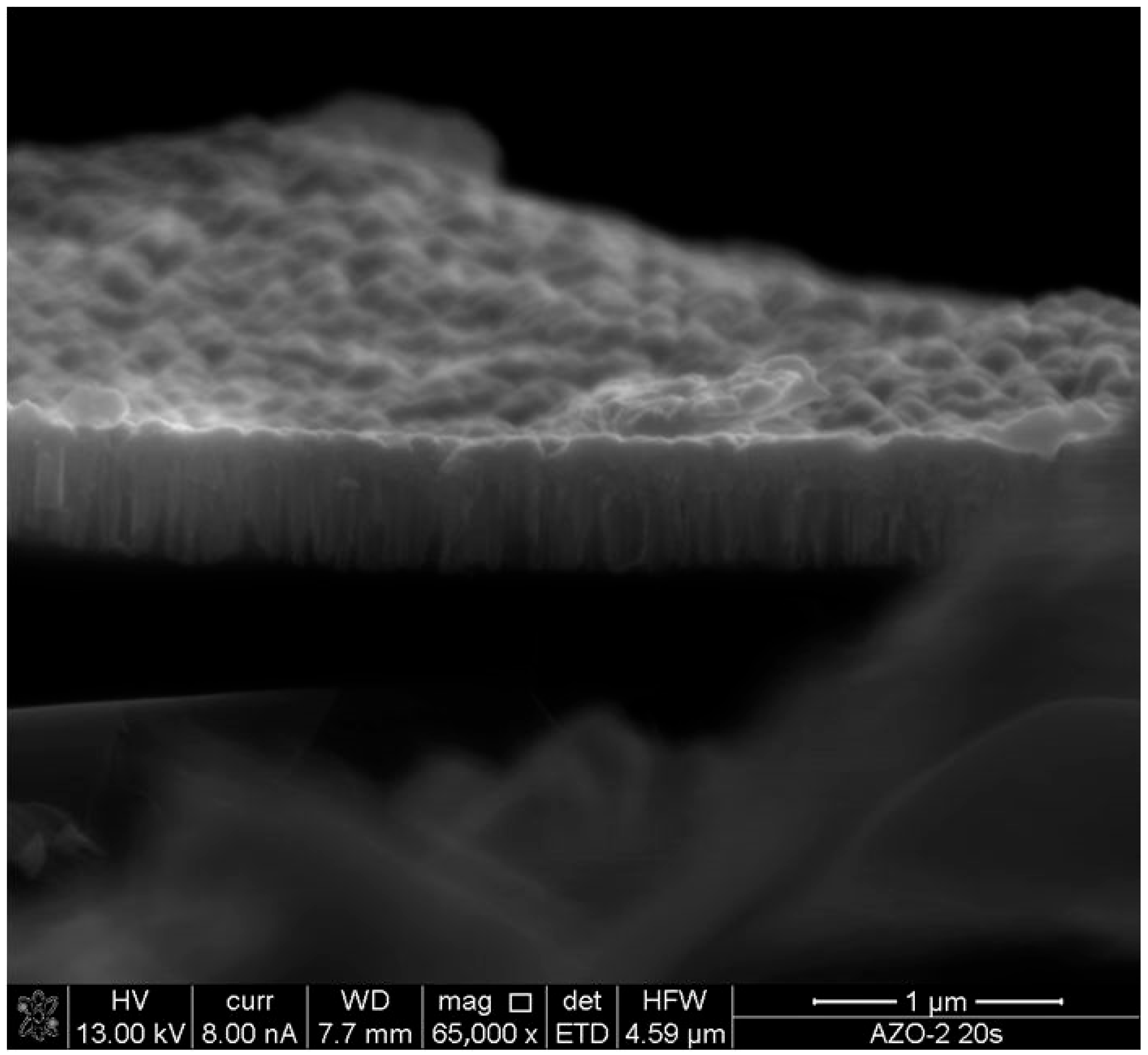
Figure 2. Here, the ALD-deposited AZO clogged the interwire voids and formed a pronounced “match-head” cap atop individual silicon nanowires. This excessive tip buildup bridges adjacent wires, sealing the scaffold’s porosity and preventing uniform precursor access to deeper regions. Such bulbous capping is detrimental, as it hinders sidewall coverage, disrupts electrical continuity along the wire length, and may introduce mechanical stress or delamination at the AZO/SiNW interface.
To assess the true thickness of the AZO thin film independently of the underlying silicon nanowire (SiNW) height, a systematic height-profiling analysis on cross-sectional SEM images was performed. After acquiring high-magnification (×50,000) SEM micrographs of each sample (AZO(ALD)-1 in
Figure 3a, AZO(ALD)-2 in
Figure 3b, AZO(ALD)-3) in
Figure 3c), an image analysis software was used to measure the distance from the bottom of SiNW to the outermost AZO surface at multiple locations along the wire array. This approach aids in the AZO contribution by referencing all measurements to an identical height level defined by the bare SiNWs.
These values shows relationship between cycle count and film thickness. However, the increased scatter at higher thicknesses reflects the onset of “match-head” overgrowth and surface roughening, as indicated by the larger standard deviation. Ultimately, this approximate height-profiling approach offers a practical, image-based quantification of AZO growth on complex nanostructured substrates, and the average SiNW/AZO structure heights are summarized in
Table 3.
The measured average heights of the SiNW/AZO structures, as determined by SEM height profiling, demonstrate a clear increase in total feature height with higher ALD cycle counts. Sample AZO(ALD)-1 exhibits an average height of 464 nm, reflecting a relatively thin and conformal AZO overlayer. AZO(ALD)-2 raises the average height to 481 nm, indicating continued but controlled film growth without significant tip overgrowth. In contrast, AZO-3 shows a pronounced jump to 560 nm, corroborating the SEM observations of frequent “match-head” caps and non-uniform accumulation at the nanowire tips.
These results highlight the trade-off between achieving sufficient AZO thickness for electrical conductivity and maintaining conformal coverage within the nanowire forest. While moderate cycle numbers yield uniform coatings with minimal tip bulking, excessive cycles lead to pore occlusion and tip overgrowth, which can compromise charge transport pathways and introduce mechanical stress. Optimizing ALD parameters to balance thickness against conformality will therefore be critical for the development of efficient, nanostructured tandem solar cells.
Ultimately, this height-profiling methodology provides a reliable, image-based quantification of AZO layer growth on complex nanostructured substrates and underscores the need to balance thickness against conformality for optimal device performance.
3.1.2. AZO Layer Deposited Using MS Method
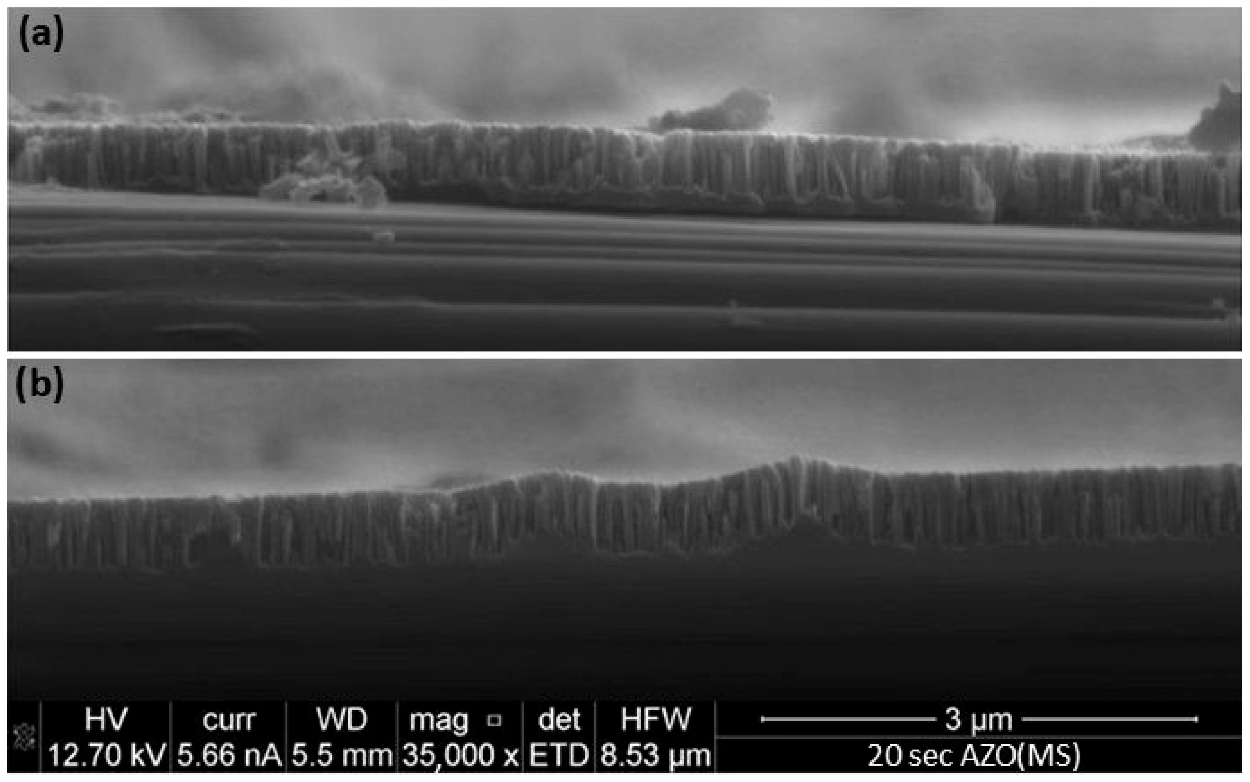
In addition to the atomic layer deposition of AZO films, we extended our study to include magnetron sputtering as an alternative deposition technique. While ALD offers unrivaled conformality and thickness control on high-aspect-ratio nanostructures, its inherently low growth rate and complex precursor chemistry can limit throughput and increase process cost. Magnetron sputtering, by contrast, provides higher deposition rates, simpler precursor handling, and proven scalability in industrial thin-film manufacturing. Moreover, the distinct energy and angular distribution of sputtered species can induce different microstructural features—such as columnar grain growth and enhanced optical scattering—that may prove advantageous for light trapping and charge extraction in tandem photovoltaic architectures. By comparing AZO layers grown by both ALD and magnetron sputtering on identical silicon nanowire scaffolds, we aim to elucidate how the deposition method influences film conformality, electrical conductivity, and interfacial quality, thereby informing optimal process selection for high-performance perovskite/silicon tandem solar cells. Cross-sectional SEM analysis at a 25,000× magnification of samples coated by magnetron sputtering reveals a markedly different coverage morphology compared to ALD-grown films. The results are presented in
Figure 4.
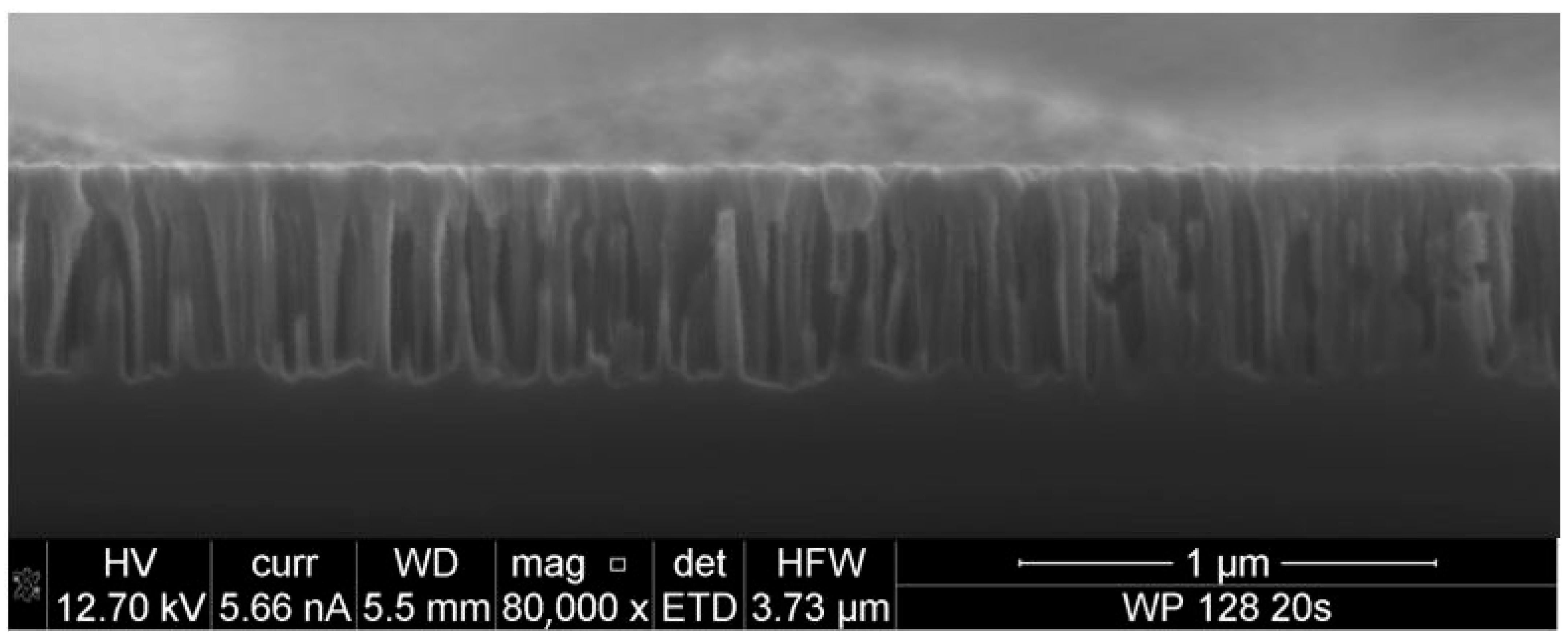
The sputtered AZO layer predominantly accumulates at the nanowire tips, forming partial caps while leaving significant gaps along the sidewalls. This non-conformal “line-of-sight” deposition is characterized by shadowing effects and reduced precursor penetration into the porous scaffold. Voids and uncovered regions observed in the lower half of the nanowires suggest that electrical continuity and charge recombination pathways may be compromised. These observations underscore the trade-off inherent in sputtering: while higher deposition rates and industrial scalability are achievable, the directional nature of the process limits uniform film growth on high-aspect-ratio structures and necessitates further optimization—such as substrate rotation or oblique angle sputtering—to improve conformality. To highlight the preferential accumulation of AZO at the nanowire tips, high-magnification SEM images were captured (
Figure 5).
Cross-sectional SEM (80,000×, HFW 3.73 µm) of a magnetron-sputtered AZO film on vertically aligned SiNWs reveals a pronounced “cap” of 50–100 nm thickness at the wire apexes, while the sidewalls would seem undercoated, and the lower forest is essentially bare. These results underscore the necessity of adapting sputtering parameters—e.g., substrate rotation or oblique angle deposition—to improve AZO coverage on high-aspect-ratio nanostructures.
3.2. TEM Analysis of AZO Thin Films on Silicon Nanowire Substrates
To comprehensively evaluate the thickness uniformity of the AZO coating along the full length of the silicon nanowires, transmission electron microscopy (TEM) was employed as a complementary technique to SEM. Whereas high-resolution SEM imaging offers detailed surface and cross-sectional morphology, TEM enables the direct visualization of the AZO/SiNW interface at the nanoscale, providing precise measurements of film continuity, crystallinity, and potential interfacial defects throughout the entire wire height.
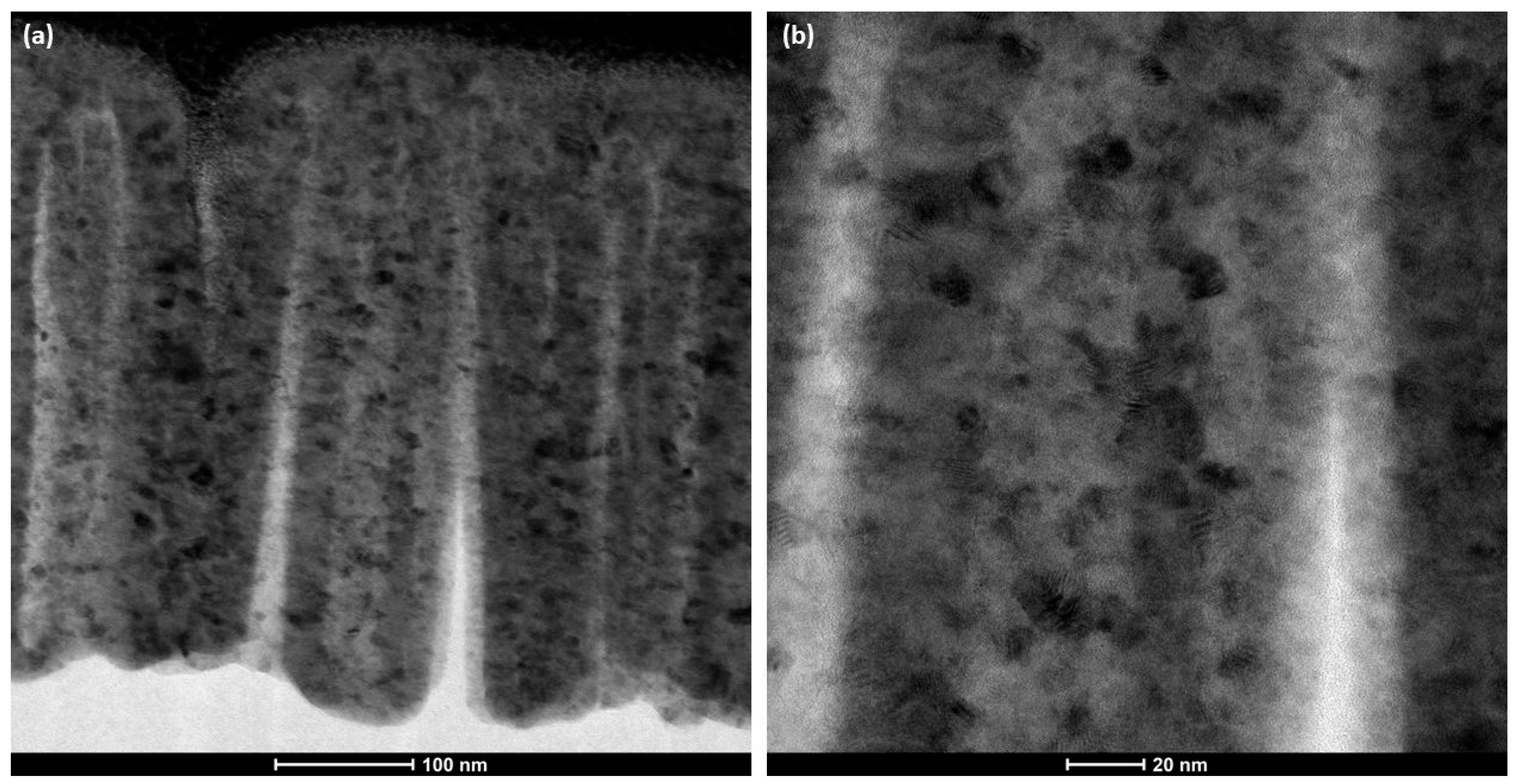
The bright-field TEM micrographs in
Figure 6 depict the AZO(ALD)-1 sample—an ALD-deposited Al-doped ZnO layer on silicon nanowire arrays.
Figure 6a shows the AZO film which appears as a uniform, conformal shell enveloping each nanowire, with an average thickness of ~40 nm and no observable voids at the interface.
Figure 6b offers a closer view of the AZO nanostructure: fine, polycrystalline ZnO grains (~5–10 nm in diameter) are visible, interspersed with darker contrast regions that likely correspond to Al-rich domains or slight amorphous intergranular material. The sharp AZO/Si interface and the homogeneous grain dispersion confirm the effectiveness of the ALD process in achieving continuous coverage and a controlled microstructure—even along high-aspect-ratio SiNWs—critical for ensuring efficient charge transport and minimal recombination losses in tandem solar devices.
The high-resolution TEM (HRTEM) image in
Figure 7 provides atomic-scale insight beyond the bright-field overview, revealing the crystallographic quality and defect structure of the ALD-grown AZO layer. Distinct lattice fringes with interplanar spacings of ~0.26 nm are clearly resolved, corresponding to the (002) planes of wurtzite ZnO, which confirms the preferential c-axis orientation of the ZnO crystallites. The uniform fringe contrast across the region indicates consistently sized grains (~5–10 nm) without large amorphous pockets, corroborating the grain size distribution inferred from lower-magnification TEM. At the AZO/Si interface (lower right), no transitional amorphous layer is observed, demonstrating a sharp, defect-free boundary crucial for efficient charge transfer. Occasional fringe disruptions suggest a low density of point defects or dislocations—likely associated with aluminum incorporation—which can modulate carrier concentration without significantly compromising crystal integrity. Overall, this HRTEM analysis validates that the ALD process yields a highly crystalline, uniformly doped AZO layer with excellent interfacial quality.
STEM–HAADF and the corresponding EDS elemental maps (Si, Zn, Al) provide a definitive, spatially resolved confirmation of both the AZO shell morphology and its compositional uniformity, extending the insights obtained from SEM and bright-field/TEM imaging. In the HAADF image (
Figure 8), the high-Z contrast clearly delineates the Si nanowire cores (brightest) from the surrounding AZO coating (intermediate gray) and the vacuum (dark). The Si map (green) precisely traces the nanowire positions, confirming intact wire geometry and revealing that the AZO film does not penetrate between the closely spaced wires. The Zn map (purple) shows a continuous, conformal shell enveloping each nanowire with nearly constant thickness, corroborating the ALD-driven uniformity inferred from TEM thickness profiles. Meanwhile, the Al map (yellow-green) demonstrates homogeneous dopant incorporation throughout the ZnO matrix, without observable clustering or segregation at the interface or within grain boundaries. Together, these data validate that the ALD process produces a uniform, doped ZnO layer on high-aspect-ratio SiNW scaffolds, with a sharp AZO/Si boundary and consistent elemental distribution.
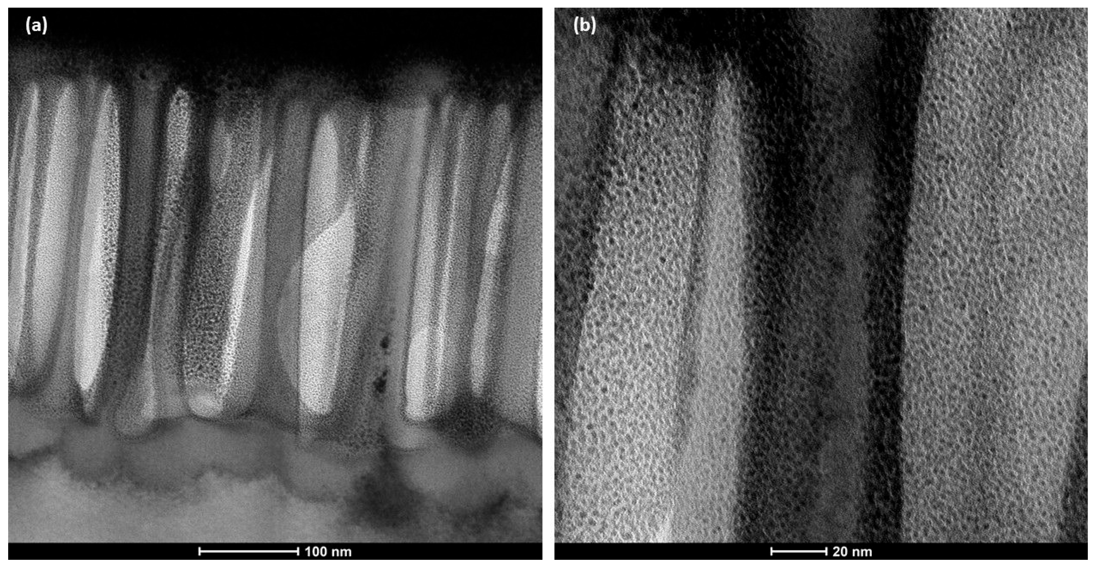
An identical TEM characterization workflow was applied to AZO layers deposited by magnetron sputtering, facilitating a direct nanoscale comparison with ALD-grown films. This side-by-side analysis enables the evaluation of coating conformality, grain structure, interface quality, and dopant distribution arising from the distinct deposition mechanisms.
The bright-field TEM images of the magnetron-sputtered AZO layer on SiNWs reveal a markedly different microstructure compared to the ALD sample. In
Figure 9a the AZO coating appears as an irregular, discontinuous shell: thick caps at the wire tips contrast with sparse, patchy coverage along the sidewalls, leaving voids at the wire bases.
Figure 9b shows that the sputtered film comprises larger, loosely packed ZnO grains (∼10–20 nm) with variable contrast—indicative of uneven Al incorporation and possible amorphous intergranular regions. The lack of a uniform, conformal shell and the presence of grain boundary gaps underscore the limited sidewall penetration characteristic of line-of-sight sputtering, which may hinder charge transport and recombination uniformity in the tandem cell architecture.
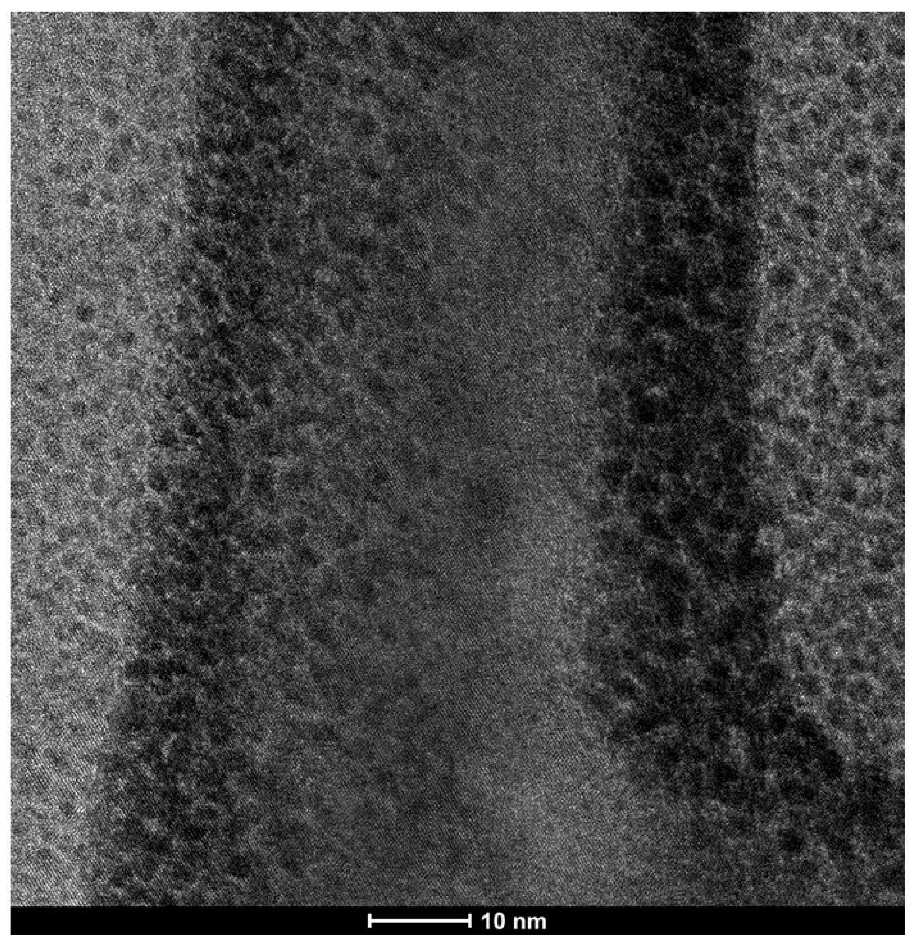
The high-resolution TEM micrograph (
Figure 10) of the magnetron-sputtered AZO on SiNWs reveals the fine details underlying the patchy coating observed in lower-magnification images. Here, the ZnO grains appear significantly larger (~10–20 nm) and more irregularly shaped than in the ALD sample, with poorly defined lattice fringes and regions of diffuse contrast that suggest the presence of amorphous or defect-rich intergranular material. Grain boundaries are prominent and unevenly distributed, correlating with the discontinuous sidewall coverage and voids seen in bright-field TEM. The uneven contrast across adjacent nanowire sidewalls confirms that sputtered species did not uniformly infiltrate the scaffold, instead aggregating into isolated columns. This image thus substantiates that magnetron sputtering produces a heterogeneous microstructure.
While magnetron sputtering exhibits limitations in conformally coating highly porous silicon nanowire scaffolds—manifesting as tip-dominant caps and incomplete sidewall coverage—this technique nonetheless offers advantages such as high deposition rates, industrial scalability, and distinct columnar microstructures that could be leveraged for enhanced light scattering or patterned coatings. The observed non-uniformity is therefore not an inherent flaw of sputtering itself but rather a consequence of the challenging high-aspect-ratio geometry; for such applications, atomic layer deposition remains the preferred method for ensuring complete, uniform coverage. However, sputtered AZO films may still prove valuable for complementary roles—such as surface texturing, seed layers for subsequent ALD, or in devices with less demanding conformality requirements.
3.3. Evaluation of AZO Layer Thickness
The accurate determination of AZO layer thickness is essential for optimizing the balance between electrical conductivity and optical transparency in perovskite/silicon tandem solar cells. Film thickness directly influences resistance—thicker films generally reduce resistive losses—and free carrier absorption, which can impair light transmission to the silicon subcell.
Film thickness was measured ex situ by the step height method using a Taylor Hobson CCI Lite optical profilometer. These measurements enable a direct comparison of conformality and growth rate between the two deposition methods and inform the selection of the process parameters (ALD cycle count or sputtering duration) needed to achieve the optimal compromise between optical and electrical performance in tandem device architectures. The results are presented in
Table 4.
The profilometry results summarized in
Table 4 demonstrate the precise, cycle-dependent control of AZO film thickness via ALD, with nominal values of 40 nm (AZO(ALD)-1), 65 nm (AZO(ALD)-2), and 120 nm (AZO(ALD)-3). In contrast, magnetron sputtering yields thicker baseline coatings—100 nm for AZO(MS)-1 and 120 nm for AZO(MS)-2—with less granular control over intermediate thicknesses. Notably, both ALD and sputtering can achieve the target ~120 nm film (AZO(ALD)-3 and AZO(MS)-2), but only ALD offers stepwise fine tuning across a wide thickness range. These findings underline that ALD is better suited when precise thickness adjustment is required, whereas sputtering provides a faster route to moderate-to-thick films when sub-50 nm resolution is not critical.
3.4. Optical Characterization of AZO Layers
In perovskite/silicon tandem solar cells, the optical properties of the intermediate recombination layer are critical: its visible and near-infrared transmission directly governs the fraction of incident sunlight that can penetrate into the underlying silicon subcell. A highly transparent recombination layer maximizes photocurrent in the bottom junction, boosting overall tandem efficiency. However, achieving both high electrical conductivity and excellent optical transmission in a single thin film is inherently challenging. Conductive oxide layers such as AZO must incorporate sufficient free carrier density to facilitate charge transport, yet excessive free carrier absorption and plasma reflection in the near-IR range can severely reduce transmittance. Balancing these competing demands—doping level, film thickness, and microstructure—thus represents a key materials engineering hurdle in the design of efficient recombination layers for perovskite/silicon tandems.
Transmission spectra were acquired with a Lambda 950S Perkin Elmer (Shelton, CT, USA) spectrometer halogen–deuterium light source with an integrating sphere in the wavelength range 300–1200 nm (ALD-deposited layers) and an Ocean Optics QE65000 spectrophotometer (Dunedin, FL, USA) coupled to a DH-BAL 2000 halogen–deuterium light source (Dunedin, FL, USA) over the 250–1000 nm wavelength range (MS-deposited layers).
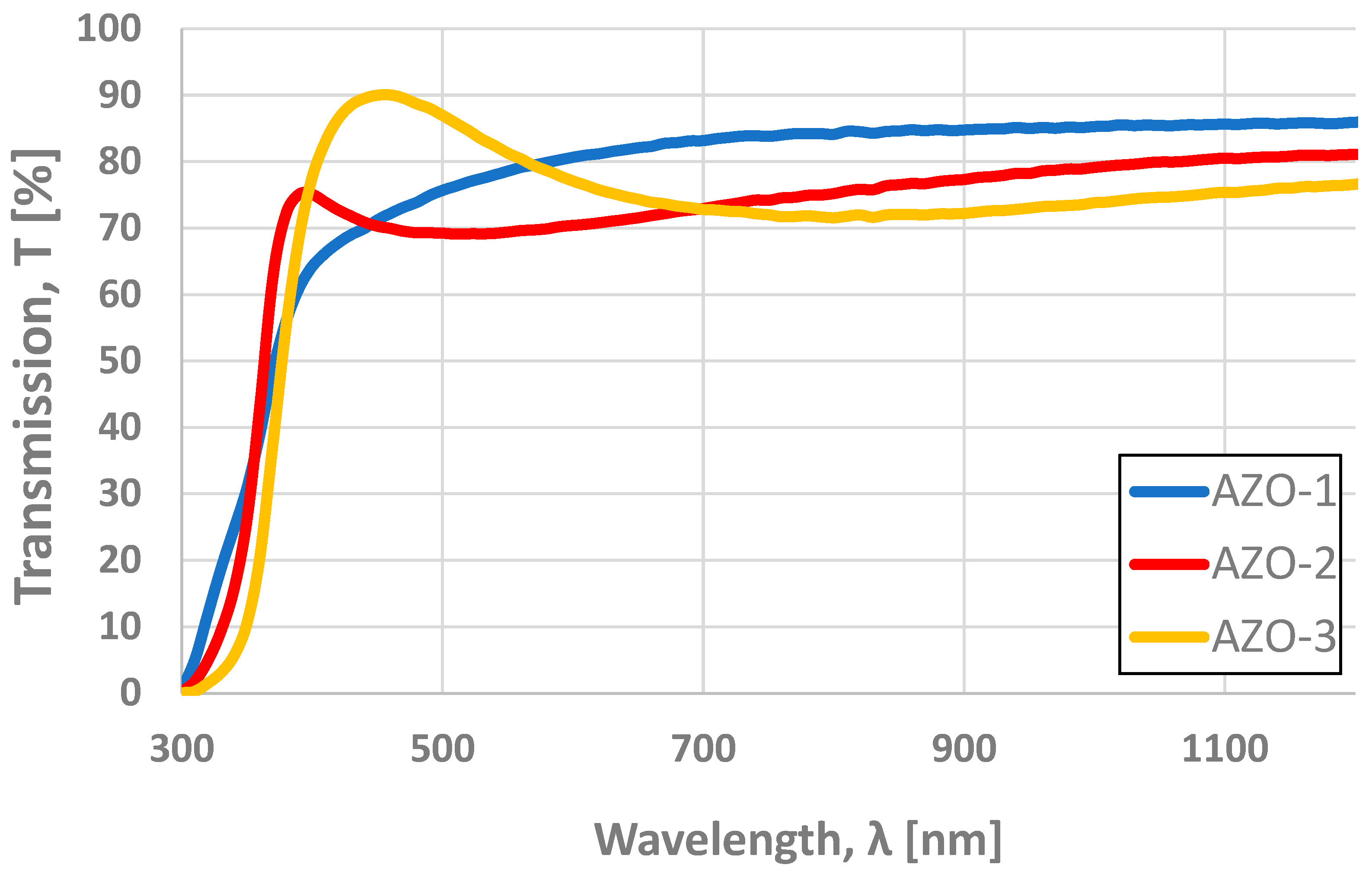
The optical transmission spectra of AZO films deposited by the ALD method on microscope glass (
Figure 11) exhibit pronounced thickness-dependent behavior that is critical for their function as recombination layers in perovskite/silicon tandem solar cells. The thinnest film, AZO(ALD)-1, achieves the highest broadband transparency, rising sharply from near zero at the ultraviolet cutoff to approximately 75% at 500 nm and plateauing between 82% and 86% across the 600–1100 nm region. Such high near-infrared transmittance is essential to ensure that sub-bandgap photons efficiently reach the silicon bottom cell. In contrast, the intermediate-thickness sample AZO(ALD)-2 displays a modestly reduced minimum transmission of ~69% at 500 nm and stabilizes around 76–80% in the near-IR range, reflecting increased free carrier absorption and interference effects. The thickest film, AZO-3, features a pronounced interference maximum near 450 nm (~90%), followed by a transmission dip to ~68% at 600 nm and a recovery to ~75–78% in the NIR range. While this visible-range enhancement is beneficial, the concomitant reduction in longer-wavelength transmission may constrain the photocurrent of the silicon subcell. These results underscore that, although thicker AZO layers can improve electrical conductivity, they also introduce optical losses that must be carefully balanced to maximize overall tandem device efficiency.
Similarly, the optical transmission of AZO films deposited by magnetron sputtering on glass substrates was evaluated under identical measurement conditions, enabling a direct comparison of the wavelength-dependent transparency and interference behavior imparted by each deposition technique.
The transmission spectra of magnetron-sputtered AZO films (
Figure 12) exhibit a different optical signature compared to their ALD-deposited counterparts. Both the AZO(MS)-1 and AZO(MS)-2 samples show a sharp UV cutoff near 350 nm, but the interference peak around 450–500 nm is significantly more pronounced—reaching over 90% for the thicker AZO(MS)-2 film—than in the ALD layers. Beyond this visible-range maximum, the sputtered films settle to a steady 80–85% transmission in the near-IR range (700–1000 nm). This behavior reflects the columnar microstructure and greater thickness of the MS coatings, which enhance constructive interference in the visible band yet incur modest additional free carrier absorption at longer wavelengths.
Notably, the transmission spectrum of the ≈120 nm AZO(ALD)-3 film (
Figure 11) closely mirrors that of the ≈120 nm AZO(MS)-2 coating (
Figure 12), with both exhibiting a pronounced interference maximum around 450–500 nm and settling to comparable near-IR transparencies (~80–85%), underscoring that ALD-grown layers of similar thickness can achieve optical performance on par with magnetron-sputtered films.
3.5. Electrical Characterization of AZO Layers
To evaluate the charge transport properties of the AZO recombination layers, we conducted electrical characterization on films deposited concurrently with those used for optical measurements.
Surface resistance was measured using a Jandel Engineering four-point probe head (Jandel Engineering Ltd., Buzzard, UK) with 1 mm spaced tungsten carbide tips, coupled to a Keithley 2611A source measure unit (Keithley Instruments Inc., Solon, OH, USA). The outer probes supplied the current, while the inner probes recorded the voltage drop.
Four-point probe measurements were performed on AZO coatings deposited on SiO
2 dielectric substrates to determine surface resistance as functions of film thickness and deposition method. This electrical parameter is critical for assessing the trade-off between transparency and conductivity in recombination layers: high carrier density and mobility are required to minimize resistive losses, while excessively thick or heavily doped films can compromise optical transmission. By comparing ALD and magnetron-sputtered AZO samples under identical conditions, we establish a comprehensive view of how deposition technique and film thickness influence the electrical performance of tandem solar cell interfaces. The results are presented in
Table 5.
The surface resistance data reveal a clear dependence of electrical conductivity on both film thickness and deposition method. For the ALD-grown layers, increasing the cycle count from AZO(ALD)-1 to AZO(ALD)-3 reduces the surface resistance from 1150 Ω/□ to 245 Ω/□, consistent with thicker films supporting higher carrier densities and more continuous conduction pathways. Magnetron-sputtered samples fall between the ALD extremes: AZO(MS)-1 (648 Ω/□) outperforms the thinnest ALD film but underperforms AZO(ALD)-2, whereas AZO(MS)-2 (317 Ω/□) achieves conductivity on par with the thickest ALD coating. Notably, both AZO(MS)-2 and AZO(ALD)-3 share an estimated thickness of approximately 120 nm and exhibit similar electrical parameters, underscoring that similar layer dimensions yield comparable surface resistances regardless of deposition technique. These trends highlight the classic trade-off in recombination layer design: thicker or more heavily doped films improve electrical transport but can introduce optical penalties. The comparable performance of AZO(MS)-2 and AZO(ALD)-3 suggests that sputtering can be a viable route to low-resistance layers—albeit with the conformality limitations noted earlier—while ALD offers superior thickness control and uniformity at the expense of longer processing times.
3.6. A Summary of Optical and Electrical Properties as a Function of AZO Layer Thickness and Deposition Method
To enable a direct comparison of optoelectronic performance across deposition methods and film thicknesses,
Table 6 compiles the near-infrared transmission (800–1200 nm), measured layer thickness, and four-point probe surface resistance for all AZO samples.
Table 6 summarizes the key optoelectronic properties of AZO films deposited by ALD and magnetron sputtering. For each sample, the near-infrared transmission range (800–1200 nm) is reported alongside the measured layer thickness and four-point probe surface resistance. The data reveal that thinner ALD films (40–65 nm) offer superior NIR transparency (75–86%) but exhibit higher surface resistance (276–1150 Ω/□), whereas thicker coatings (~120 nm) achieve lower resistances (245–317 Ω/□) at the expense of modestly reduced transmission (72–86%). Magnetron-sputtered layers display comparable transmission and resistance to their ALD counterparts at similar thicknesses, highlighting that both deposition methods can be tuned to balance optical and electrical performance for tandem solar cell recombination layers.
4. Discussion
The comparative evaluation of AZO layers deposited by ALD and magnetron sputtering on silicon nanowire (SiNW) scaffolds reveals a nuanced interplay between deposition method, film morphology, and optoelectronic performance. This relationship is central to the design of efficient perovskite/Si tandem cells. SEM investigations (
Figure 1,
Figure 2 and
Figure 3) show that ALD yields uniformly conformal shells along the wire length—even at 120 nm thickness—whereas magnetron sputtering (
Figure 4 and
Figure 5) produces pronounced “match-head” caps and undercoated sidewalls. Height profiling (
Table 3 and
Table 4) quantifies the following: ALD films grow from an average 464 nm total structure height at 40 nm overlayer to 560 nm at 120 nm, with minimal void formation except in localized overgrowth zones. In contrast, sputtered films of comparable thickness (100–120 nm) exhibit non-uniform coverage, leaving voids that may disrupt charge percolation pathways.
Optically (
Figure 11 and
Figure 12), the thinnest ALD sample achieves 84–86% transmission in the 800–1200 nm window, dropping to 72–77% at 120 nm (AZO-3), while sputtered films maintain 83–89% transmission over the same range. The pronounced interference peaks around 450–500 nm in both AZO(ALD)-3 and AZO(MS)-2 underscore that sufficiently thick films—regardless of method—can enable equivalent light management properties. Electrically (
Table 5), surface resistance falls sharply from 1150 Ω/□ at 40 nm to 245 Ω/□ at 120 nm in ALD films; sputtered layers bracket these values at 648 Ω/□ (100 nm) and 317 Ω/□ (120 nm). The direct correspondence between ≈120 nm ALD and sputtered films (245 vs. 317 Ω/□) confirms that similar thicknesses yield comparable conductivity, even though their microstructures differ markedly.
Taken together, these data support several key conclusions. First, ALD is uniquely able to produce defect-free, conformal AZO coatings that minimize interfacial trap sites and ensure continuous recombination pathways—critical for avoiding resistive losses and shunting in tandem architectures. Second, magnetron sputtering, while less conformal on high-aspect-ratio SiNWs, can still deliver low-resistance, highly transparent films when thickness is matched, suggesting a role in hybrid strategies (e.g., as a rapid seed layer prior to ALD overcoat or in planar regions of the device). Third, the clear thickness–performance correlations evident in both optical (transmission vs. free carrier absorption) and electrical (resistance vs. carrier density) metrics point to an optimal AZO window around 100–120 nm for balancing transparency and conductivity.
Looking forward, integrating these AZO variants into fully processed tandem cells will be essential to translate material-level advantages into device efficiency gains. Future work should explore dynamic sputtering geometries (e.g., substrate rotation, glancing incidence). Dopant co-incorporation strategies (e.g., Ga or In) and post-deposition annealing regimes should also be investigated to refine microstructure, enhance dopant activation, and reduce resistive and optical losses. Such efforts will be critical for realizing AZO-based recombination layers that combine the throughput advantages of sputtering with the conformality and uniformity intrinsic to ALD.
