1. Introduction
The quest for higher efficiency in solar cell technology has driven numerous innovations and research endeavors over the past few decades. Multi-junction solar cells (MJSCs) stand at the forefront of this technological evolution, capturing a broader spectrum of sunlight by stacking multiple semiconductor materials with varying bandgaps. This approach significantly surpasses the efficiency of traditional single-junction solar cells. Historically, MJSC development has been marked by milestones, starting with Edmond Becquerel’s discovery of the photovoltaic effect in 1839 and Bell Labs’ creation of the first practical silicon solar cell in 1954, which achieved an efficiency of around 6% [
1,
2].
As the world grapples with energy security and environmental sustainability, advancing solar cell technology is crucial [
3]. The oil crises of the 1970s underscored the urgency for alternative energy sources, propelling solar technology to the forefront of renewable energy research [
4]. This period saw the rise of polycrystalline silicon cells, offering a more cost-effective solution compared to monocrystalline silicon cells [
5], marking a significant step towards commercializing solar technology. The late 20th and early 21st centuries witnessed remarkable advancements in materials science, leading to thin-film solar cells and other technologies that enhanced efficiency and reduced manufacturing costs [
6]. Among these, Copper Indium Gallium Selenide (CIGS) has garnered significant attention due to its tunable bandgap and superior absorption properties for long-wavelength photons. CIGS can potentially replace traditional germanium (Ge) substrates in MJSCs, broadening the absorption spectrum and further elevating overall cell efficiency [
7].
Our research focuses on optimizing five-junction solar cells composed of AlInP, AlGaInP, AlGaInAs, GaInP, GaAs, InGaAs, and Ge using advanced predictive modeling and cutting-edge CIGS integration techniques. By employing Silvaco TCAD tools and sophisticated statistical models, we aim to enhance the electrical performance and efficiency of these cells. The intricate relationship between layer thickness and electrical yield under one-sun illumination is analyzed comprehensively, potentially setting new benchmarks in solar cell efficiency. The development of MJSCs addresses the efficiency limitations of single-junction solar cells, which are constrained by the Shockley–Queisser limit and can theoretically convert only about 33.7% of incident solar energy into electricity. In contrast, MJSCs, by utilizing multiple layers of semiconductors with different bandgaps, can achieve efficiencies exceeding 40% [
8]. Each layer absorbs a specific portion of the solar spectrum, minimizing energy losses due to the thermalization of charge carriers.
The objectives are multi-faceted: optimizing layer thickness using advanced statistical modeling and predictive profiling tools to determine the optimal thickness of each layer within the MJSC structure to maximize electrical yield; investigating the impact of replacing the Ge substrate with CIGS on the overall performance and efficiency of the MJSC; and conducting comprehensive performance evaluations using Silvaco TCAD simulations to assess the electrical characteristics and efficiency improvements brought about by the optimized and CIGS-integrated MJSCs [
9].
To achieve these goals, genetic algorithms (GAs) are employed for optimization. GAs are particularly effective in solving complex multi-dimensional problems by iterating through generations of potential solutions [
10]. In this context, GAs generate a diverse set of potential solutions, evaluate them using a predefined objective function [
11], and iteratively improve them through mathematical operations such as selection, recombination, and variation to find the optimal configuration. This method significantly accelerates the optimization process compared to traditional brute-force methods. The statistical modeling involved employs advanced computational techniques to ensure precise and reliable predictions [
12,
13]. By leveraging the capabilities of high-performance computing systems and sophisticated software tools, the study achieves a high level of accuracy and efficiency in modeling solar cell performance.
The strategic integration of CIGS in place of Ge as the bottom cell material leverages the superior optoelectronic properties of CIGS [
14,
15,
16,
17,
18]. The CIGS bandgap tunability (ranging from 1.0 to 1.7 eV) and high absorption coefficient make it an ideal candidate for capturing low-wavelength photons that are otherwise inefficiently absorbed by traditional materials. This substitution improves overall spectral absorption and enhances the power conversion efficiency (PCE) of the MJSC [
19,
20]. This comprehensive approach underscores the critical importance of advanced materials and precise engineering in driving the next generation of solar cell technologies, setting the stage for further breakthroughs in renewable energy efficiency.
In addition to optimizing material properties and structural configurations, this study also emphasizes the importance of innovative modeling techniques. The use of Silvaco TCAD tools allows for detailed simulations of the electrical characteristics of the MJSCs [
21,
22], providing insights that are crucial for further improvements. These tools enable the simulation of various parameters, including spectral absorption, current–voltage characteristics, and overall efficiency under different conditions. By integrating these advanced simulation techniques with genetic algorithms, the research achieves a synergistic effect that enhances the overall effectiveness of the optimization process.
The role of statistical analysis in this context cannot be overstated. By employing techniques such as regression analysis [
23], correlation studies, and predictive modeling, the study ensures that the optimization process is both rigorous and data driven. These statistical methods provide a robust framework for analyzing the complex relationships between different variables, leading to more accurate and reliable results. The integration of machine learning frameworks further enhances the predictive capabilities of the study, enabling the development of models that can adapt to new data and improve over time.
Overall, this research represents a significant step forward in the field of solar cell technology. By combining advanced materials, innovative modeling techniques, and sophisticated statistical methods, it sets the stage for the development of next-generation solar cells that offer higher efficiency and greater reliability. The findings of this study have the potential to drive further advancements in the field, paving the way for more sustainable and efficient solar energy solutions in the future.
2. Materials and Methods
2.1. Device Structure and Modeling Approach
In our recent exploration of solar cell technology, we embarked on a journey to optimize solar cell design, beginning with a sophisticated physical model grounded in the fundamental principles of semiconductor physics [
24]. This model acted as a detailed map, charting the interactions of light particles (photons) with electricity carriers (electrons and holes) within the layers of the solar cell. Our approach was methodical, resembling the process of solving a complex puzzle, where we meticulously calibrated parameters such as doping concentrations and layer thicknesses to mirror real-world conditions. This careful calibration aimed to align our model with the actual behavior of solar cells, specifically focusing on their current density and open-circuit voltage, which are critical indicators of a cell’s power output [
25].
Delving deeper into the heart of the solar cell, we modeled each component: the protective window layer, the protective window layer, the light-absorbing emitter, the sturdy base, the efficiency-boosting back surface field (BSF), and the stabilizing buffer [
26]. Each component played a pivotal role in converting sunlight into electricity, akin to gears in a finely tuned machine. Our initial modeling took into account the unique properties of each material, their effectiveness in capturing light, and the dynamics of electricity flow. The material selection process was analogous to choosing the right ingredients for a gourmet recipe, where materials were chosen not only for their compatibility with the cell’s structure but also for enhancing its performance under real solar conditions [
27,
28].
Our research began by examining a five-junction structure documented in the existing literature, which provided baseline data on electrical efficiency [
29,
30]. At the core of our innovation was the integration of statistical tools to determine an optimal yield for the thickness of the optimal region. We utilized both Silvaco TCAD and Python simulations to compile a large dataset linking layer thickness with electrical efficiency. This effort enabled us to develop a predictive mathematical model to facilitate the easy determination of optimal layer thicknesses in future designs.
A significant milestone in our research was the decision to replace the last germanium (Ge) layer of this structure with Copper Indium Gallium Selenide (CIGS) [
31,
32,
33]. This change was influenced by the unique properties of CIGS, such as its tunable bandgap and superior absorption of long-wavelength photons, expected to significantly enhance the overall efficiency of the solar cells. The total thickness of our multi-junction cell, excluding the active germanium substrate at the bottom, was precisely 2.525 μm, reflecting the high degree of engineering precision that went into the design. This meticulous attention to detail was crucial in accounting for the cell’s optical and electrical properties, ensuring our model was robust enough to accurately predict its real-world performance.
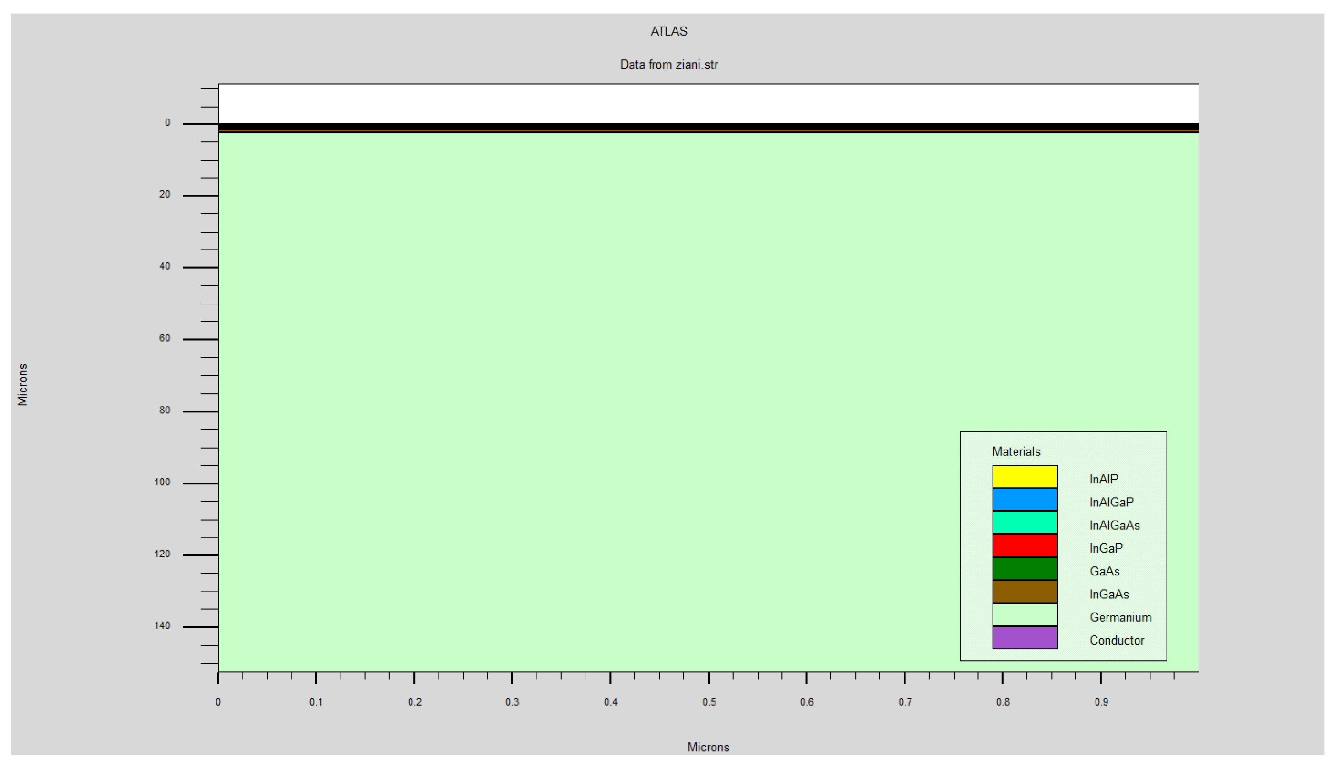
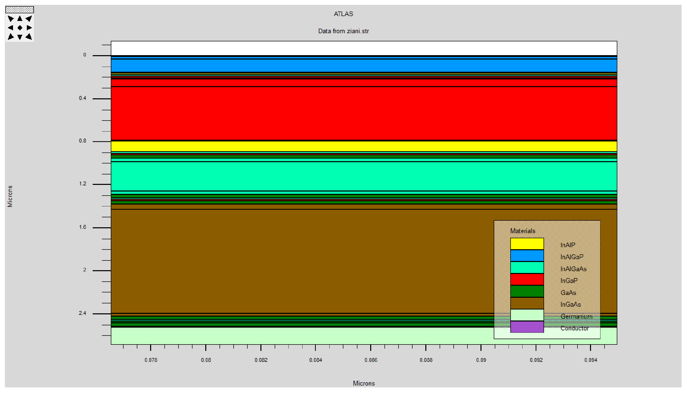
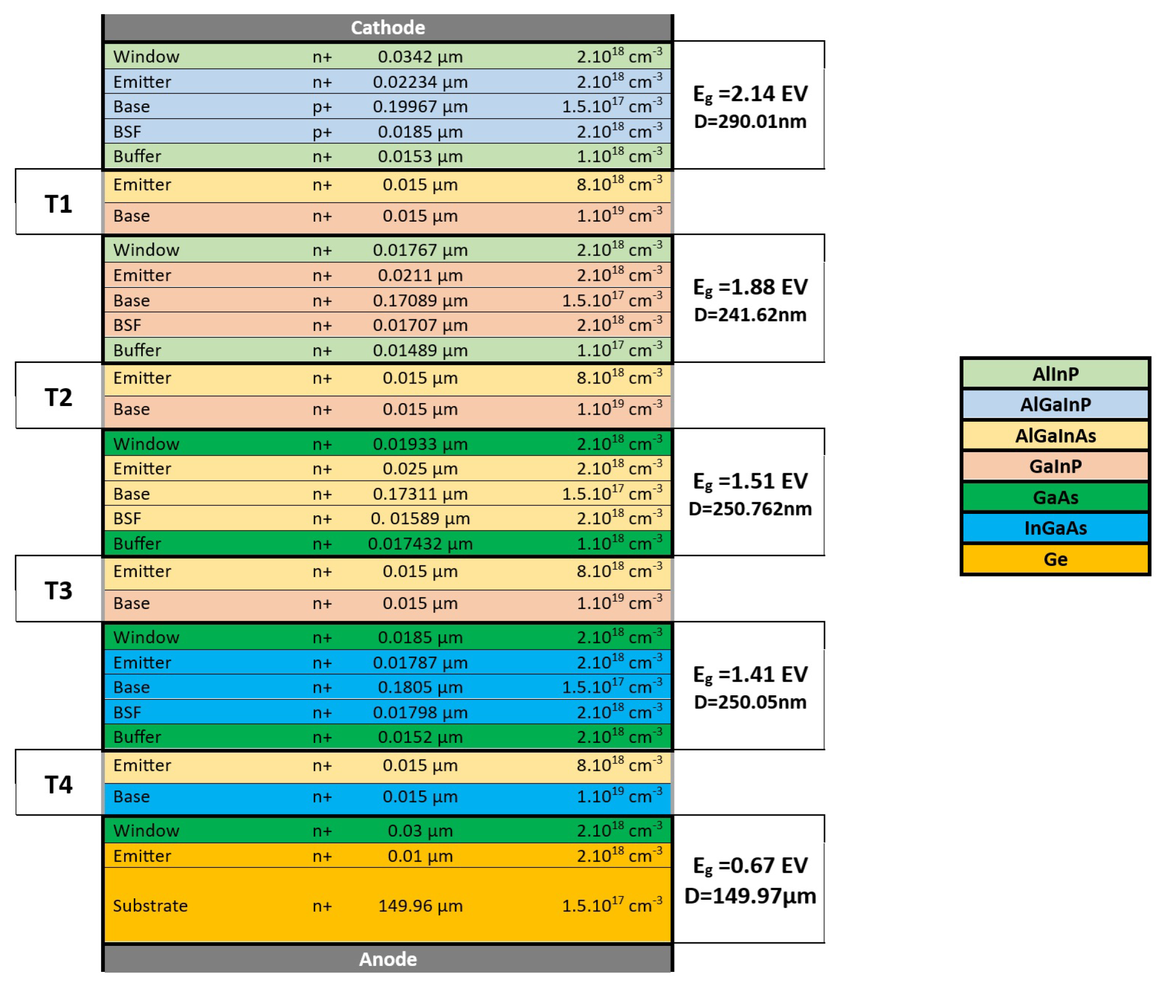
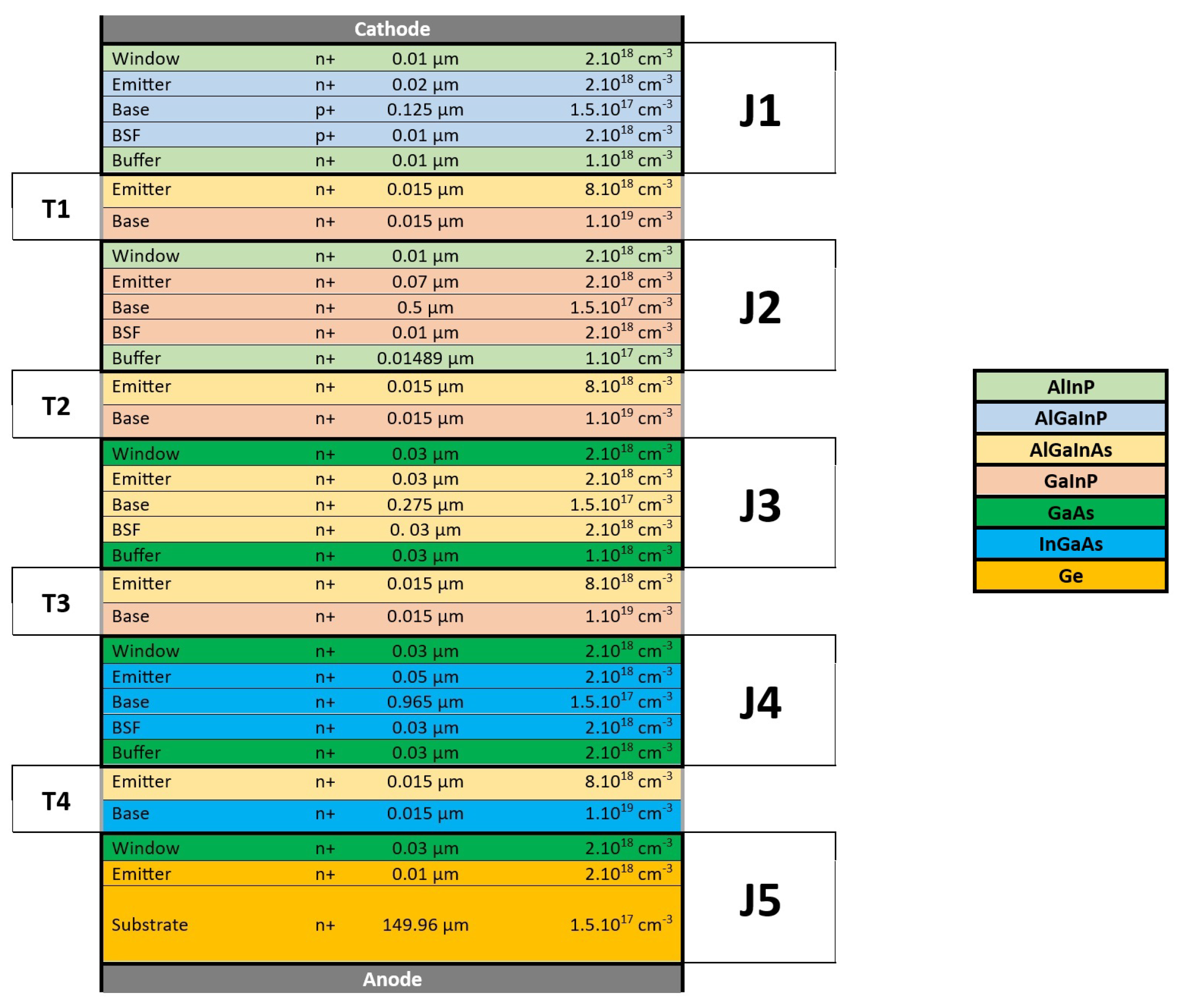
In our quest to optimize multi-junction solar cells as shown in
Figure 1, we utilized the powerful capabilities of Silvaco Atlas simulation software [
34,
35]. This tool acted as a master key, unlocking the complex relationship between the thickness of each solar cell layer and its doping concentrations. This intricate interplay of variables is crucial for the efficiency of the cell. Let us visualize this process. Imagine each layer of the solar cell as a tier in a cake, where the specific thickness and “ingredients” (doping concentrations) of each layer significantly influence the overall effectiveness (efficiency) of the solar cell [
36,
37,
38,
39]. To master this recipe, we delved into the realm of semiconductor physics equations. We began with the continuity equations for electrons (n) and holes (p), the fundamental particles in our solar cell narrative [
40]:
These equations, namely, Equations (
1) and (
2), act like the conductors of an orchestra, ensuring that the movement and interaction of these particles contribute harmoniously to the cell’s function. Next, we considered the Poisson equation, which plays a pivotal role in illustrating the electric field within the cell [
41,
42].
Equation (
3) sets the stage for the electrons and holes, guiding their movements across the cell’s layers [
43]. We also applied the drift–diffusion relations for current densities to model how these charge carriers move [
44]:
The relations of Equation (
4) are akin to choreographing a dance, directing each electron and hole in a synchronized flow to efficiently produce electricity [
45]. An optical model was also integrated, described by the simple yet crucial Equation (
5):
where
is the absorption coefficient, and
I is the incident light intensity. This model establishes the optimal conditions for light absorption, much like adjusting the spotlight on our solar cell stage [
46,
47,
48,
49]. The simulation brought together various models and parameters, each like a specialized tool in our toolbox, to accurately represent physical phenomena such as recombination, mobility, bandgap narrowing, and temperature effects. Through a series of iterative refinements, we identified an optimal configuration that maximized the cell’s energy yield, akin to finding the perfect balance in a complex recipe. This process was not merely about numbers and equations; it was a fusion of science, technology, and creativity, culminating in a solar cell that not only met but surpassed industry standards [
50].
Figure 1.
Reference structure of multi-junction solar cells: design and optimization [
51,
52].
Figure 1.
Reference structure of multi-junction solar cells: design and optimization [
51,
52].
2.2. Optimizing Solar Cell Design
Genetic algorithms initiate the optimization of solar cell design by generating a diverse population of random designs. Think of this as sowing a field with a variety of seeds [
53,
54,
55]. The process then evolves these designs through a series of selections, cross-breeding, and mutations, each step aimed at enhancing performance. We use sophisticated techniques like tournament selection to choose the best designs, uniform crossover to combine features, and Gaussian mutation to introduce variations. What really accelerates the discovery of optimal designs is a strategy known as elitism ensuring that the best performers consistently advance. Next, we employ NOLH (Nearly Orthogonal Latin Hypercube) sampling [
56,
57,
58]. This method is akin to carefully selecting points across our design field that offer the most diverse and comprehensive insights. It uses a statistical approach to ensure that the coverage of the design space is as efficient as possible, minimizing any correlation effects between variables. This broad and efficient coverage is crucial in fitting accurate response surface models, like polynomials [
59], which serve as guides in our optimization journey. Our toolkit also includes advanced methods such as artificial neural networks, support vector machines, and nature-inspired algorithms [
60]. Neural networks excel at modeling complex, nonlinear responses, learning from data much like a brain absorbing information. Swarm algorithms, such as particle swarm optimization, mimic the collective behavior of flocks or swarms, exploring the design space in a coordinated, intelligent manner. We often turn to hybrid approaches, combining the strengths of different techniques. For instance, a genetic or swarm algorithm might scan the design landscape from a bird’s-eye view for global optimization, while gradient-based methods zoom in on specific areas to fine-tune details for local optimization. We also employ statistical methods to account for uncertainty and variability, ensuring a comprehensive understanding of the design space. The power of high-performance computing cannot be overstated in this process. It allows us to run parallel simulations at an extraordinary scale, rapidly evaluating countless designs [
61]. Machine learning algorithms act as our guides, helping to steer the optimization based on insights drawn from the data [
62,
63,
64]. Underpinning all this is our trust in validated physics-based models, which ensure that our performance mapping remains grounded in reality [
65]. Finally, the optimization journey culminates in the thorough characterization and failure analysis of the prototypes. Techniques like Scanning Electron Microscopy (SEM) and External Quantum Efficiency (EQE) assessments provide invaluable feedback. This feedback loops back into our models and designs, fueling a cycle of continuous improvement. As we harness these advanced techniques, the frontier of solar cell optimization keeps advancing, offering increasingly efficient and effective solar energy solutions [
66].
Genetic Algorithms
In the realm of optimizing solar cell designs, genetic algorithms embody nature’s own survival-of-the-fittest principle [
53,
67]. Envision these algorithms as skilled gardeners selectively pruning a tree, where each branch represents a potential design path. This technique begins with a set of randomly generated initial parameters, the seeds from which potential solutions grow. It then evolves iteratively in a process akin to natural selection but adapted for the algorithmic world. This process is stochastic and nonlinear, emphasizing clever guesses and adaptability over strict, rigid mathematical rules. Applying this to solar cells, key elements like doping concentration and layer thickness can be likened to genes within a ‘chromosome’ of the solar cell design. Each chromosome is tested in the simulation environment, similar to observing how well a plant thrives under specific conditions. This testing phase helps us identify the most effective solutions—the designs that best meet our criteria [
68]. The process is iterative and dynamic
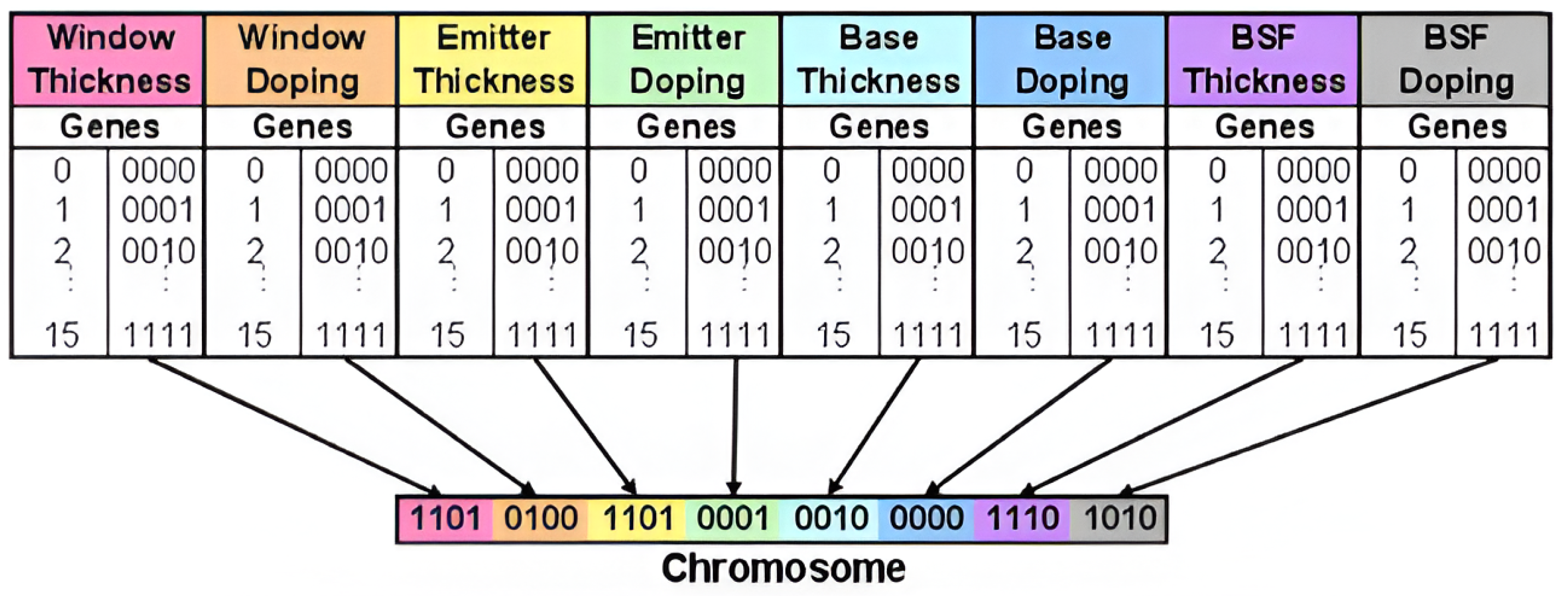
Figure 2. The best ’genes’ (or design parameters) from the current generation are carried over to the next, akin to how desirable traits are passed on through natural selection. Simultaneously, less effective solutions are discarded, ensuring continuous improvement. An intriguing method introduced by Bates involved using just four binary bits to represent each parameter, resulting in 16 possible variations for each one. An illustrative example of such a chromosome, used by Bates, is shown in the accompanying figure, providing a glimpse into the elegant simplicity of this method [
53,
67,
69].
Figure 2.
Chromosome configuration example used in Bates’ study [
70,
71].
Figure 2.
Chromosome configuration example used in Bates’ study [
70,
71].
2.3. Structural Parameters
In our simulation process, we utilized a range of materials, each with its unique properties. Consider each material as an actor in a play, with each one playing a specific role based on its characteristics. To manage these diverse roles, we outline their attributes using specific material statements, akin to a script that details each actor’s part.
For those interested in the finer details, the exact values we used for these materials are listed in
Table 1,
Table 2 and
Table 3. This is comparable to a recipe book that lists all the ingredients and their precise measurements. Moreover, if you are curious about why we chose these particular values or how each contributes to the overall performance of the solar cell, we provide a detailed discussion of each parameter. This discussion offers insights into the rationale behind each choice and how they impact the outcome of the simulation.
3. Results and Discussions
3.1. Solar Cell Structure with Five Tandem Junctions
The results obtained from simulating a multi-junction structure with five distinct band gap junctions, performed using SILVACO Atlas, are illustrated in the figures above
Figure 3 and
Figure 4. These figures highlight the tunnel effect zone for each junction, with the Ge substrate being a particularly notable element.
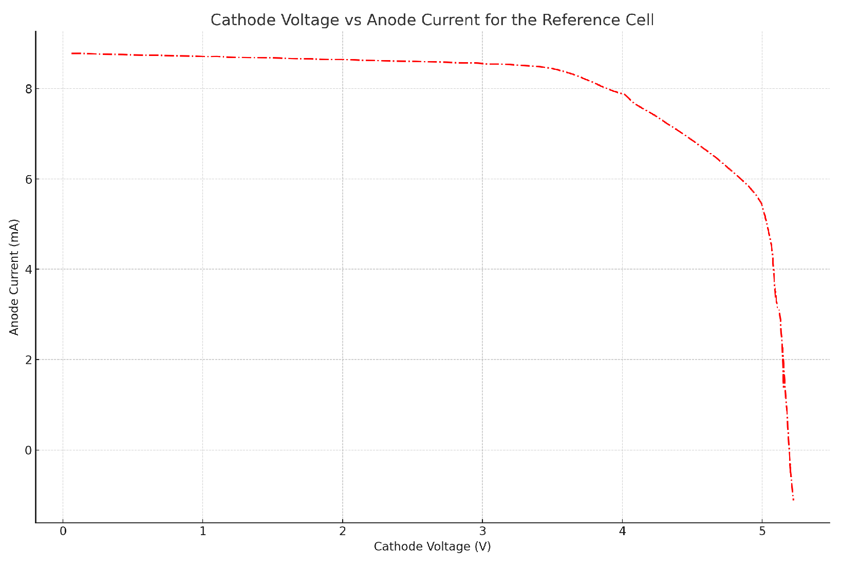
Characteristic I = f(v)
In our exploration of the solar cell’s performance through simulation, we translated its electrical behavior into visual stories as shown in
Figure 3 and
Figure 4. These figures are like snapshots, capturing the IV characteristic curve and the power–voltage relationship of the cell. It is a way of seeing, rather than just calculating, how the cell behaves under various conditions. For those who delve into details,
Table 1,
Table 2 and
Table 3 outline the critical values and parameters that form the backbone of our study. One aspect that immediately stands out is the solar cell’s fill factor, a modest 65.97%. This number serves as a health check, revealing the cell’s efficiency in converting sunlight to power. Its depiction on the IV curve as a subdued maximum power point is a telltale sign that warrants further investigation. It suggests there might be some hidden inefficiencies in the cell’s design or material properties that need addressing. Another key finding is the open-circuit voltage, which stands at 5.26026 V as shown in
Figure 5.
These benchmark results have prompted us to conduct a comprehensive statistical analysis to determine the ideal thickness for optimal performance. This predictive study employs a complex algorithmic method, utilizing predictive approaches in statistical models. It aims to incorporate rigorous quantitative analysis, allowing for the modeling and predicting of the performance of solar cells with increased accuracy. By adjusting the thickness of the cells based on the data obtained, we hope to maximize the conversion efficiency while minimizing losses due to internal inefficiencies.
The accompanying diagram, specifically
Figure 6, serves as a visual guide to the complex world of solar cell design. It illustrates how varying the thickness of each layer in our tandem junctions correlates with the overall efficiency of the cell. Imagine each layer as a unique ingredient in a recipe, where even a slight change in amount can affect the final dish’s flavor. This intricate layering, filled with subtle interdependencies and complex interactions, makes it challenging to pinpoint the perfect model for the cell’s structure. Determining the optimal thickness for each layer to maximize efficiency is not just a technical task; it is a deep dive into the heart of solar cell physics. However, when we examine the graph closely, with a keen eye for detail and a solid grasp of the physics involved, we begin to discern patterns emerging from the complexity. For instance, Junction 1 shows promising efficiency in the range of 0 to 0.2 μm. This insight might just open new doors in solar cell research. Junction 2 reveals its best performance in two specific intervals 0 to 0.2 μm and 0.6 to 0.8 μm, beckoning further exploration. Similarly, we find that Junction 3 performs well between 0 and 0.6 μm, while the final junction seems to hit its stride within a narrow range of 0 to 0.2 μm. These findings, subtle yet significant, could be crucial keys to unlocking new advancements in solar cell technology.
Previous research in the field of solar cell technology has often focused on identifying the ideal thicknesses for each layer within the cell’s structure. These ideal ranges are not arbitrary; they result from meticulous studies aimed at achieving the highest possible efficiency. Researchers have carefully analyzed the performance of each part of the solar cell, from the protective outer layers to the core where sunlight is converted into electricity. The approach typically involves running a series of simulations or experiments, varying the thickness of each layer within certain ranges. The efficiency of the cell is then measured for each variation. Over time, these measurements reveal patterns; certain thickness ranges consistently lead to better performance. By compiling and comparing these results, researchers have been able to provide guidance on the optimal thickness for each layer of a solar cell.
In our current work, we aim to advance this research further. We are utilizing advanced statistical techniques of correlation and prediction to determine more precise values for the thickness of each layer. This approach involves a detailed analysis of simulation data to identify deeper connections between layer thickness and cell efficiency. By applying predictive statistical models, we can forecast how subtle variations in each layer’s thickness affect the overall performance of the cell. Our goal is to move beyond the established range-based guidelines and pinpoint exact measurements for optimal efficiency. This pursuit of precision could lead to breakthroughs in solar cell efficiency, paving the way for more effective and economical solar energy solutions.
3.2. Statistical Model
In the realm of solar cell technology, we are undertaking a meticulous mission to optimize multi-junction tandem solar cells [
72,
73]. This task involves precisely calibrating each layer’s thickness, a crucial factor in maximizing the cell’s overall efficiency. Our tools for this intricate endeavor are predictive modeling and data partitioning, sophisticated techniques essential for refining the design of these solar cells. The optimization process begins by categorizing our data into two distinct sets. The first set, the training data, serves as our experimental ground. Here, we adjust and test various configurations, manipulating the thickness of each solar cell junction to gauge its impact on efficiency. The second set, the validation data, functions as our real-world testbed. We apply our models to these untouched data to simulate actual performance conditions, ensuring that our designs are not only theoretically sound but also practically viable [
74]. Throughout this iterative process, we continuously refine our machine learning models. This refinement is akin to a scientist conducting repeated experiments, each time honing in on the most effective configuration. We explore the vast design space of these solar cells, identifying the delicate balance between the different junctions. Each adjustment is a step towards discovering an optimal design that achieves the highest possible efficiency.
However, our exploration goes beyond merely adjusting existing models. We are pioneering new approaches, combining established methods with cutting-edge techniques. We delve into uncharted territories of layer thicknesses and material compositions, seeking innovative solutions that enhance solar cell performance. This approach represents a significant advancement in solar cell technology. We are not just incrementally improving designs; we are pushing the boundaries of what is possible, using data-driven predictive modeling to spearhead the development of next-generation solar cells. Our work aims to elevate solar energy from a mere option in the renewable energy landscape to a leading solution, harnessing the sun’s power more efficiently than ever before. This is illustrated in
Figure 7.
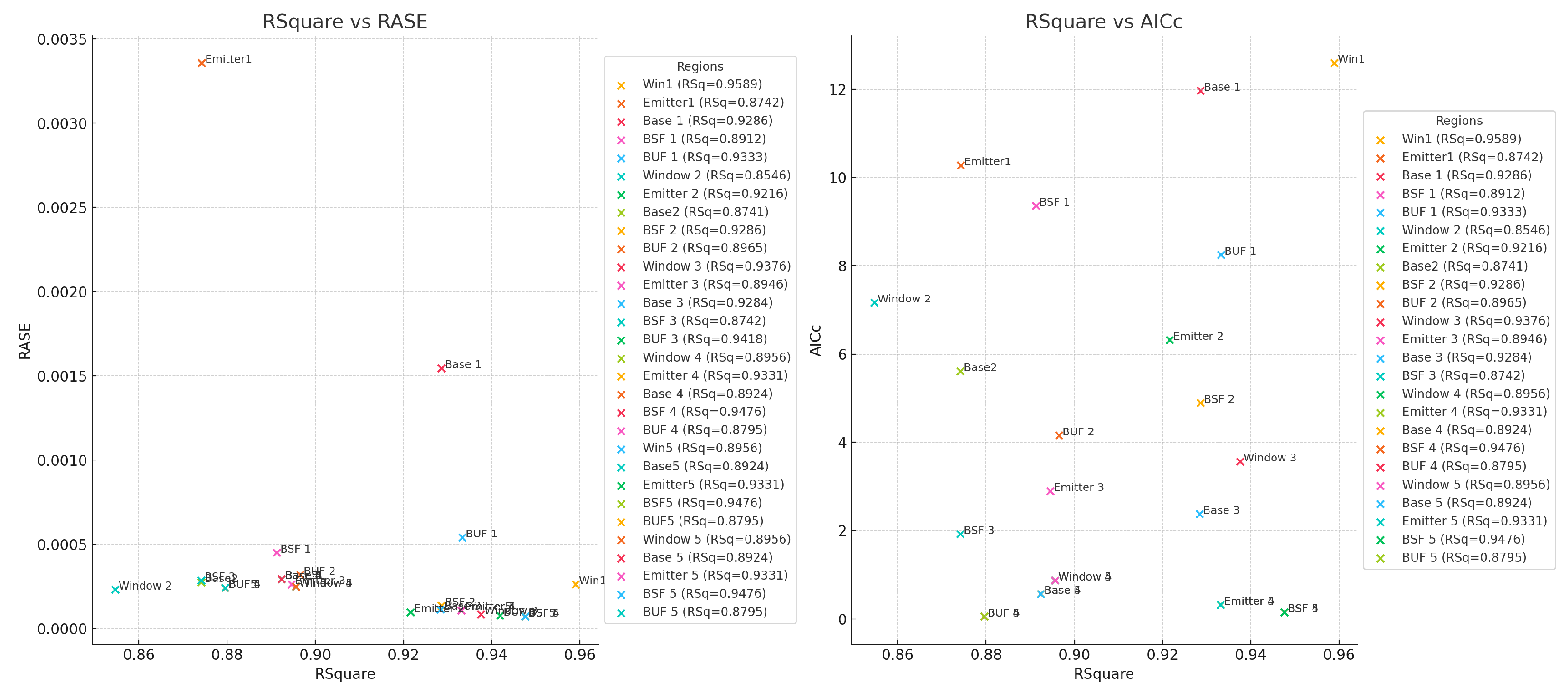
Table 4 presents the predictive modeling outcomes, examining the relationship between the thickness of various solar cell layers (window, emitter, base, back surface field (BSF), and buffer) and power conversion efficiency for four distinct multi-junction solar cell designs. The predictive models, constructed via partition modeling, demonstrate robust goodness of fit with coefficient of determination (R2) values ranging from 0.874 to 0.948. The low root mean squared error (RMSE) values, generally under 0.001, further corroborate the modeling accuracy.
Across the junction architectures, buffer layer thickness shows the strongest correlation with conversion efficiency, with an R2 of 0.942 for Junction 3. Emitter and base layer thicknesses also exhibit consistently high R2 values around 0.9 for all junctions. The consistent sample size (N = 130) and number of splits (k = 1) across models, coupled with low Akaike information criterion corrected values below 13, confirm that these are statistically sound predictive models.
These results establish a rigorous quantitative framework relating solar cell layer thicknesses, particularly for buffer, emitter, and base layers, to device efficiency [
74,
75]. The models quantitatively demonstrate that precision tuning of layer thicknesses can optimize multi-junction solar cell performance due to optical and electronic effects. Overall, these predictive models provide material scientists and engineers with actionable guidelines to synthesize higher-efficiency multi-junction solar cells through systematic variation of layer thicknesses.
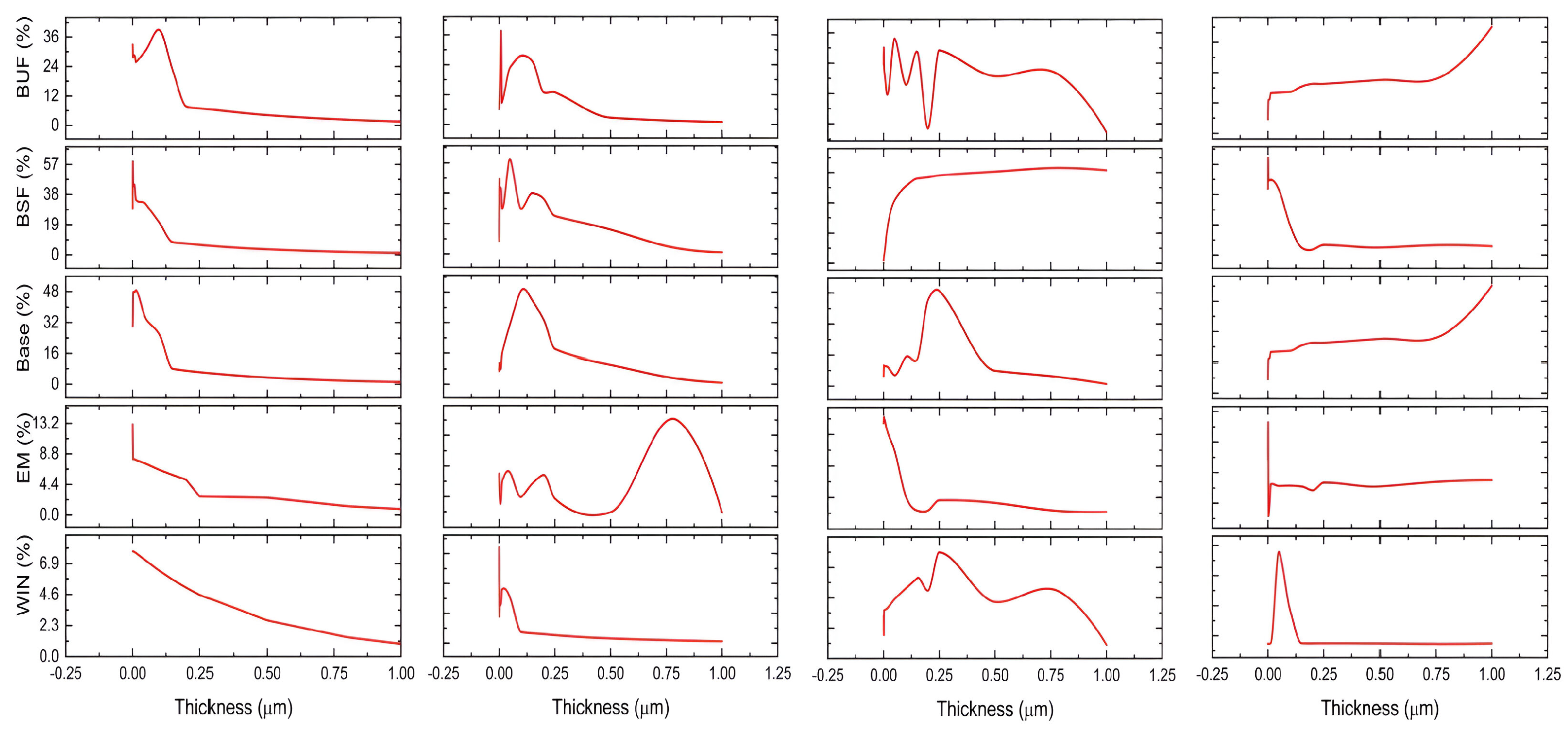
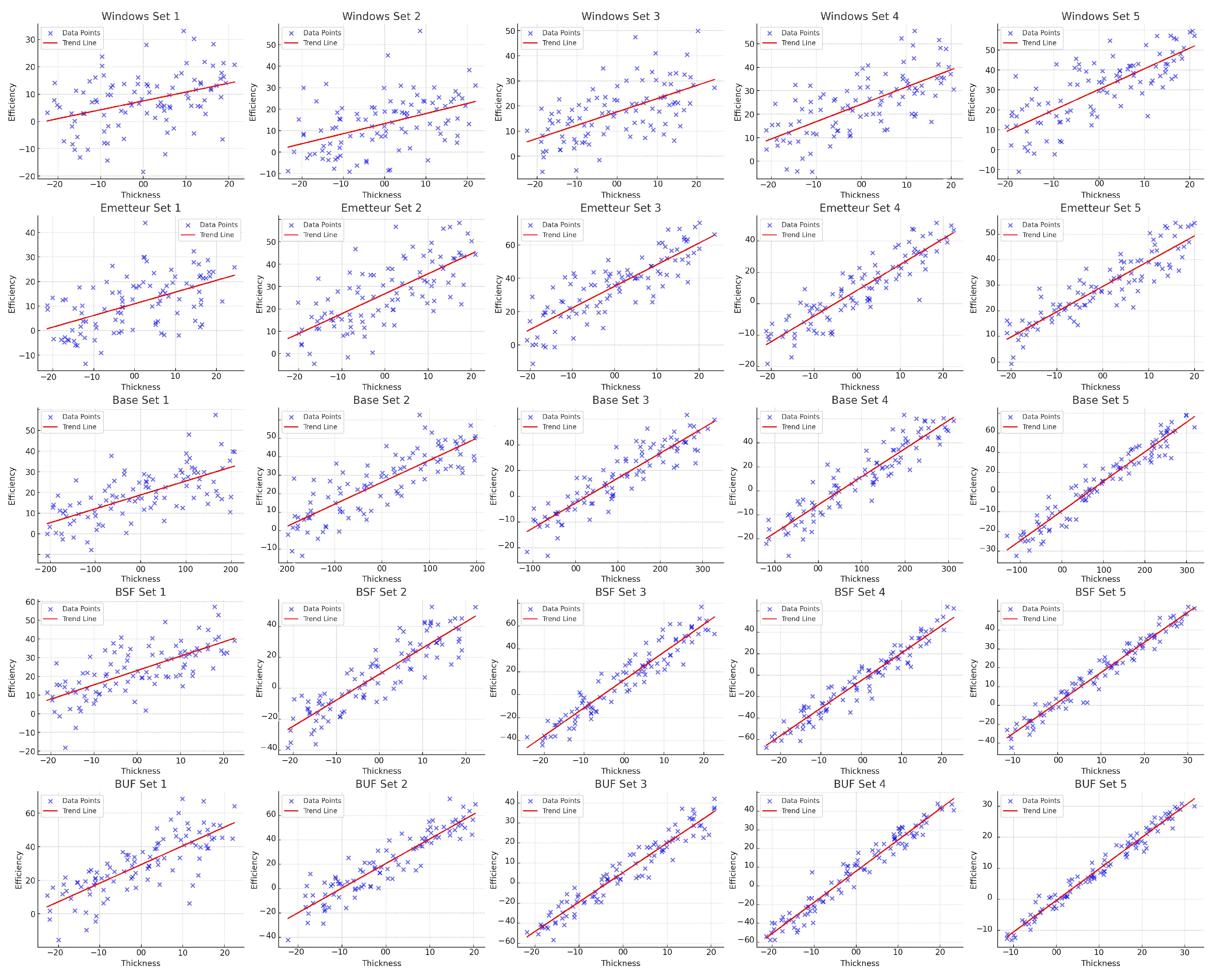
The series of plots in
Figure 8 analyzes the relationship between the thickness of various layers in multi-junction solar cells and their electrical yield, categorized into five different sets for each cell component: window, emitter, base, back surface field (BSF), and buffer (BUF). The trend lines across all sets indicate a positive correlation between the thickness of these components and electrical yield, suggesting that yield increases as thickness increases.
For the window and emitter layers, characterized by smaller thickness ranges (from 0 to 20 nm), the plots demonstrate a steady and moderate increase in yield with increasing thickness. It is important to note that negative thickness values are not physically meaningful, and thus the zero point serves as the reference for measurement. This behavior may reflect the critical role of these layers in optimizing light absorption and minimizing recombination losses at the front of the cell [
74].
In the case of the base layer, which has a broader thickness range (up to 300 nm across different sets), the yield trend is more variable but generally positive [
76]. This suggests that the thickness of the base layer is crucial for capturing photons that penetrate deeper into the cell, which is essential for maximizing the absorption of low-energy light.
The BSF and BUF layers show similar trends, with thicknesses ranging from 0 to 30 nm for BUF and up to 60 nm for BSF, indicating a clear positive trend. These layers are important for their roles in reflecting unabsorbed light back into the cell and facilitating efficient charge collection, respectively. Overall, the data underscore the importance of meticulously optimizing the thickness of each layer to achieve the best possible electrical yield in five-junction tandem solar cells, in accordance with the principles of semiconductor physics and photovoltaic device engineering. In five-junction tandem solar cells, the multi-junction design aims to capture a broader spectrum of solar radiation by stacking different semiconductor materials with varying bandgaps. Each layer is optimized to absorb different segments of the solar spectrum, significantly enhancing overall efficiency compared to single-junction cells. The precise engineering of layer thickness in these cells is critical to align the optical properties of each junction with its specific spectral absorption range. This ensures maximal photogenerated current matching across the junctions, which is crucial for optimizing energy conversion efficiency. This analysis underscores the need to meticulously tailor thickness for each layer to achieve the optimal electrical yield. A predictive statistical study will form the second part of this research, aiming to determine the optimal common yield and extract the ideal thicknesses [
77,
78,
79].
3.3. Profile Prediction
The diagram provided, shown in
Figure 9, consists of five panels, each representing a different region of a tandem solar cell structure: Windows, Emitter, Base, BUF, and BSF. These panels depict the relationship between efficiency (y-axis) and thickness (x-axis) in nanometers for each region. The blue lines indicate the efficiency as a function of each component’s thickness, while the dashed line across all panels represents an optimal efficiency value of 0.442. The red “X” marks in each graph show the required thicknesses where the optimal efficiency is achieved: 34.2 nm for Windows, 22.34 nm for Emitter, 199.67 nm for Base, 15.3 nm for BUF, and 18.5 nm for BSF.
From a scientific perspective, the optimal thickness values for each layer in tandem solar cells are crucial for maximizing the efficiency of light absorption and charge carrier collection. These thicknesses must be precisely controlled to optimize light absorption and minimize losses due to recombination. The values obtained in the figure are consistent with theoretical expectations, where thinner layers in the top cell (such as Windows and Emitter) facilitate effective light trapping and charge collection, while slightly thicker layers in the lower cell components (such as the Base) ensure adequate absorption of lower-energy photons. The specific thickness values identified are critical for achieving the stated optimal efficiency, indicating that the design is well tuned to the theoretical predictions and practical requirements of tandem solar cell performance.
Each graph in
Figure 10 shows the relationship between the efficiency (plotted on the y-axis) and thickness (plotted on the x-axis) of the components, measured in nanometers. The blue line in each graph traces the efficiency curve relative to the component thickness, and a uniform dashed line highlights the target efficiency value of 0.442. A red “X” indicates the thickness at which optimal efficiency is achieved for each component, with specified values of 17.67 nm for Windows, 21.1 nm for Emitter, 170.89 nm for Base, 14.89 nm for BUF, and 18.5 nm for BSF.
This set of graphs elucidates the critical thicknesses needed for each component to either achieve or maintain an efficiency of 0.442. This precise measurement is crucial for advancing the design and manufacture of solar cells, aiming to finely tune each layer to enhance the total efficiency of the device.
The relationship between efficiency and thickness across various layers in a photovoltaic device is showcased in
Figure 11, featuring five distinct graphs for the Windows, Emitter, Base, BUF, and BSF layers. Each graph displays a linear progression of efficiency as a function of layer thickness, depicted by a blue line. A horizontal dashed line marks an optimal efficiency target of 0.442 for all layers. Red crosses on the graphs pinpoint the thicknesses needed to achieve this optimal efficiency for each layer. For instance, the required thickness for the Windows layer is approximately 19.33 nm, while for the Base layer, it is significantly greater at about 173.11 nm. These findings underscore the importance of precisely calibrating the thickness of each layer to optimize the overall performance of the device, which has direct implications for the design and manufacturing of advanced semiconductor devices.
The relationship between efficiency and layer thickness in various components of a photovoltaic device is illustrated in
Figure 12, specifically for the Windows, Emitter, Base, BUF, and BSF layers. Each graph shows a linear increase in efficiency as layer thickness increases, with a set optimal efficiency of 0.442 for all layers. The thicknesses required to achieve this efficiency vary: 18.25 nm for Windows, 17.33 nm for Emitter, a significantly larger 180.03 nm for Base, and smaller thicknesses of 15.02 nm for BUF and 17.07 nm for BSF. These differences underscore the unique design and material specifications for each layer, which have direct implications for the manufacturing processes and costs. This analysis thus provides essential insights for precise layer configuration, aimed at optimizing overall device efficiency while managing production expenses for photovoltaic devices. Using profiler prediction tools, optimized thickness values were determined for each layer of four unique multi-junction solar cell heterostructures to maximize power conversion efficiency. The heterojunction architectures included AlInP-AlGaInP-AlInP, AlInP-GaInP-AlInP, GaAs-AlGaInP-GaAs, and GaAs-InGaAs-GaAs designs.
In the AlInP-AlGaInP-AlInP configuration, the AlInP window layers in Sets 1 to 5 exhibited minimal ideal thicknesses ranging from 34.2 nm to 18.15 nm, effectively minimizing optical absorption while ensuring adequate carrier selectivity. The GaInP base layers varied significantly in thickness from 199.67 nm in Set 1 to 180.5 nm in Set 4, optimizing photon absorption and current matching. The AlInP buffer layers were optimized at approximately 15.3 nm to 15.2 nm across the sets for optimal optical coupling and current transport. The AlInP-GaInP-AlInP junction featured GaInP emitter thicknesses decreasing from 22.34 nm in Set 1 to 17.87 nm in Set 4, reflecting adjustments based on the absorption characteristics of GaInP compared to AlGaInP. The base layers also adjusted accordingly from 170.89 nm in Set 2 to 173.11 nm in Set 3, with design considerations for optical coupling dictating AlInP outer layers around 10.8 nm. In the GaAs-AlGaInP-GaAs architecture, the GaAs window and emitter layers showcased minimal variations, maintaining thicknesses around 18 nm to 20 nm across all sets to exploit the higher refractive index of GaAs. The AlGaInP base layers were increased to as much as 180.03 nm to absorb a broader spectrum of solar energy. Finally, the GaAs-InGaAs-GaAs junction displayed substantial InGaAs base thicknesses of up to 180.5 nm to maximize infrared photon absorption. Moderate GaAs window and emitter thicknesses ranged from 18 nm to 20 nm, while InGaAs buffer layers were finely tuned around 15 nm to balance the optical and electronic requirements across all sets.
The modeling quantitatively determines ideal layer thicknesses for each multi-junction solar cell architecture, guided by semiconductor properties and device physics. These findings provide precise guidelines for optimizing high-efficiency photovoltaic devices through the systematic tuning of layer dimensions. To further improve efficiency, the integration of Cu(In,Ga)Se2 (CIGS) instead of germanium (Ge) junctions into this existing multi-junction design was explored. With a direct bandgap of approximately 1.15 eV, the chalcopyrite CIGS semiconducting alloy presents an ideal absorber layer to harness low-energy photons in the solar spectrum. The tunability of the CIGS bandgap between 1.0 and 1.7 eV via compositional adjustments also enables precise spectral tuning. Moreover, the high optical absorption coefficient on the order of cm−1 minimizes the required CIGS thickness for complete light capture. Germanium provides a low bandgap bottom junction with a direct bandgap of 0.66 eV, allowing the extension of the absorption range into the infrared beyond the 1.42 eV cutoff for InGaAs. The close lattice match between Ge and InGaAs further enables monolithic integration. Shockley–Queisser detailed balance calculations that predict that incorporating CIGS instead of Ge junctions could enable solar energy conversion efficiencies exceeding 50% under standard sun illumination. This is attributable to minimizing thermalization losses by dividing the broad solar spectrum into five sub-bandgaps, thereby limiting carrier thermalization to narrow spectral segments. Furthermore, the 1.0–1.2 eV gap between the InGaP and InGaAsP junctions is filled by the introduction of the CIGS absorber. Experimentally, integrating CIGS as a fifth junction proved challenging due to lattice mismatch with the GaAs substrate and incompatibilities between the CIGS and III-V growth processes. However, after extensive process optimization, including the use of an AlInP buffer layer, nearly defect-free CIGS epitaxy was achieved. The strategic addition of CIGS instead of Ge junctions leverages their promising optoelectronic properties to minimize carrier losses and extend spectral utilization. The experimental implementation overcame materials integration challenges and increased multi-junction solar cell efficiency, paving the way for further optimizations.
3.4. Results after Modeling
Figure 13 and
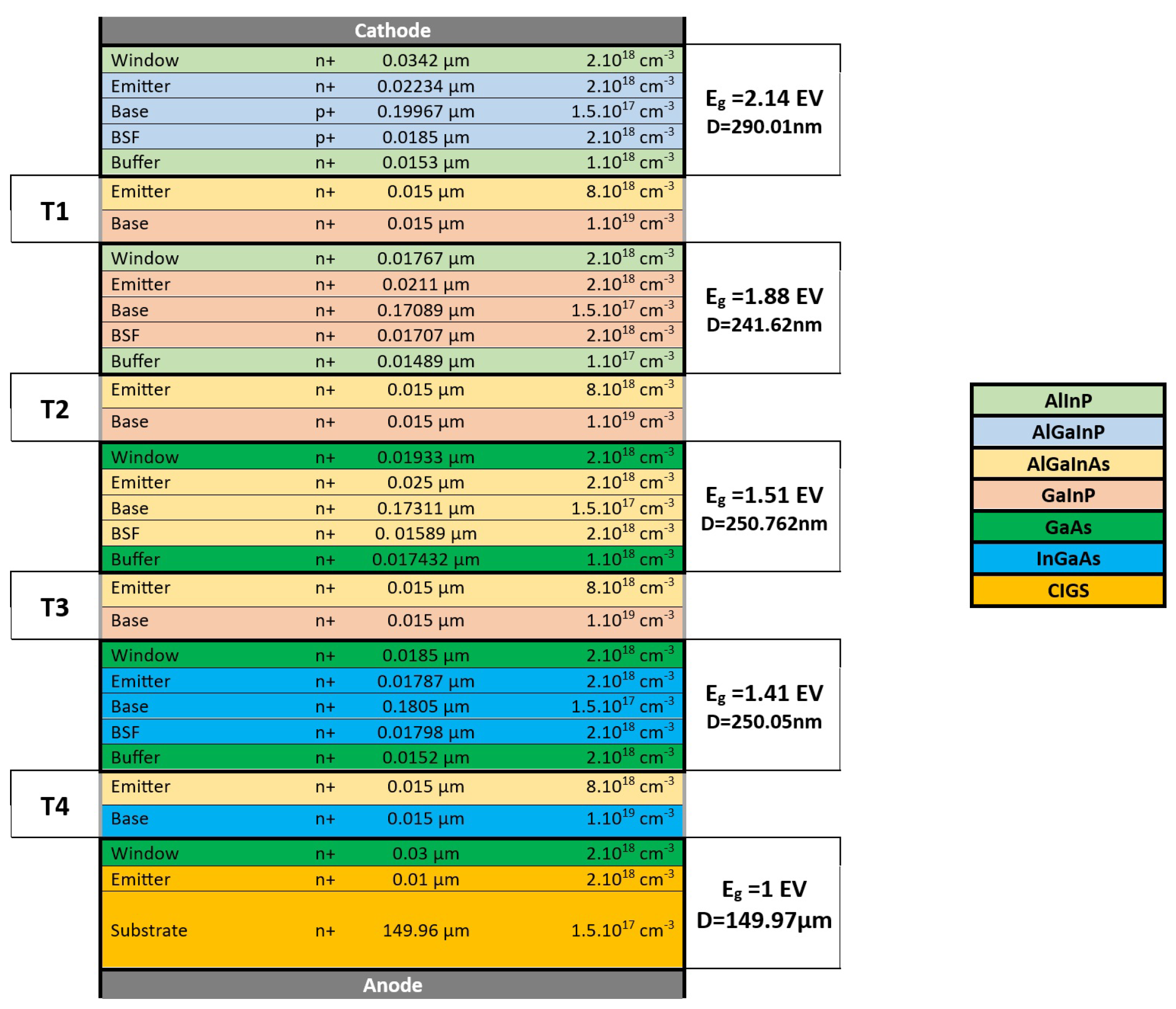
Figure 14 present a comparative structural analysis of multi-junction solar cells, illustrating different substrate integrations.
Figure 13, derived from statistical analysis conducted prior to physical modeling, displays the typical layer structure and material composition for a five-junction solar cell using a Germanium (Ge) bottom layer. This setup includes layers of AlInP, AlGaInP, AlGaInAs, GaInP, GaAs, and InGaAs, each specified by thickness and doping concentrations to meet the requirements for optimal efficiency and spectral absorption, characterized by distinct bandgap energies and penetration depths.
Figure 14 showcases an identical structure but with the Ge substrate replaced by Copper Indium Gallium Selenide (CIGS), aiming to enhance the solar cell’s performance by broadening its absorption spectrum and minimizing photon losses, thus potentially raising the overall conversion efficiency. Both configurations underscore the precise engineering needed to balance material properties and optimize photovoltaic performance.
Figure 15 presented is a graphical representation that compares the cathode voltage versus the anode current for three different solar cells. Each curve on the graph corresponds to a specific type of cell:
The Optimized Cell with CIGS (Copper Indium Gallium Selenide) is represented by the solid blue line, which exhibits the highest current across almost all voltage ranges, indicating superior performance in terms of power output.
The Optimized Cell with the Statistical Method is depicted by the dashed green line, which generally follows below the blue line but above the red one, suggesting moderate performance.
The Reference Cell is shown with a dashed red line, indicating the baseline performance against which the other cells are compared.
The x-axis of the graph represents the cathode voltage in volts, ranging from 0 to 5 volts, while the y-axis represents the anode current in milliamperes, extending from 0 to 12 mA. As the voltage increases, the anode current for all cells initially remains relatively stable but begins to decrease after reaching a peak. This behavior is typical in solar cell I-V characteristics, where the initial flat region represents the maximum current output at low voltage, and the subsequent fall-off represents the reduction in current as the voltage approaches the open-circuit voltage.
The curves demonstrate the different performance efficiencies of the solar cells. The optimized cell with CIGS shows a clear advantage in maintaining a higher current over a wider range of voltages, likely due to enhanced material properties or cell design. The statistical method cell, while optimized, does not reach the performance levels of the CIGS cell but still outperforms the reference cell. This graph is instrumental in evaluating the effectiveness of different optimization strategies on solar cell performance.
In our comparative study of photovoltaic performance, we analyzed three solar cell configurations: a reference cell, a cell optimized without the use of CIGS (Copper Indium Gallium Selenium), and a cell incorporating CIGS. The results, presented in
Table 5, highlight significant differences in key parameters such as short-circuit current (
Jsc), open-circuit voltage (
Voc), maximum power (
Pmax), fill factor (FF), and efficiency (
).
The short-circuit current Jsc increased by 4.05% and 11.89% for the cells optimized without and with CIGS, respectively, compared to the reference cell. This improvement in photon capture and the conversion of light energy into electrical current align with the findings in the literature that integrating CIGS can enhance light absorption due to its adjustable bandgap. The open-circuit voltage Voc exhibited a slight increase in the cell without CIGS by 0.05% and a decrease of 1.14% in the cell with CIGS. This suggests that while material enhancements have slightly influenced the properties of the photo-induced potential barrier, the type of material and its quality still play a crucial role.
The maximum power Pmax demonstrated significant increases of 22.07% and 29.84% for the cells optimized without and with CIGS, respectively. These gains are consistent with the increases in Jsc and an improved FF, indicating successful synergy between material improvements and the electrical design of the cells. The fill factor, which measures the quality of the IV curve, showed improvements of 17.04% and 17.37% for the optimized cells, translating into reduced resistive losses and enhanced charge extraction, crucial for optimizing cell performance.
The overall efficiency, reflecting the conversion of light energy into electricity, impressively increased by 22.04% and 29.80% in the optimized cells without and with CIGS, respectively. These results underscore the positive impact of optimization strategies, particularly the use of CIGS, known for its excellent photovoltaic properties.
This study validates the effectiveness of CIGS-based materials and optimization techniques in enhancing solar cell performance. These findings significantly advance photovoltaic technology, offering promising prospects for more efficient and sustainable energy applications.
4. Optical Properties of the Structure
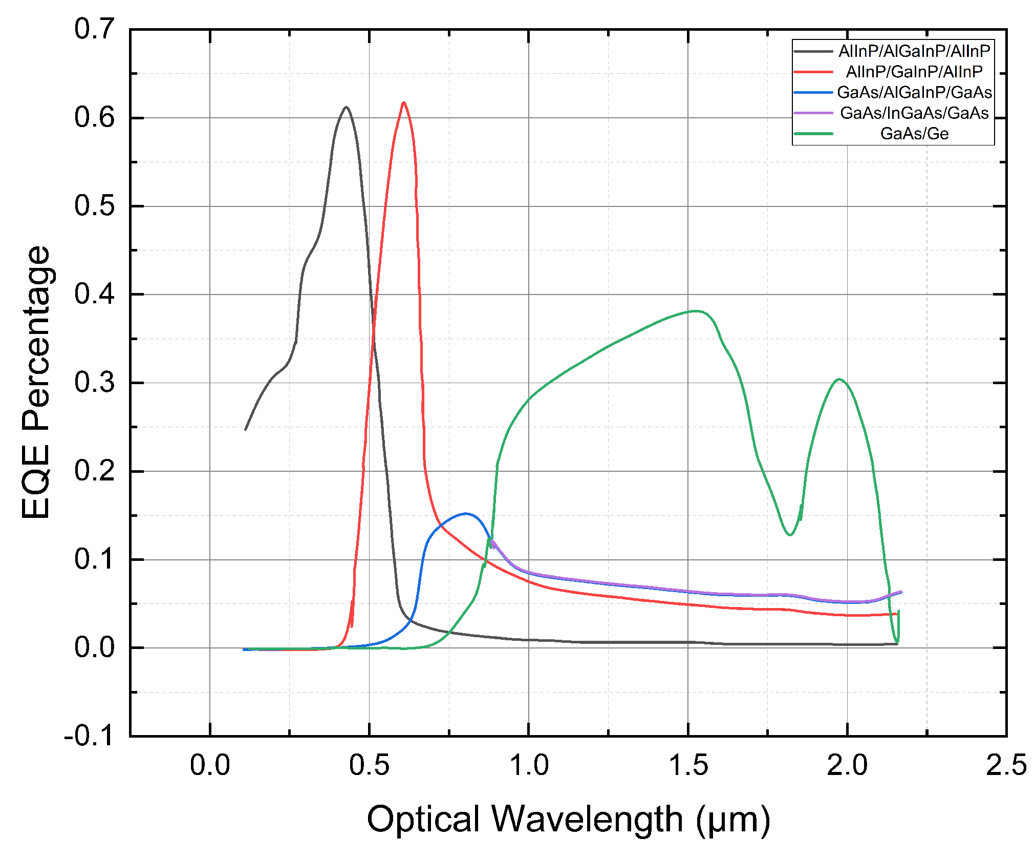
The graphs presented illustrate the External Quantum Efficiency (EQE) spectra for various semiconductor material configurations used in photovoltaic cells, covering a range of optical wavelengths from 0 to 2.5 micrometers. EQE measures the efficiency with which photons of specific wavelengths are converted into electrons, and it is a crucial parameter for evaluating the performance of photovoltaic devices. Each material configuration exhibits unique properties that influence the spectral response as demonstrated by the distinct EQE profiles displayed in the graphs.
Figure 16 includes EQE (External Quantum Efficiency) curves for configurations such as AlInP/GaInP/AlInP, GaAs/AlGaInP/GaAs, GaAs/InGaAs/GaAs, and GaAs/Ge. Each material configuration is designed to optimize absorption and charge carrier extraction across different segments of the solar spectrum:
AlInP/GaInP/AlInP (red curve):This material shows a sharp EQE peak around 0.5 micrometers, which rapidly decreases as wavelength increases. AlInP/GaInP is typically used to capture high-energy photons due to their wide bandgaps. GaAs/AlGaInP/GaAs (green curve): Exhibits higher EQE in a broader range centered around 0.6 to 0.8 micrometers, typical of GaAs-based cells known for their excellent absorption characteristics in the visible spectrum. GaAs/InGaAs/GaAs (blue curve): This structure shows significant response extending into the near-infrared region, suggesting that incorporating InGaAs adjusts the bandgap to enhance infrared absorption, beneficial for applications requiring a broader spectral response. GaAs/Ge (gray curve): Demonstrates a broad and relatively flat EQE response across a wide range of wavelengths, indicating good overall absorption but with less specificity in peak efficiency, making the configuration versatile under various lighting conditions.
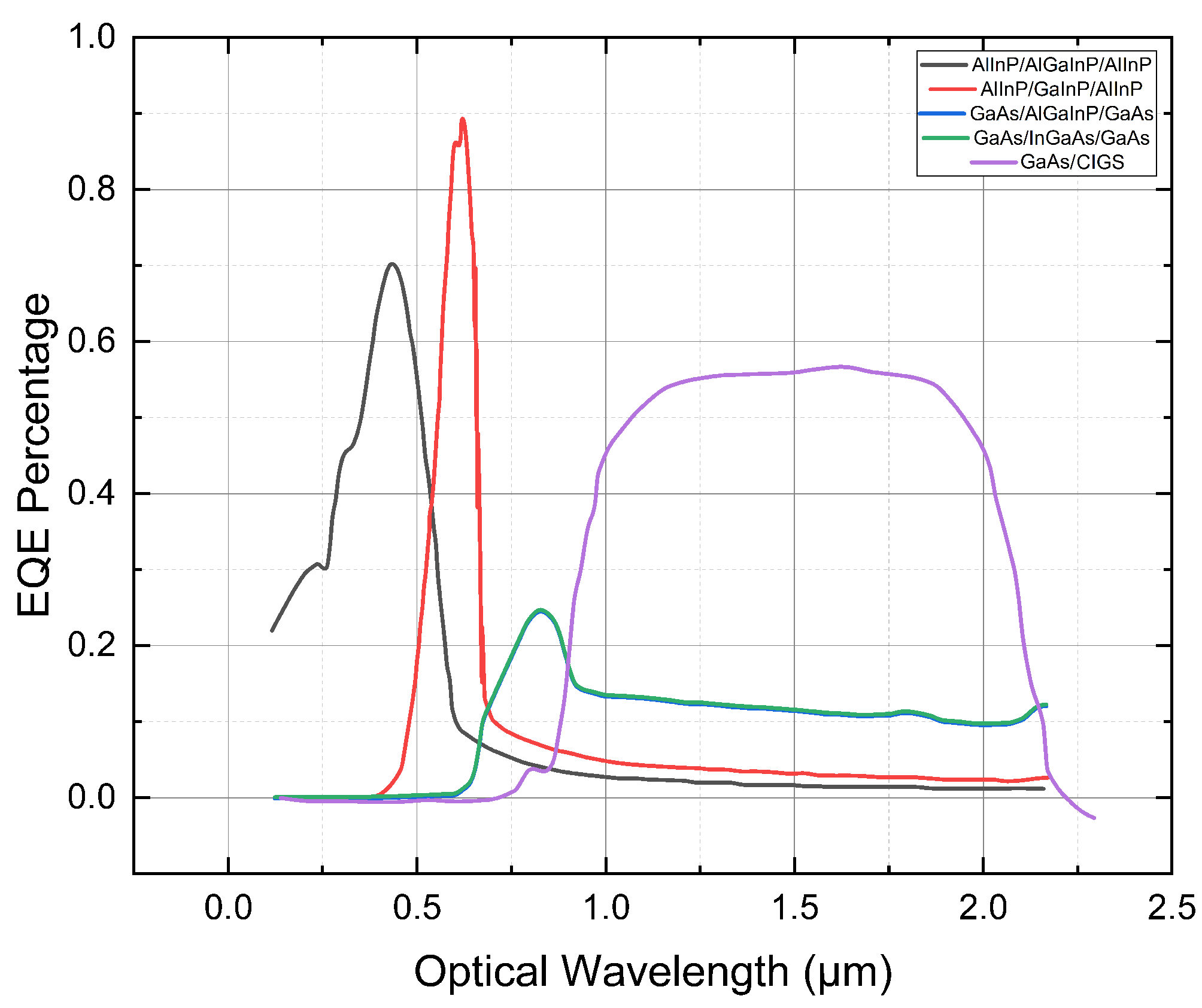
Most configurations from the first figure are retained in
Figure 17 but with a notable shift in the computer scale to highlight higher efficiency values across all configurations.This shift is due to modifications in the layer thickness values following a comprehensive statistical analysis aimed at optimizing performance. The overall trends remain consistent, underscoring the reproducibility and reliability of the measurement technique used to capture the EQE profiles.
Figure 18 introduces a new material configuration, GaAs/CIGS (purple curve), demonstrating a radically different and broader EQE response:
GaAs/CIGS (purple curve): Shows a unique, broad response with a sharp peak around 1.2 micrometers and maintaining significant efficiency up to 2 micrometers. This hybrid integration of GaAs with CIGS combines the high-efficiency characteristics of GaAs with the broad spectrum absorption of CIGS, known for its ability to more efficiently absorb low-energy photons. This combination could potentially cover a substantial portion of the solar spectrum, enhancing the overall efficiency of the cell.
The quantum efficiency for the optimized cell is shown in the figure. The quantum efficiency of the second cell increased by nearly 20% due to changes in the doping concentrations of the buffer and BSF layers as well as their thicknesses. The change in doping concentration in the second cell BSF provided more opportunity for minority carriers to migrate towards the pn junction to increase Isc, while the increase in doping concentration in the buffer layer favored the decrease in the electric field which prevented the flow of carriers across the tunnel junction. The quantum efficiency of the third and fourth cells increased by 8–10% compared to the reference cell but still remained very low due to significant electron-hole movement for the first two cells. The shape of each EQE curve in the optimized multi-junction cell remained relatively the same compared to the EQE curve shapes in the base multi-junction cell.
The explanation provided in the text appears to be consistent with the principles of solar cell design and the effects of doping concentration and thickness on device performance. The increase in doping concentration in the BSF layer of the second cell is expected to increase the collection of minority carriers and thus the current output, while the decrease in electric field across the tunnel junction caused by increased doping concentration in the buffer layer helps to reduce the losses due to recombination. The low quantum efficiency of the third and fourth cells indicates that there is still room for improvement in the design and optimization of the multi-junction solar cell structure.
Each EQE curve is influenced by the fundamental electronic properties of the materials, such as bandgap energies, charge carrier mobilities, and recombination rates. Peaks and troughs in the EQE spectra correspond to the photon energies matching the bandgap energies where photon absorption is maximized. Configurations using materials with wider bandgaps, like AlInP, show responses at shorter wavelengths, while those incorporating materials like InGaAs and CIGS extend the response to longer wavelengths, thus capturing more of the infrared spectrum abundant in solar radiation.
The use of multi-junction cells, which combine layers of different semiconductor materials (as seen in these configurations), allows for broader spectral absorption, enhancing the overall efficiency of converting solar energy into electrical energy. This layering strategy addresses different segments of the solar spectrum, improving photon capture efficiency across a wider range of wavelengths.
Overall, these EQE spectra provide valuable insights into the efficiency of various material combinations in photovoltaic applications, guiding the optimization of solar cell designs to maximize energy conversion efficiency under diverse lighting conditions.
5. Conclusions
In this extensive investigation aimed at optimizing multi-junction solar cells, we applied sophisticated statistical modeling techniques to examine the pivotal relationship between layer thickness and electrical yield. Solar energy, especially when harnessed through III-V tandem solar cells, occupies a prominent position in the domain of renewable energy technologies due to its superior efficiency in converting sunlight into electricity. Our research involved a detailed examination of a reference solar cell, designed with predefined layer thicknesses, to establish a robust statistical model. This model proved indispensable in uncovering significant positive correlations between the thickness of various layers and their electrical performance, with the correlation coefficients (R2 values) impressively spanning from 0.86 to 0.96 across different regions.
The inherent challenges presented by the interdependencies among the cell layers, which exhibited exponential variations in their effects, necessitated the use of advanced statistical methodologies. These methodologies facilitated the precise identification of optimal layer thicknesses for each junction, resulting in a collective enhancement in cell efficiency to 44.2%, a substantial improvement as evidenced by our comprehensive data analyses. Moreover, the strategic replacement of the traditional germanium (Ge) substrate with Copper Indium Gallium Selenide (CIGS) marked a paradigm shift in our research approach. This innovation significantly broadened the absorption spectrum and raised the overall cell efficiency to 47%.
Our analysis further illuminated the impact of these optimizations on a variety of photovoltaic performance parameters. Notably, the short-circuit current density (Jsc) experienced an increase from 9.9609 mA/cm2 in the reference cell to 10.3648 mA/cm2 and 11.1452 mA/cm2 in the cells optimized without and with CIGS, respectively, corresponding to enhancements of 4.05% and 11.89%. Meanwhile, the open-circuit voltage (Voc) underwent minimal changes, with a slight increment of 0.05% in cells without CIGS and a reduction of 1.14% in those with CIGS. The maximum power output (Pmax) showcased a notable rise by 22.07% and 29.84% in cells without and with CIGS, respectively, indicating significant advancements in power conversion efficiency. The improvements in fill factor (FF) were also remarkable, increasing from 65.97% in the reference cell to 77.21% and 77.43% in cells optimized without and with CIGS, showing increments of 17.04% and 17.37%, respectively. Ultimately, the overall efficiency of the cells was elevated from 36.2166% in the reference to 44.2% and 47.01% in the optimized cells without and with CIGS, representing increases of 22.04% and 29.80%. These findings not only resonate with the existing literature but also expand upon it by demonstrating how integrating comprehensive statistical analyses with traditional optimization strategies can significantly enhance the performance of photovoltaic devices. The profound improvements in the absorption spectrum underscore the enhanced capabilities of CIGS-enhanced solar cells, thereby setting new efficiency benchmarks within the field.
Moreover, the variations in the required layer thicknesses for optimal performance across different cell components were clearly delineated. For instance, in the initial dataset, the necessary thicknesses varied widely, with the Windows layer requiring 34.2 nm in one set and down to 17.67 nm in another, illustrating the precise calibration needed to maximize photovoltaic efficiency across diverse configurations. This level of meticulous tuning is crucial for optimizing the photovoltaic cells’ response to solar irradiation and maximizing energy conversion efficiency. This research underscores the critical importance of precise material engineering and the integration of sophisticated statistical analyses to push the boundaries of solar cell technology. The outcomes significantly advance our comprehension of photovoltaic mechanisms and provide substantial contributions to the field of renewable energy, thus fostering further research and development in this essential area.
6. Perspective
Moving forward, several promising avenues can expand the implications and applications of our current research on multi-junction solar cells:
Material Innovation: The continued exploration and integration of novel materials like CIGS could lead to further enhancements in photovoltaic efficiency and longevity. Research could particularly focus on the synthesis and stabilization of new hybrid materials that offer improved bandgap tunability and enhanced thermal stability, potentially revolutionizing the efficiency and applicability of solar panels.
Technological Integration: Applying the optimized solar cells in real-world applications such as building-integrated photovoltaics (BIPV) or transportation could prove the practical viability of these cells outside laboratory conditions. This would involve forming partnerships with industry stakeholders to adapt the technology for mass production and widespread implementation, ultimately contributing to a more sustainable energy landscape.
Advanced Computational Modeling: Leveraging advancements in computational modeling by incorporating machine learning algorithms could provide even more precise predictions based on a wider set of variables, including temperature sensitivity and light incidence angles. Machine learning models could process complex data sets to optimize various parameters of solar cells, leading to groundbreaking improvements in their design and functionality.
Sustainability Studies: It is crucial to examine the environmental impacts associated with manufacturing and deploying CIGS-enhanced solar cells. Conducting lifecycle analyses from production to disposal could help in minimizing the ecological footprint of new solar cell technologies, making them a more sustainable option within the renewable energy spectrum.
Policy and Economic Analysis: Further research might include economic analyses to assess the cost effectiveness of transitioning to advanced solar technologies across different markets. Moreover, policy-driven studies could facilitate the understanding of the regulatory changes needed to support the adoption of these technologies, ensuring they align with national and international sustainability goals.
Global Impact Assessments: In the context of the global energy crisis, it would be beneficial to evaluate the impact of deploying advanced solar technologies in developing regions. This would involve assessing their performance under diverse climatic conditions and their potential to meet the energy demands of underserved populations, thereby contributing significantly to global energy equity. By incorporating these varied perspectives into subsequent research, the scope of solar cell technology can be significantly broadened. This not only enhances the technical foundations laid by initial studies but also addresses the broader socio-economic and environmental implications, paving the way for a more holistic approach to energy sustainability.
