1. Introduction
In an electrical vehicle, the control over the inverter can be lost due to various factors. In such cases, the control must ensure the provision of a fail-safe state. Two different control strategies are conceivable. On the one hand all switches can be turned-off [
1]. This will lead to an excessive voltage at the DC-link capacitor, semiconductors and leads to a uncontrolled feed back into the battery. On the other hand an active short circuit (ASC) can be applied [
2], which prevents the voltage rise and feed back into the battery [
3]. Therefore, the machine is shortened by either turning all high-side switches (HSS) or low-side switches (LSS) on [
2]. During the active short circuit (ASC) state, the current is typically two up to four times higher than in normal operation [
4,
5,
6,
7] and hence is a surge current operation. This can be observed in
Figure 1. Consequently, the semiconductor must be capable of withstanding the surge current of the active short circuit (ASC).
This paper presents a comparative analysis of the surge current robustness of different semiconductors with respect to ASC. Two different measures are used to quantify the surge current robustness. The first one evaluates the robustness of the semiconductor with respect to its die area. The second one relates the robustness to the nominal current of the module. This approach evaluates the surge current robustness with respect to the application and represents an overload capability. For the rated current, a virtual module is designed for all devices. Therefore, the static and switching behavior is measured for all devices under the same conditions.
A minimum of six series of surge current measurements are performed on all devices. The series will vary in pulse duration and case temperature . The goal is to predict the surge current robustness under any ASC condition. Therefore, the measurements will be used to define a safe operating area criterion. A loss model is also derived from the measurements. Since the losses of a semiconductor are typically temperature dependent, the junction temperature is calculated during the evaluation. The method of defining a safe operating area for SiC and GaN devices is explained using the example of the GaN dMode. The modeling and SOA criterion for the Si IGBT and Si diode are also presented. Then the characteristics of each device are shown. Finally, the surge current robustness will be compared as described before.
Investigations into surge currents have already been conducted with a variety of semiconductors, including Si [
8,
9,
10], SiC [
8,
9,
11,
12,
13], and GaN [
14,
15]. However, the investigations are in the reverse direction, with a diode, body-diode, and a closed channel of the active device. The present paper focuses on ASC, where the channel is always open. Accordingly, the channel is open in both the forward and reverse directions during the surge current.
Figure 1 depicts a representative ASC waveform for a typical machine utilized in electrical vehicles. As outlined in [
5,
16,
17], the ASC current can be conceptualized as a combination of a static sinusoidal current and a decaying DC offset. The specific current waveform is dependent upon the machine, frequency, and current, as well as the rotor position at the time of ASC activation. The papers [
2,
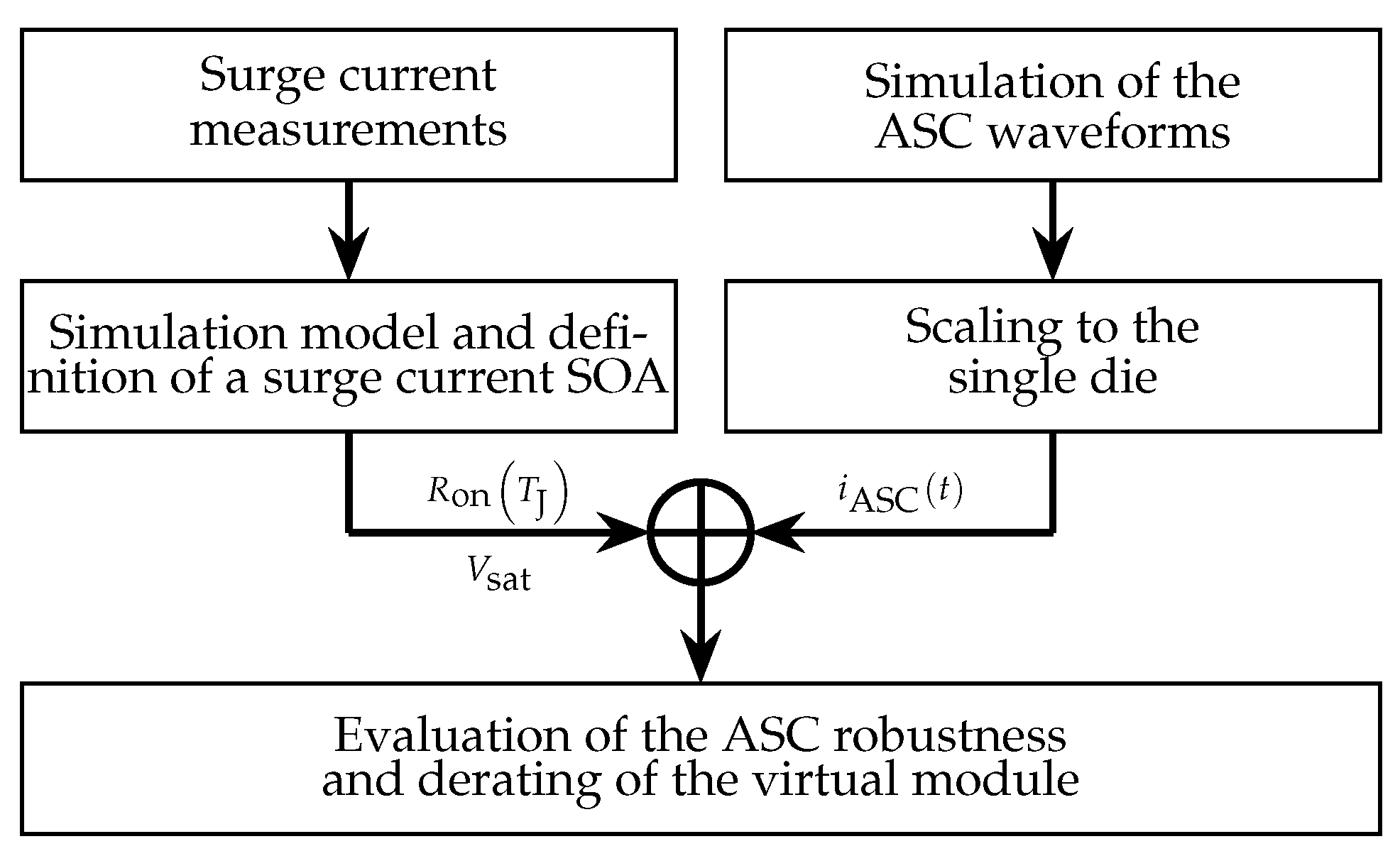
17] emulate a single active surge current waveform. However, this does not represent all possible waveforms. In this paper, as well as in the paper [
18], surge current measurements are performed, a SOA criterion is defined, and a loss model is established, as depicted in
Figure 2. As a result, any active short circuit waveform can be evaluated through simulation.
The present study focuses on semiconductor devices with a voltage rating of 650 to 1.2 kV, which are commonly utilized in the drive inverters of electric vehicles. As previously demonstrated in [
2], the robustness of the ASC has been investigated for Si, while [
2,
17,
19] have done the same for SiC.
2. Design of the Virtual Modules
The devices under consideration are single dies. For drive applications, multiple single dies are placed in parallel in a half-bridge configuration within a power module. In this evaluation, we assess the same module environment for all devices in our single die measurements, thermal and loss calculations, which are utilized to design a virtual B6 module (similar to [
20]). The current density of each device is than given, which reference to the current density in the virtual module. Therefore the conduction losses are modeled based on curve tracer measurements. The switching losses are characterized in double pulse measurements. The stray inductance of the double pulse measurements, conducted with single dies, is scaled to the stray inductance of the virtual module [
21].
Table 1 lists the parameter of the virtual module. For all devices there is a constant stray inductance current product, which ensures, that the stray inductance environment is similar. The switching losses are measured for all devices. The thermal environment of the virtual module is also defined as constant. This is ensured by a area specific thermal resistance. For all devices the maximum allowed junction temperature
is set to 25 °C below the maximum specified in the datasheet
. The fluid temperature of the coolant is set to 65 °C.
For the 650 to 750 V devices the DC-link voltage is set to 400 V. For the 1.2 kV devices the DC-link voltage is 800 V. The maximum allowed over-voltage for the 400 V DC-link devices is approximately 200 V and 250 V for the 800 V DC-link voltage devices.
Table 2 shows the nominal current of the different devices under the conditions of the virtual module. For the SiC JFET [
22] as well as for the GaN eMode [
23,
24] and GaN dMode a Miller clamping [
25,
26,
27,
28] is necessary to prevent or limit the influence of the parasitic turn on (PTO). The given current density for these three devices is only achievable with the proposed Miller clamping.
3. Measurement Setup and Junction Temperature Calculation
Figure 3 depicts the surge current measurement circuit. In the initial stage, the capacitance
C is charged. Consequently, the IGBT A is activated. Prior to the surge current pulse, the IGBT A is deactivated. Subsequently, the IGBT B is activated. At this point, the current begins to rise through the inductance
L, exhibiting a nearly sinusoidal waveform. Subsequently, the IGBT B is deactivated once more after one half-wave period. The device under test (DUT) is maintained in the on state throughout the duration of the experiment.
Figure 4 shows the measurement setup with the Si IGBT. All voltages are measured with low voltage passive probes. The current is measured with a current transducer (LEM HTA 200…1000-S) based on the Hall effect with a bandwidth of 50 kHz, which is adequate for pulse widths in the millisecond range. The current steepness is therefore limited by the inductance
L. For high temperature measurements, a copper bar with a heating resistor is placed on the device. The temperature of the copper bar is controlled with a two point controller. It should be noted that the capacitor
C is positioned below the table and, as a consequence, is not visible in
Figure 4.
A minimum of six measurement series have been perfomed on all devices. The specific conditions of the measurement series, including the temperature of the device and the duration of the pulse, vary. Two temperature levels were considered: 25 °C and 125 °C.
Table 3 lists the capacitor and inductor combinations for the various pulse durations. Given the values of the inductor (
L) and capacitor (
C), the duration of the pulse can be calculated using the following Equation:
Given a voltage step of 1 V, the minimum resolution
R of the peak current values can be calculated as follows:
For each measurement series the maximum current is increased incrementally until a defect is observed. Each pulse is stored for subsequent use in the validation of the loss model and SOA criterion. Subsequently, the last good pulse (LGP) is employed as an indicator of the surge current robustness, whereas the first bad pulse (FBP) is utilized to assess the defect mechanism.
Figure 5 depicts a Foster model comprising four links. In order to evaluate the surge current pulses, it is necessary to ascertain the junction temperature. Consequently, the junction temperature is calculated based on the measured drain current and drain-source voltage. The product of the current and voltage represents the losses
. The losses will be incorporated into the Foster model, which calculates the temperature rise between the case
and the junction. The Foster model is performed with four up to six links.
The Foster can be derived out of the thermal impedance curve, which is mostly given in the datasheet. The Foster link coefficients
and
have to be fitted according [
35]. If the thermal model is given as a Cauer model it can be transformed in a Foster network according [
36].
Figure 6 depicts the selected surge current pulses for the 9.5 ms measurement series at 25 °C case temperature of the GaN dMode. As illustrated in the upper portion of
Figure 6, the surge current is depicted. As previously stated, the current is approximately sinusoidal with a half-wave symmetry. The middle part of the
Figure 6 depicts the voltage curves. There is a notable rise in voltage from the last good pulse (LGP) to the first bad pulse (FBP), in which the defect occurs. As shown in the lower part of the
Figure 6, this is accompanied by a significant increase in temperature. Subsequently, a criterion for the SOA under surge current conditions will be defined, along with a loss model that incorporates current saturation.
4. Safe Operating Area and Modeling
4.1. Safe Operating Area Criterion
As illustrated in
Figure 6, the GaN dMode exhibits a current saturation during surge current pulses. The transition from the linear to the saturation region can be defined by the saturation voltage, which can be expressed as follows:
Equation (
3) defines the saturation voltage as the difference between the positive driving voltage
and the threshold voltage
. The driving voltage can be either the nominal driving voltage or a voltage applied by a special driver for the ASC. The threshold voltage can scatter from device to device. Futhermore the threshold voltage is also a function of the junction temperature. The influence on the GaN devices on the threshold voltage is rather small.
Figure 7 depicts the voltage current density characteristics of six measurement series. Therefore the maximum drain-source voltage of each surge current pulse is plotted as a function of the maximum drain current density in the same pulse. Furthermore the minimum, typical and maximum saturation voltage is plotted. One can observe that the voltage rises strongly above the saturation voltage. This effect is especially strong for the 9.5 and 45 ms pulse duration.
Figure 8 depicts the comparison of the LGP current density values with the current density at the saturation criterion. It shows that for the most conditions the current density at the saturation criterion is about 63 to 89 % of the LGP value. This indicates that for the design of the module the saturation is a valid SOA criterion.
4.2. Loss Model
For the loss model the on-state resistance is modeled. There are two different approaches for the on-resistance model. For both approaches the on-resistance is modeled temperature dependent. In contrast to the second approach, the first approach do not take the current saturation into account.
Equation (
4) defines the on-state resistance model without current saturation. The resistance is thereby modeled as a second order polynomial.
Equation (
5) defines the on-state resistance model with current saturation. The current saturation is therefore modeled with a exponential function. The coefficients
a,
b and
c are modeled with a first or second order polynomial.
Figure 9 depicts the fitting of the two different on-state models out of static device analyser measurements. On the left side the model without current saturation is shown. The on-resistance is evaluated at 0 A drain current. This model is only valid until the saturation voltage is reached. On the right side the on-resistance is modeled as a function of the drain current for each measured temperature. It can be observed that for both models the fitting quality is high.
Figure 10 depicts two different surge current pulses with the measured and simulated waveforms for the 9.5 ms pulse duration and 25 °C case temperature measurement series. On the left side the last pulse below the saturation voltage of the measurement series is shown. For both models the drain-source voltage and hence the junction temperature is in good agreement. On the right side the LGP is shown. The on-state resistance model without the current saturation underestimates the losses. The second model with current saturation instead exhibit a high accordance with the measured drain-source voltage as well as the junction temperature.
In the following the characteristics of the different devices during surge currents will be shown as well as the SOA criterion and the loss model. Also a defect temperature range and a defect mechanism will be given.
4.3. Dynamic On-Resistance of GaN HEMTs
The effects of GaN trapping continue to exert an influence on the device’s behavior. A considerable body of literature addresses the trapping mechanisms [
37], methods to prevent it [
37], the characterization thereof [
38] and characterizations with stable charge trapping states [
39]. The traps are predominantly filled during the blocking of the high drain-source voltage [
40] and due to hot electrons during the switching transitions [
41]. In the surge current measurements, the devices are maintained in a constantly turned-on state. In this state, the traps are typically depleted [
40]. The following section will analyze the surge current measurements in order to identify any potential instances of the dynamic on-resistance.
Figure 11 depicts the measured and simulated waveforms of the loss model without saturation. The waveforms on the left side are presented for three distinct peak current values. It can be observed that there is a high degree of correlation between the drain-source voltage and the junction temperature of the measurements and simulation. The maximum values of the drain-source voltage
and the junction temperature
of the entire measurement series are illustrated on the right side of
Figure 11 as absolute and relative values. It can be observed that the discrepancy between the simulated and measured drain-source voltage for high current densities is below 2.5 %. Therefore, the difference is indistinguishable from the measurement error. Consequently, the model of the static measurements aligns with every surge current pulse, and there is no evidence of the dynamic on-resistance.
In this evaluation, the influence of the dynamic on-resistance can be disregarded. In future work, the influence of the dynamic on-resistance must be evaluated, as well as the impact on surge current and ASC robustness.
5. Characteristics of Different Devices in Surge Current
5.1. Si Diode
In contrast to the Si IGBT, which exhibits a saturation effect, all Si diodes fail due to a thermal defect. Therefore, all devices fail at a junction temperature above 395 °C. Additionally, the failure is caused by either a molding of the metallization or an intrinsic failure, which is analogous to the Si IGBT.
In the case of the loss model, the following Equation may be employed [
42]:
the coefficients
a,
b,
c,
d are temperature dependent and can be modeled as second order polynomial.
In reverse direction there is no difference, if the parallel IGBT is turn-on or off. Nevertheless in all measurements series the IBGT is turn-on with 15 V. In all cases their is no gate-source failure.
For the thermal model a Foster network based on the thermal impedance curve out of [
29] is used.
5.2. Si IGBT
The current saturation is initiated at approximately 5.4 V. The saturation current exhibits a small dependency on temperature. Consequently, the LGP current for the two 1 ms and the two 9.5 ms is estimated to be between approximately 560 and 685 A. The device ultimately fails at a junction temperature above 460 °C. For a pulse duration of 45 ms, the devices do not reach the saturation current. The defect is therefore attributed to the elevated temperature.
The gate-source distance also exhibits a low resistance effect. For surge current pulses, it can be assumed that the junction temperature is equal to the temperature of the gate metallization. According to [
8], this indicates the melting of the gate-source distance. It is also possible for the device to exhibit an intrinsic failure due to filament formation [
43]. As outlined in [
43], intrinsic failure can occur in bipolar semiconductors in the on-state at temperatures above 500 °C. Furthermore, solder molding can also occur for pulse durations of 9.5 ms and 45 ms [
43].
The loss model of the Si diode can also be applied to the Si IGBT using the model presented in Equation (
6). However, it should be noted that this model is only valid for a collector-emitter voltage below 5.4 V. An alternative approach is outlined in Paper [
44], which models the losses on a half-physical basis.
For all pulse durations under 125 °C case temperature, which is the worst case condition, the Si diode withstands a higher over-current. Therefore the Si-IBGT is limiting under surge current conditions.
For the thermal model a Foster network based on the thermal impedance curve out of [
29] is used.
5.3. SiC 700 V
The SiC 700 V shows a small saturation effect, which do not lead to a fast electric-thermal runaway. During the failure the gate-source distance seems to fail and the gate-source voltage drops 15 V to 0 V. The device fails in all measurements series above a junction temperature of 1229 °C.
The worst case fo the surge currents is in the forward direction. This phenomenon is the result of two distinct effects. The first effect is that at high current, the body diode begins to conduct. The channel is then parallel to the body diode [
45]. Consequently, the voltage drop is lower than in the case where only the channel is connected. The second effect is that the on-resistance in reverse direction is slightly lower than in forward direction.
For the low voltage class of 700 V the resistance of the channel and the epitaxy are the same magnitude. While the channel is p-doped and has therefore a positive temperature coefficient, the epitaxy is n-doped and has a negative temperature dependency. This leads to a mixed temperature coefficient of the whole on-resistance. In fact the temperature and current dependency makes it hard to fit the on-resistance properly. For the loss model the simple temperature dependent on-resistance model of Equation (
4) is the best option. [
46]
For the SOA criterion the saturation voltage can be applied. The threshold voltage is between 1.9 V and 2.4 V [
30]. The temperature coefficient of the threshold voltage is negative [
47]. Hence, the saturation voltage will increase with higher temperature. With a nominal driving voltage of 20 V the saturation voltage is from 17.6 V up to 18.1 V.
For the thermal model a Foster network based on the thermal impedance curve out of [
30] is used.
5.4. SiC 1200 V
The SiC 1.2 kV MOSFET exhibits a pronounced saturation effect in comparison to the SiC 700 V MOSFET. All devices finally fail with a junction temperature above 710 °C. Additionally, both the 1.2 kV MOSFET and the 700 V MOSFET exhibit a gate-source failure, resulting in a drop of the gate-source voltage to 0 V. This phenomenon may also indicate the melting of the gate-source metallization.
For the SiC 1.2 kV MOSFET, the worst case is also in the forward direction. This is once again caused by the lower voltage drop at high current due to the body diode and the smaller on-resistance in the reverse direction, as was previously observed for the SiC 700 V MOSFET.
For the loss model up to the saturation voltage the simple temperature on-state resistance model of Equation (
4) can be used. Above the saturation voltage the on-state resistance model with current saturation of Equation (
5) have to be used. For high temperatures the model strongly suffers from parameter deviation. Hence, it is difficult to model the voltage and the junction temperature until the defect point is reached.
For the SOA criterion the saturation voltage can be applied. The threshold voltage is in the range between 1.8 V and 3.6 V [
31]. Again the threshold voltage has a negative temperature coefficient and hence a higher saturation voltage for high temperatures. With a nominal driving voltage of 15 V the saturation voltage is from 11.4 V up to 13.2 V.
A Foster model is derived from the thermal impedance data presented in [
31].
5.5. SiC JFET
As was previously observed for the other semiconductor types, the SiC JFET is limited in its forward operation by the effects of current saturation. A detailed examination of the current amplitude clearly demonstrates the current saturation behavior which in turn leads to a drain-source voltage and temperature runaway.
The failure is defined as a short circuit between the gate and source or gate and drain. It is not possible to determine whether the gate and source or the gate and drain are the failure using simple measurement technology. The junction temperatures reached during the FBP in forward conduction are above 450 °C. According to [
8], this may support the hypothesis that the gate metallization is undergoing melting. The temperature is calculated with a six link Foster model of the JFETs thermal impedance. However, the temperature runaway occurs with such rapidity that it cannot be employed as a SOA criterion.
In contrast to e.g., a MOSFET, the JFET is operated with a gate-source voltage of 0 V in the surge current measurements or the ASC. The intended application is a mixed MOSFET/JFET half bridge, which is described in more detail in [
22]. In normal inverter operation the gate-source voltage is 2 V for a turn-on event and −18 V for a turn-off event. If the gate-driver-supply voltage fails until the gate source voltage is 0 V the mixed half bridge do an ASC by itself, due to the normally-on and normally-off behavior of the semiconductors. The 0 V gate-source voltage will applied due a short circuit mechanism provided by the gate driver. Hence, the gate-source voltage of 0 V is implemented with a external gate-source short circuit for the surge current measurements. Consequently, the typical gate-source slope in the FBP, where the positive gate-source voltage collapses to 0 V, cannot be identified.
The SOA criterion is selected according to the established methodology for the semiconductors based on SiC and GaN with Equation (
3). The threshold voltage of the JFET is −6.9 V. The threshold voltage exhibits a slight negative temperature coefficient, resulting in a higher saturation voltage for higher temperatures. However, the temperature coefficient is so small that it can be neglected. With the applied gate-source voltage of 0 V, this results in a saturation voltage of 6.9 V.
The on-state resistance in reverse conduction is lower than in forward conduction. Therefore, the worst-case scenario is the ASC in forward conduction, as long as a low gate impedance is taken into account. The present study does not address secondary effects in reverse conduction, such as the gate current via the gate drain diode of the JFET, as illustrated in [
48]. This is due to the fact that forward conduction is limiting in comparison to reverse conduction when a low gate impedance is applied. The gate impedance represents a crucial parameter in reverse conduction, determining whether the reverse or forward case is the limiting direction. However, given the objective of achieving a minimal gate impedance with the ASC, this paper focuses exclusively on the forward conduction as the critical direction. Further detailed modeling and defect analysis for the forward and reverse conduction will be presented in future papers.
5.6. GaN eMode
As was observed for the Si IGBT and the SiC devices, the surge current robustness of the GaN eMode is limited by the current saturation. For the GaN eMode, saturation is not observed until the LGP. At the FBP, the GaN eMode experiences a significant saturation, which results in a rapid runaway and ultimately the defect. The defect observed in the GaN eMode under surge current tests is depicted in [
15]. Consequently, the GaN channel and gate region are entirely destroyed. The results of resistive measurements on the failed devices indicate the presence of a similar defect. Furthermore, the device is anticipated to malfunction at a junction temperature exceeding 500 °C.
For the GaN eMode device, forward is also the worst case direction. This could be caused by a higher virtual gate-source voltage due to the voltage drop of the channel between the gate and the source. This voltage depends on the current direction.
For the loss model of the GaN eMode the best choice is the temperature dependent on-state resistance model of Equation (
4) without current saturation, as described in [
18]. Therefore, the saturation effect is so strong that modeling the saturation does not result in a much higher surge current rating. If the current saturation should be modeled nevertheless, the Equations of [
49] are the best choice.
For the SOA criterion the saturation voltage can be applied. The threshold voltage of the GaN eMode device is between 1.1 V and 2.6 V with a typical value of 1.7 V. Again, the threshold voltage has a negative temperature coefficient. Therefore, the saturation voltage will increase as the junction temperature increases. With a nominal driving voltage of 6 V the saturation voltage is between 3.4 V and 4.9 V with a typical value of 4.3 V.
The Cauer model, as described in [
32,
50], transformed into a Foster model and was employed for the purpose of calculating temperature.
5.7. GaN dMode
The GaN dMode exhibits a current saturation effect as already shown. The current saturation effect is less pronounced than in the GaN eMode and the Si IGBT. The rising losses and hence the elevated temperature also results in a burnout of the device, as evidenced by the decapsulated device in
Figure 12. The analysis shows that in the middle of the device a thermal hotspot lead to a burnout over a wide range of the device. The bond wires and the enabling low-voltage Si MOSFET do not exhibit any defects. The final failure for all devices occurs above 575 °C. This temperature can also be defined as the SOA criterion, but is not recommended.
For the GaN dMode device, forward is also the worst case direction. This is due to the same effect as for the GaN eMode.
Both loss models can be applied to the GaN dMode. The temperature dependent on-state model is only valid up to the saturation voltage. The model with current saturation can be applied until the defect occur. Once again small parameter deviation lead to high errors.
For the SOA criterion the saturation voltage can be applied. The threshold voltage of the GaN dMode is between −8.7 V and −6.3 V with a typical value of −8.2 V. Again, the threshold voltage has a negative temperature coefficient. Therefore, the saturation voltage will increase as the junction temperature increases. With a nominal driving voltage of 0 V the saturation voltage is between 6.3 V and 8.7 V with a typical value of 8.2 V.
In order to calculate the junction temperature, a Foster network was employed, derived from the thermal impedance of [
33].
5.8. GaN Cascode
The cascode device comprises a dMode GaN and a low-voltage Si MOSFET. The GaN cascode exhibits a saturation behaviour that is nearly identical to that of the GaN dMode. The device will finally fail above a junction voltage of 600 °C. The low-voltage MOSFET has a minimal on-resistance, thereby ensuring that the surge current robustness is not constrained. The gate of the Si MOSFET is also functional, indicating that the Si MOSFET will not be damaged.
The on-state resistance in the forward direction is slightly higher than in the reverse direction for the cascode device. Therefore, the reverse direction represents the worst-case scenario.
Hence the GaN cascode device also has a GaN dMode as main part of the device the characteristics are nearly identical as for the GaN dMode. In fact, the same models and saturation voltage criterion can be applied, even the saturation voltage of the GaN dMode part of the GaN cascode is not known.
The junction temperature is calculated using a Foster model, which is derived from the thermal impedance curve of [
34].
6. Comparison of the Surge Current Robustness
As previously stated, two distinct methodologies will be employed for the comparative assessment of surge current robustness. The initial comparison entails the assessment of the maximum current density associated with each surge current pulse. In essence, it characterizes the semiconductor surge current capability. The second measure is the maximum current density during the surge current pulse density in relation to the nominal current density of the virtual module. This value is more indicative of the application and can be considered an overload capability. In both comparisons, the LGP value is considered.
In
Figure 13, the values for pulse duration of 9.5 ms are given at 25 °C and 125 °C case temperature. Similarly, in
Figure 14, the values for a pulse duration of 1 ms are given at the same temperatures, while in
Figure 15, the values for a pulse duration of 45 ms are given at the same temperatures.
For a pulse duration of 9.5 ms, the silicon diode exhibited the highest surge current density. The Si IGBT and SiC devices exhibit comparable high robustness, whereas the GaN devices display a significantly lower surge current robustness. For the overload value, all devices demonstrate comparable surge current robustness at a case temperature of 25 °C. However, at a case temperature of 125 °C, the GaN eMode exhibits a lower surge current robustness than the other devices. This phenomenon can be primarily attributed to the pronounced current saturation observed in the GaN eMode. It can be observed that the SiC 1.2 kV MOSFET, SiC JFET, and GaN devices exhibit a greater difference in performance at elevated temperatures than other devices. This phenomenon is primarily attributable to the elevated temperature coefficient of the on-resistance of these devices. A comparable pattern of behavior can be observed for the remaining pulse durations.
The Si IGBT exhibits a current saturation phenomenon, whereby the current values exert a more pronounced influence on the device’s behavior than the temperature. Consequently, the application related values for all three pulse durations and the two different ambient temperatures are nearly identical. In contrast, the saturation current for SiC and GaN devices exhibits a strong dependence on junction temperature, resulting in a current saturation that differs significantly from that observed in Si IGBTs. Consequently, the current values for the 1 ms pulse duration are considerably higher than those for the 45 ms pulse duration. For machines controlled with the maximum torque per ampere (MTPA) strategy, the highest ASC will occur at the nominal frequency of the machine. In fact, the pulse durations are closer to the 1 ms than to the 45 ms. For example, in [
18], the worst case for two typical machines is between 175 and 200 Hz, which equates to a pulse duration of 2.5 to 2.9 ms. In fact, the surge current robustness of SiC and GaN devices in this pulse duration range is higher than that of Si devices, with the exception of GaN eMode. Consequently, the transition from Si to wide band gap semiconductors is unproblematic.
7. Conclusions
This paper evaluated the bidirectional surge current robustness of a wide range of power semiconductor regarding the active short circuit as a failure safe state in electrical vehicles.
The modeling of the output characteristics is shown using the example of the GaN eMode device. Therefore, two models are used. The first one is an on-state resistance model which is temperature dependent. The second model is an on-state resistance model which is temperature dependent and also current dependent. Hence, this model considers the current saturation, witch is seen for all the devices except the Si diode. For the SiC and the GaN devices, the loss model without current saturation shows good results up to the saturation voltage. Therefore, the saturation voltage is defined as the criterion for the safe operating region. For the SiC 1.2 kV, SiC JFET, GaN dMode and GaN cascode devices, the current-dependent model can also predict the losses above the saturation voltage. The junction temperature can then be used as a safe operating criterion. The strong influence of the parameters on the losses makes the prediction inaccurate. Therefore, the saturation voltage is the best safe operating criterion for all devices.
Although Si-IGBTs with Si-diode and SiC-MOSFETs have already been employed in electrical vehicles, the suitability of GaN HEMTs and SiC JFETs for use in the drive inverter of an electrical vehicle remains to be demonstrated. Subsequently, future work will present the impact of gate-drain current in SiC JFETs on surge current robustness. Additionally, the impact of trapping in GaN HEMTs on the device’s normal operation and active short-circuit robustness will be evaluated. Moreover, the GaN HEMTs will be subjected to repetitive surge current pulses within the safe operating area to ascertain the active short circuit robustness over the entire operational lifetime.
In addition to SiC-MOSFETs, SiC-JFETs and GaN HEMTs demonstrate an acceptable level of active short-circuit robustness, which makes them promising devices for the next generation of drive inverters in electric vehicles.
Author Contributions
Conceptualization: D.N.; methology: D.N.; measurements and evaluation Si IGBT, Si diode, SiC MOSFET 700 V and all GaN devices: D.N.; measurements and evaluation SiC MOSFET 1.2 kV and SiC JFET: T.R.; writing and original draft preparation, D.N.; review and editing, D.N. and T.R.; funding acquisition: M.-M.B.; supervision, M.-M.B. All authors have read and agreed to the published version of the manuscript.
Funding
This research was funded by Mercedes Benz AG. Funded by the Open Access Publishing Fund of the University of Bayreuth.
Data Availability Statement
The datasets presented in this article are not readily available because of partially confidential information from the semiconductor manufacturer. Requests to access the datasets should be directed to the corresponding author.
Acknowledgments
The authors thank the VisIC for providing the dMode GaN devices and the defect analysis of the dMode GaN with a decapsulation.
Conflicts of Interest
The authors declare no conflict of interest.
References
- Wiencke, H. Ein Beitrag zum Verhalten Modularer Multilevel Umrichter (MMC) bei Taktsperre. Ph.D. Thesis, Universität Rostock, Rostock, Germany, 2019. [Google Scholar] [CrossRef]
- Appel, T.; Bieler, A. Novel Method for Active Short Circuit (ASC) Tests of Power Module in Automotive Traction Application. In Proceedings of the 2022 24th European Conference on Power Electronics and Applications (EPE’22 ECCE Europe), Hanover, Germany, 5–9 September 2022; pp. P.1–P.7. [Google Scholar]
- Olson, G.F.; Ferrari, S.; Bojoi, A.; Pescetto, P.; Peretti, L.; Pellegrino, G. Guaranteed Torque and Demagnetization Current During Active Short-Circuit Transients of PMSMs. In Proceedings of the 2024 IEEE International Conference on Industrial Technology (ICIT), Bristol, UK, 25–27 March 2024; pp. 1–8. [Google Scholar] [CrossRef]
- Welchko, B.; Jahns, T.; Soong, W.; Nagashima, J. IPM synchronous machine drive response to symmetrical and asymmetrical short circuit faults. IEEE Trans. Energy Convers. 2003, 18, 291–298. [Google Scholar] [CrossRef]
- Chu, W.Q.; Zhu, Z.Q. Analytical modeling and investigation of transient response of PM machines with 3-phase short-circuit fault. In Proceedings of the 2011 IEEE International Electric Machines & Drives Conference (IEMDC), Niagara Falls, ON, Canada, 15–18 May 2011; pp. 125–130. [Google Scholar] [CrossRef]
- Choi, G.; Jahns, T.M. Investigation of Key Factors Influencing the Response of Permanent Magnet Synchronous Machines to Three-Phase Symmetrical Short-Circuit Faults. IEEE Trans. Energy Convers. 2016, 31, 1488–1497. [Google Scholar] [CrossRef]
- Meyer, M.; Bocker, J. Transient peak currents in permanent magnet synchronous motors for symmetrical short circuits. In Proceedings of the International Symposium on Power Electronics, Electrical Drives, Automation and Motion, SPEEDAM 2006. Taormina, Italy, 23–26 May 2006; pp. 404–409. [Google Scholar] [CrossRef]
- Hofstetter, P.; Bakran, M.M. Comparison of the Surge Current Ruggedness between the Body Diode of SiC MOSFETs and Si Diodes for IGBT. In Proceedings of the CIPS 2018; 10th International Conference on Integrated Power Electronics Systems, Stuttgart, Germany, 20–22 March 2018; pp. 1–7. [Google Scholar]
- Carastro, F.; Mari, J.; Zoels, T.; Rowden, B.; Losee, P.; Stevanovic, L. Investigation on diode surge forward current ruggedness of Si and SiC power modules. In Proceedings of the 2016 18th European Conference on Power Electronics and Applications (EPE’16 ECCE Europe), Karlsruhe, Germany, 5–9 September 2016; pp. 1–10. [Google Scholar] [CrossRef]
- Baschnagel, A.; Schlapbach, U. Surge Currents for IGBT Diodes—Application Note 5SYA 2058-01. 2007. Available online: https://www.5scomponents.com/pdf/currents_for_igbt_diodes.pdf (accessed on 12 August 2024).
- Sadik, D.P.; Heinig, S.; Jacobs, K.; Johannesson, D.; Lim, J.K.; Nawaz, M.; Dijkhuizen, F.; Bakowski, M.; Norrga, S.; Nee, H.P. Investigation of the surge current capability of the body diode of SiC MOSFETs for HVDC applications. In Proceedings of the 2016 18th European Conference on Power Electronics and Applications (EPE’16 ECCE Europe), Karlsruhe, Germany, 5–9 September 2016; pp. 1–10. [Google Scholar] [CrossRef]
- Li, X.; Losee, P.; Bhalla, A. Surge Current Handling Capability of SiC FETs. In Proceedings of the 2024 IEEE Applied Power Electronics Conference and Exposition (APEC), Long Beach, CA, USA, 25–29 February 2024; pp. 1081–1086. [Google Scholar] [CrossRef]
- Rodrigues, R.; Zhang, Y.; Jiang, T.; Aeloiza, E.; Cairoli, P. Surge current capability of SiC MOSFETs in AC distribution systems. In Proceedings of the 2018 IEEE 6th Workshop on Wide Bandgap Power Devices and Applications (WiPDA), Atlanta, GA, USA, 31 October–2 November 2018; pp. 331–337. [Google Scholar] [CrossRef]
- Wang, X.; Chen, W.; Sun, R.; Liu, C.; Xia, Y.; Xin, Y.; Xu, X.; Wang, F.; Chen, X.; Chen, Y.; et al. Degradation Behavior and Mechanism of GaN HEMTs With P-Type Gate in the Third Quadrant Under Repetitive Surge Current Stress. IEEE Trans. Electron. Devices 2022, 69, 5733–5741. [Google Scholar] [CrossRef]
- Wang, X.; Chen, W.; Sun, R.; Liu, C.; Chen, X.; Xia, Y.; Xu, X.; Wang, Z.; Luo, P.; Zhang, Y.; et al. Failure Behavior and Mechanism of p-GaN Gate AlGaN/GaN HEMTs in the Third Quadrant Under Repetitive Surge Current Stress. IEEE Trans. Electron. Devices 2024, 71, 1694–1701. [Google Scholar] [CrossRef]
- Poulain, C. Cahier Technique no. 158—Calculation of Short-Circuit Currents. 2005. Available online: https://www.studiecd.dk/cahiers_techniques/Calculation_of_short_circuit_currents.pdf (accessed on 8 April 2024).
- Lanzafame, A.; Tornello, L.D.; Scelba, G.; Venuti, E.; Raffa, A.; Rizzo, S.A.; Scarcella, G. Experimental Test Setup for Thermal Stress Analysis of SiC Devices under Active Short Circuits. In Proceedings of the 2022 IEEE Energy Conversion Congress and Exposition (ECCE), Detroit, MI, USA, 9–13 October 2022; pp. 1–6. [Google Scholar] [CrossRef]
- Nehmer, D.; Hepp, M.; Wondrak, W.; Bakran, M.M. The Performance of a GaN eMode HEMT in Surge Current Scenarios such as the Active Short Circuit. In Proceedings of the PCIM Europe 2024; International Exhibition and Conference for Power Electronics, Intelligent Motion, Renewable Energy and Energy Management, Nuremberg, Germany, 11–13 June 2024. [Google Scholar] [CrossRef]
- Ruiz, A.; Meseamanolis, A.; Santolaria, L.; Maleki, M.; Baschnagel, A. Active Short Circuit Capability of HalfBridge Power Modules Towards EMobility Applications. In Proceedings of the PCIM Europe digital days 2021; International Exhibition and Conference for Power Electronics, Intelligent Motion, Renewable Energy and Energy Management, Online, 3–7 May 2021; pp. 1–7. [Google Scholar]
- Hepp, M.; Hertenstein, L.; Nisch, A.; Wondrak, W.; Bertele, F.; Heller, M. Potential of GaN Semiconductors in Electric Vehicle Inverters. In Proceedings of the PCIM Europe 2022; International Exhibition and Conference for Power Electronics, Intelligent Motion, Renewable Energy and Energy Management, Nuremberg, Germany, 10–12 May 2022; pp. 1–8. [Google Scholar] [CrossRef]
- Maier, R.W.; Bakran, M.M. Switching SiC MOSFETs Under Conditions of a High Power Module. In Proceedings of the 2018 20th European Conference on Power Electronics and Applications (EPE’18 ECCE Europe), Riga, Latvia, 17–21 September 2018; pp. P.1–P.9. [Google Scholar]
- Ringelmann, T.; Bakran, M.M. Characterizing the Switching Behavior of a 1.2 kV mixed SiC JFET and MOSFET Half Bridge. In Proceedings of the PCIM Europe 2024; International Exhibition and Conference for Power Electronics, Intelligent Motion, Renewable Energy and Energy Management, Nuremberg, Germany, 11–13 June 2024. [Google Scholar] [CrossRef]
- Iwaki, T.; Sawada, T.; Imaoka, J.; Yamamoto, M. Analysis on Parasitic Capacitance to Prevent False Turn-on in GaN HEMT. In Proceedings of the 2021 IEEE Energy Conversion Congress and Exposition (ECCE), Vancouver, BC, Canada, 10–14 October 2021; pp. 5616–5621. [Google Scholar] [CrossRef]
- Fan, Z.; Wang, M.; Wei, J.; Nuo, M.; Zhou, J.; Zhang, J.; Hao, Y.; Shen, B. Analysis of Drain-Dependent Threshold Voltage and False Turn-On of Schottky-Type p-GaN Gate HEMT in Bridge-Leg Circuit. IEEE Trans. Power Electron. 2024, 39, 2351–2359. [Google Scholar] [CrossRef]
- Wolfspeed. Application Note PRD-06933—Capacitance Ratio and Parasitic Turn-On. 2023. Available online: https://www.mouser.com/pdfDocs/Wolfspeed_PRD-06933_Capacitance_Ratio_and_Parasitic_Turn-On.pdf?srsltid=AfmBOooLwzHzavxceUHQfKBxN5T7n-TArR1cKbVYoxdMFaRwDdFlHT5L (accessed on 22 August 2024).
- Martin, D.; Curbow, W.A.; McNutt, T. Performance analysis of a SiC MOSFET half bridge power module with a Miller clamp. In Proceedings of the 2017 IEEE International Workshop On Integrated Power Packaging (IWIPP), Delft, The Netherlands, 5–7 April 2017; pp. 1–5. [Google Scholar] [CrossRef]
- Onsemi. Application Note AN-5073/D—Active Miller Clamp Technology. 2022. Available online: https://www.onsemi.com/download/application-notes/pdf/an-5073.pdf (accessed on 22 August 2024).
- Dulau, L.; Pontarollo, S.; Boimond, A.; Garnier, J.F.; Giraudo, N.; Terrasse, O. A new gate driver integrated circuit for IGBT devices with advanced protections. IEEE Trans. Power Electron. 2006, 21, 38–44. [Google Scholar] [CrossRef]
- Infineon Technologies AG. AIKQ120N75CP2—Datasheet. Available online: https://www.infineon.com/dgdl/Infineon-AIKQ120N75CP2-DataSheet-v01_10-EN.pdf?fileId=8ac78c8c7e7124d1017f0672206b14ee (accessed on 4 April 2024).
- Microsemi. MSC015SMA070B Silicon Carbide N-Channel Power MOSFET. 2020. Available online: https://www.microsemi.com/document-portal/doc_view/1244454-msc015sma070b-datasheet (accessed on 8 April 2024).
- Wolfspeed. C3M0016120D - Datasheet. Available online: https://assets.wolfspeed.com/uploads/2024/01/Wolfspeed_C3M0016120D_data_sheet.pdf (accessed on 5 April 2024).
- GaNSystems. GS-065-060-5-T-A, Automotive 650 V GaN E-Mode Transistor, Datasheet. 2022. Available online: https://gansystems.com/wp-content/uploads/2022/01/GS-065-060-5-T-A-DS-Rev-220127.pdf (accessed on 2 April 2024).
- VisIC. V22TC065S1X01 - 650V GaN Power Switch - Preliminary Datasheet. Confidential; VisIC: Ness Ziona, Israel, 2023. [Google Scholar]
- Nexperia. GAN041-650WSB—650 V, 35 mΩ Gallium Nitride (GaN) FET in a TO-247 Package. 2021. Available online: https://www.nexperia.com/products/gan-fets/GAN041-650WSB.html (accessed on 5 April 2024).
- März, M.; Nance, P. Available online: https://www.iisb.fraunhofer.de/content/dam/iisb2014/en/Documents/Research-Areas/Energy_Electronics/publications_patents_downloads/Publications/Therm_Modelling_2000_IISB.pdf (accessed on 9 April 2024).
- Murthy, K.; Bedford, R. Transformation between Foster and Cauer equivalent networks. IEEE Trans. Circuits Syst. 1978, 25, 238–239. [Google Scholar] [CrossRef]
- Ye, R.; Cai, X.; Du, C.; Liu, H.; Zhang, Y.; Duan, X.; Zhu, J. An Overview on Analyses and Suppression Methods of Trapping Effects in AlGaN/GaN HEMTs. IEEE Access 2022, 10, 21759–21773. [Google Scholar] [CrossRef]
- Alemanno, A.; Angelotti, A.M.; Gibiino, G.P.; Santarelli, A.; Sangiorgi, E.; Florian, C. A Reconfigurable Setup for the On-Wafer Characterization of the Dynamic RON of 600 V GaN Switches at Variable Operating Regimes. Electronics 2023, 12, 1063. [Google Scholar] [CrossRef]
- Santarelli, A.; Cignani, R.; Gibiino, G.P.; Niessen, D.; Traverso, P.A.; Florian, C.; Schreurs, D.M.M.P.; Filicori, F. A Double-Pulse Technique for the Dynamic I/V Characterization of GaN FETs. IEEE Microw. Wirel. Components Lett. 2014, 24, 132–134. [Google Scholar] [CrossRef]
- Meneghini, M.; Tajalli, A.; Moens, P.; Banerjee, A.; Zanoni, E.; Meneghesso, G. Trapping phenomena and degradation mechanisms in GaN-based power HEMTs. Mater. Sci. Semicond. Process. 2018, 78, 118–126. [Google Scholar] [CrossRef]
- Bisi, D.; Meneghini, M.; Van Hove, M.; Marcon, D.; Stoffels, S.; Wu, T.; Decoutere, S.; Meneghesso, G.; Zanoni, E. Trapping mechanisms in GaN-based MIS-HEMTs grown on silicon substrate. Phys. Status Solidi (a) 2015, 212, 1122–1129. [Google Scholar] [CrossRef]
- Specovius, J. Grundkurs Leistungselektronik; Springer: Berlin/Heidelberg, Germany, 2020. [Google Scholar] [CrossRef]
- Lutz, J. Halbleiter-Leistungsbauelemente; Springer: Berlin/Heidelberg, Germany, 2012. [Google Scholar] [CrossRef]
- Oh, H.S.; El Nokali, M. A new IGBT behavioral model. Solid-State Electron. 2001, 45, 2069–2075. [Google Scholar] [CrossRef]
- Zhang, R.; Lin, X.; Liu, J.; Mocevic, S.; Dong, D.; Zhang, Y. Third Quadrant Conduction Loss of 1.2–10 kV SiC MOSFETs: Impact of Gate Bias Control. IEEE Trans. Power Electron. 2021, 36, 2033–2043. [Google Scholar] [CrossRef]
- Li, H.; Zhao, S.; Wang, X.; Ding, L.; Mantooth, H.A. Parallel Connection of Silicon Carbide MOSFETs—Challenges, Mechanism, and Solutions. IEEE Trans. Power Electron. 2023, 38, 9731–9749. [Google Scholar] [CrossRef]
- Zhang, L.; Liu, P.; Guo, S.; Huang, A.Q. Comparative study of temperature sensitive electrical parameters (TSEP) of Si, SiC and GaN power devices. In Proceedings of the 2016 IEEE 4th Workshop on Wide Bandgap Power Devices and Applications (WiPDA), Fayetteville, AR, USA, 7–9 November 2016; pp. 302–307. [Google Scholar] [CrossRef]
- Song, X.; Du, Y. Study of the SiC JFET Reverse Conduction and Reverse Blocking Characteristics. In Proceedings of the 2019 IEEE Applied Power Electronics Conference and Exposition (APEC), Anaheim, CA, USA, 17–21 March 2019; pp. 2751–2756. [Google Scholar] [CrossRef]
- Endruschat, A. Simulationsmodell für einen GaN-HEMT mit Schottky p-GaN-Gate. Ph.D. Thesis, Friedrich-Alexander-Universität Erlangen-Nürnberg (FAU), Erlangen, Germany, 2021. [Google Scholar]
- GaNSystems. GN007 Application Note—Modeling the Thermal Behavior of GaNPX and PDFN packages Using RC Thermal SPICE Models. 2022. Available online: https://gansystems.com/wp-content/uploads/2018/02/GN007-%E2%80%93-Modelling-Thermal-Behavior-of-GaNPX-packages-Using-RC-Thermal-SPICE-Models-Rev-180216.pdf (accessed on 2 April 2024).
| Disclaimer/Publisher’s Note: The statements, opinions and data contained in all publications are solely those of the individual author(s) and contributor(s) and not of MDPI and/or the editor(s). MDPI and/or the editor(s) disclaim responsibility for any injury to people or property resulting from any ideas, methods, instructions or products referred to in the content. |
© 2024 by the authors. Licensee MDPI, Basel, Switzerland. This article is an open access article distributed under the terms and conditions of the Creative Commons Attribution (CC BY) license (https://creativecommons.org/licenses/by/4.0/).


