Article

Backward Step-Up Control Strategy for Bidirectional LLC Resonant Converter

National Active Distribution Network Technology Research Center, Beijing Jiaotong University, Beijing 100044, China
*
Author to whom correspondence should be addressed.
Energies 2022, 15(12), 4471; https://doi.org/10.3390/en15124471
Submission received: 4 May 2022 / Revised: 15 June 2022 / Accepted: 17 June 2022 / Published: 19 June 2022

Abstract

:
An LLC resonant converter has the advantages of simple structure and soft switching. It can enable bidirectional power transmission, but it is difficult to realize a normalized gain greater than one under backward mode (backward step-up mode). Cascaded dc/dc converters or topological changes can solve this problem, but additional switches and components are required and losses are added. Without changing the LLC resonant converter’s basic topology, this paper proposes a variable duty-cycle control strategy of primary side switches for backward step-up mode. Using variable duty-cycle control, the LC resonant tank can be charged, and then the backward step-up mode can be realized. Soft switching characteristics of some primary side switches and all secondary side switches are guaranteed. In this study, the working principle of an LLC resonant converter under bidirectional control strategy was analyzed, and the backward step-up control was analyzed in detail. The voltage gain and the boundary of continuous conduction mode (CCM) and discontinuous conduction mode (DCM) were derived. A synchronous rectification method related to the backward step-up control is proposed. The control strategy was verified by experiments.

1. Introduction

With the development of distributed generation (DG) and electric vehicle (EV) technologies, many energy storage systems have been introduced to reduce the fluctuation of distributed energy and supply power to EVs. The bidirectional isolated dc/dc converter, which has served as a key device to interface with energy storage systems, has been a hot research topic recently, and is widely used in low voltage dc power systems with DG and battery storage in buildings. Due to its high efficiency, wide range of zero voltage switching (ZVS), zero current switching (ZCS), and electrical isolation, an LLC resonant converter is a typical isolated dc/dc converter and is widely used in energy storage systems [1], EVs [2], and solid-state transformers [3].
When the power flows in the forward direction, the LLC resonant converter can realize a forward normalized gain greater than one (forward step-up mode) or less than one (forward step-down mode) by using frequency conversion and phase-shifting control strategies for the primary switch. However, when the power flows in the backward direction, because the excitation inductance is clamped by the voltage on the secondary side, the resonant tank changes from LLC type to LC type [4]. By frequency modulation and phase shift of the secondary side switch, only a backward normalized gain less than one (backward step-down mode) can be achieved [5,6]. Therefore, the general LLC resonant converter is usually used in the unidirectional occasion of voltage regulation [7] or the bidirectional occasion without voltage regulation [8].
To enable bidirectional wide-range voltage regulation in an LLC resonant converter, a cascade topology or change of the resonant tank is generally adopted.
Taking advantage of the high bidirectional power transmission efficiency of an LLC resonant converter at a resonant frequency, the cascade topology of an LLC resonant converter and wide-gain range converter [8,9] is used to realize a wide gain range and high-efficiency bidirectional power transmission. However, this topology requires that an additional converter be added, which increases topology complexity and loss. In [10,11], a dual active bridge (DAB) converter and an LLC resonant converter were used in series input and parallel output (ISOP) structure, so most of the power could flow through the LLC converter, and the DAB converter regulated the output voltage.
The CLLC resonant converter can enable bidirectional energy transmission by adding a resonant capacitor on the secondary side, but its parameter design and control strategy are complex [12,13]. The symmetrical CLLLC converters have secondary side LC resonant tank components equal to the primary LC components after reflection, but they are not suitable for an application with different forward and backward voltage gains, and accuracy of the resonance parameters is required [14,15,16]. By paralleling the auxiliary inductor on the input side of the resonant tank, a resonant tank with bidirectional symmetry can be constructed, and that can also enable bidirectional energy transmission, but the volume and loss of the auxiliary inductor are large [17,18,19]. In [20], a bidirectional dc/dc converter using SLLC resonant tank was proposed; it uses two auxiliary inductors connected in parallel on the secondary side to achieve bidirectional wide-range voltage regulation.
In addition, some studies have used switches to change the resonant tank to achieve bidirectional wide-range voltage regulation. In [21], a bidirectional three-level LLC resonant converter with a novel pulse width and amplitude modulation control method was proposed. It can achieve a wide voltage gain range by using extra six switches and three capacitors to change the midpoint voltage of the bridge circuit. In [22], capacitors and auxiliary switches were added in parallel with the low-voltage side power metal–oxide–semiconductor field-effect transistors (MOSFETs) to change the resonant tank in the backward mode.
Through the above methods, efficient backward voltage regulation can be realized; however, the efficiency of the forward mode is affected by the addition of components, and the converter parameter design becomes more difficult. Without changing the basic topology of the LLC resonant converter, in [23], a step-up control method was proposed to solve the problem of the normalized voltage gain being less than one when the bidirectional LLC resonant converter works in backward mode. This step-up control method turns on rectifier switches to help resonant components recover their energy and improves the normalized voltage gain to two. However, its backward normalized gain at the resonant frequency is two, which is not suitable for mode switching from backward step-down mode to backward step-up mode. At the same time, when the load is light, the switching frequency required to achieve a backward normalized gain close to one is too high, and the switching loss is too large.
To sum up, there is much research on bidirectional wide-range voltage regulation, which shows this research is valuable, but most of it is based on cascade topology or changing the topology, which increases the numbers of additional switches and components required, system loss, parameter design difficulty, and control complexity. There are relatively few studies on realizing bidirectional wide gain range without changing the topology. The only control methods in the literature cannot switch smoothly with the traditional control methods, and the control effect is poor under light loads. Achieving bidirectional wide gain range without changing the topology is more conducive to the low-cost improvement of existing LLC converters, such as transforming an EV with a single-stage LLC charging converter into an EV that can be used for vehicle to grid (V2G) applications.
This paper proposes a backward step-up control strategy that does not require changing the basic topology of the LLC resonant converter. Under the condition of sacrificing only the soft switching characteristics of a pair of switches under heavy load, the gain of backward step-up is achieved by changing the driving signal of switches in the LLC converter only, which provides better control without load restriction and enables smooth switching with the existing traditional control.
This paper first analyzes the control strategy of bidirectional step-down and step-up, and focuses on the backward step-up control. In the backward step-up mode, the LC resonant tank was charged by adjusting the duty cycle of switches on the primary side, and then the backward step-up was realized. Then, by using time domain analysis, the backward step-up control mode was analyzed, the voltage gain expression and the boundary of continuous conduction mode (CCM) and discontinuous conduction mode (DCM) were deduced, and the synchronous rectification method for backward step-up control was proposed and verified by experiments. Through the control strategy of bidirectional step-down and step-up, the backward step-up mode can realize the normalized gain varying between 1 and 2 at the resonant frequency. Some switches on the primary side can realize ZCS, and those on the secondary side can realize ZVS. At the same time, the backward step-up mode and backward step-down mode can be switched smoothly, and the control is simpler.

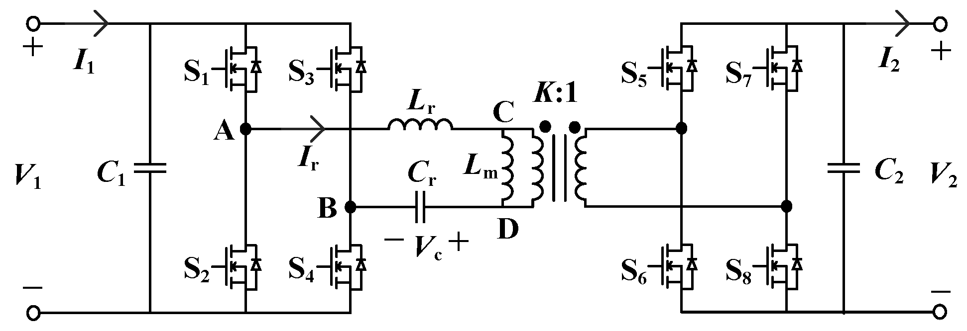
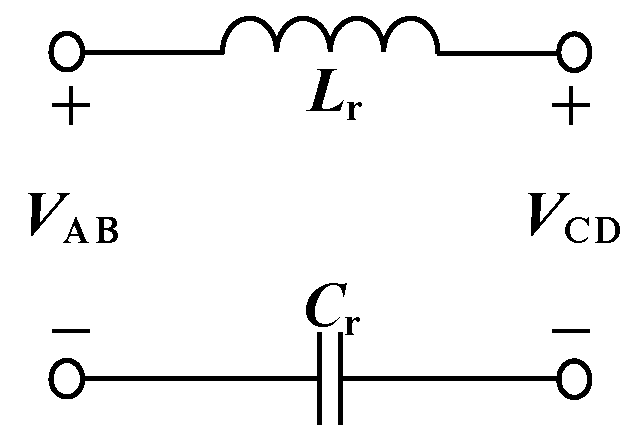
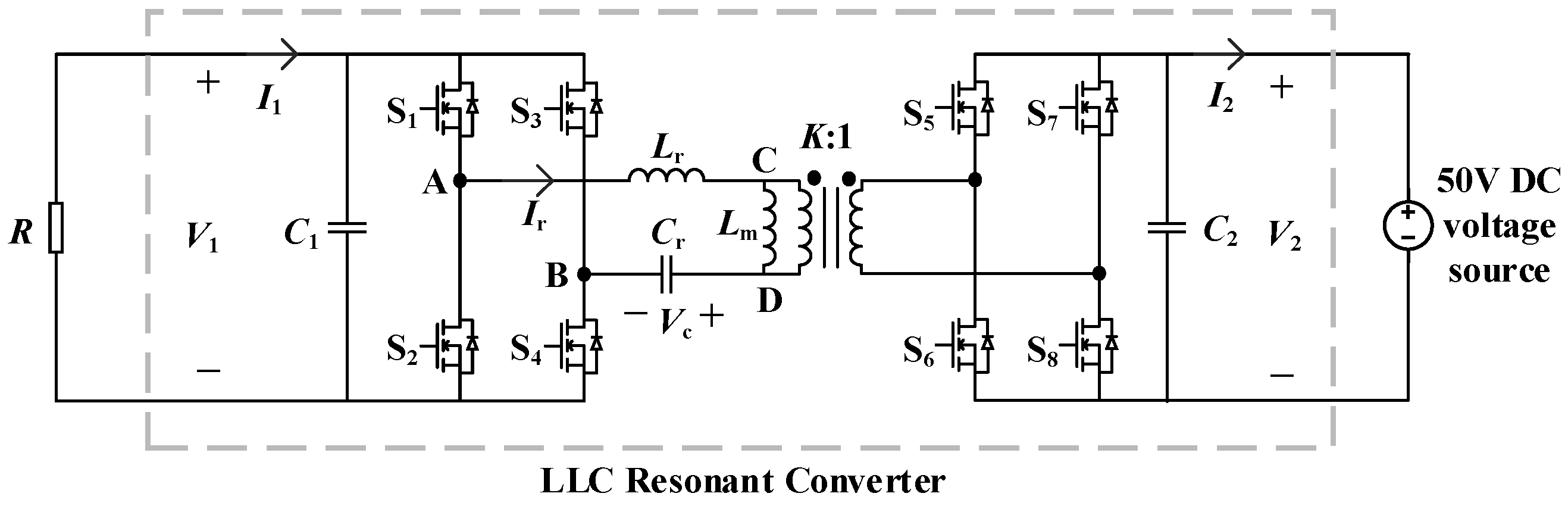
2. Analysis of Operational Characteristics of the Bidirectional LLC Converter

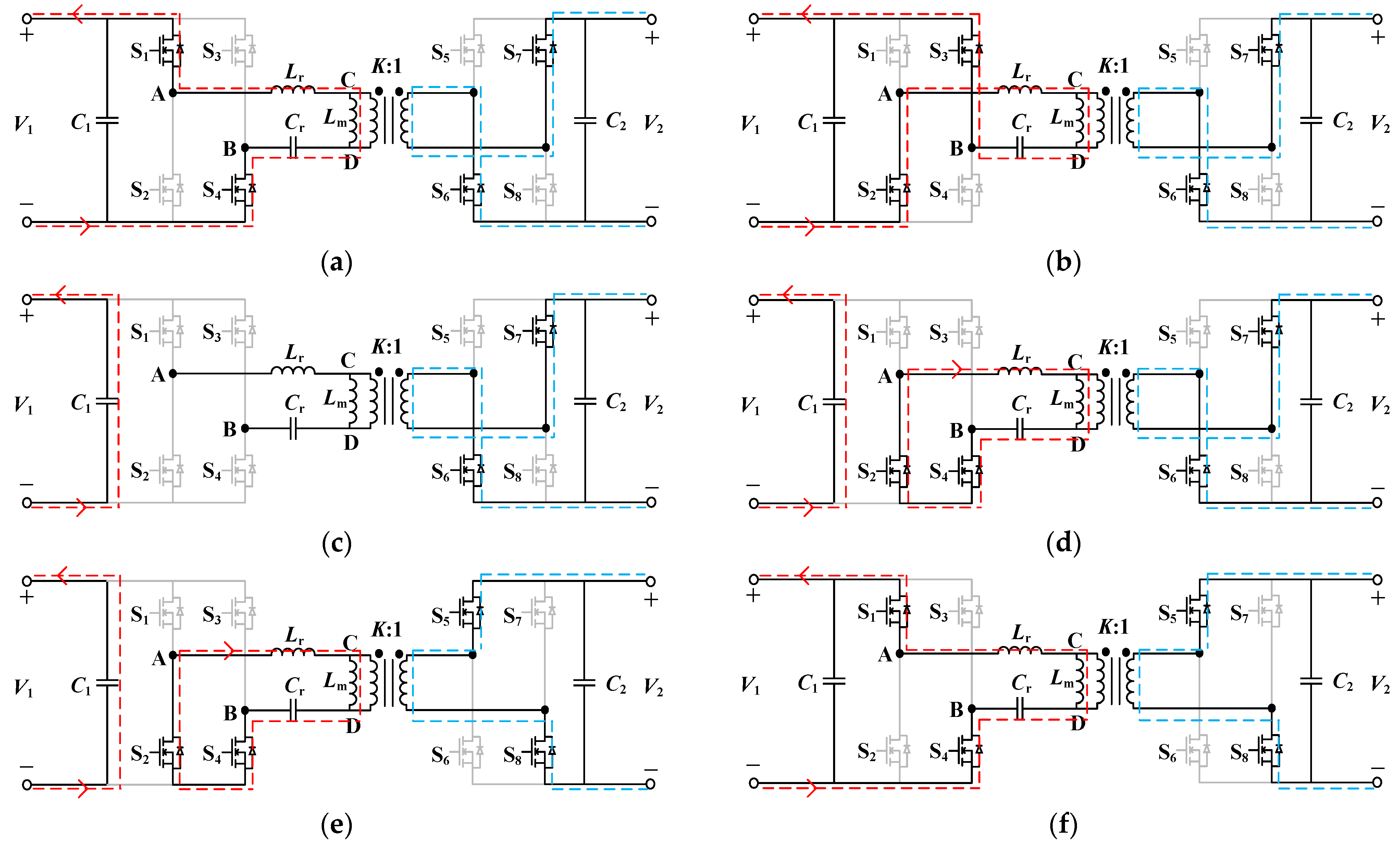
2.1. Bidirectional Mode Analysis

Taking the topology of a full bridge LLC resonant converter (Figure 1) as an example, this paper analyzes various modes of a bidirectional LLC resonant converter.
S1–S4 are primary switches, S5–S8 are secondary side switches, Cr is resonant capacitance, Lr is resonant inductance, Lm is transformer excitation inductance, the transformer turn ratio is K:1, C1 is primary filter capacitance, and C2 is secondary side filter capacitance. V1 is the primary input voltage, V2 is the secondary side output voltage, VC is the voltage on the resonant capacitor, Ir is the current flowing through the resonant inductor, and I1 and I2 are the primary side inflow current and secondary side outflow current, respectively.
According to the power flow direction and normalized gain, LLC resonant converter can be divided into four modes: forward step-up, forward step-down, backward step-up and backward step-down. Among them, there are mature control methods for forward step-up, forward step-down, and backward step-down.
For the backward step-up mode, the driving signal under the fixed resonant frequency is used for the secondary side switches (S5–S8). The primary switches S2 and S4 are used as the active switches, and S1 and S3 are used as the passive switches. The antiparallel freewheeling diodes of the passive switches or synchronous rectification control can be used for rectification. The driving signals of S2 and S6 are consistent. The variable duty cycle control is used for a driving signal of S4, and the duty cycle d changes between 50% and 100%.
When the d of the S4 drive signal is 50% or 100%, the LLC resonant converter is equivalent to working in one of two common working conditions—full bridge or half bridge—and its backward normalized gain is 1 or 2, respectively. By changing the duty cycle d of the S4 drive signal, the converter can switch smoothly between these two working conditions.
For d of 50% and 100%, the waveform characteristics are slightly different. The typical waveforms under the conditions d = 62.5%, 75%, and 87.5% are shown in Figure 2a–c below. The typical waveform under a light load with d = 75% is shown in Figure 2d.
In Figure 2, VAB and VCD represent the voltages between A and B, and C and D, respectively, in Figure 1; Is1Is8 represents the forward current passing through S1–S8; and the equivalent circuit change moments are defined as t0t5.
Figure 2a–c shows that, when the d of S4 gradually increases, the current passing through S3 gradually decreases, the current passing through S4 gradually increases, and the dc bias voltage appears in the resonant capacitor.
This process will lead to uneven heating of S3 and S4, so the backward step-up mode is not suitable for long-term operation, but it has little impact when the load power is small or during short-term operation.
In the backward step-up mode, when the load is heavier, the LLC resonant converter will work in CCM. When the load is lighter, the LLC resonant converter will work in DCM. During t1t2 time period, Ir is constant at 0 in DCM. Typical DCM waveforms are shown in Figure 2d. Under this working condition, Is3 is constant at 0.

2.2. Analysis of Backward Step-Up Mode

Figure 2 shows that, when d and load change, the typical waveforms are slightly different, but they can be divided into six modes. The equivalent circuits of six modes are shown in Figure 3 and analyzed below.
t0t1:
The equivalent circuit in this mode is shown in Figure 3a. At time t0, S4, S5, and S8 are turned off, and the VCD changes from KV2 to −KV2. This time period is the dead time of the secondary side switch’s drive signal, and Is6 and Is7 are negative, the junction capacitance of S6 and S7 can be discharged, and the ZVS on of S6 and S7 can be realized by setting an appropriate dead time. According to the equivalent circuit, the voltage of Lr is (V1 + KV2Vc), and it can be seen in the waveform that when Vc is close to its minimum value, then Ir will increase rapidly and cross zero naturally at t1, making S1 and S4 achieve a ZCS turn off.
t1t2:
This mode can be divided into two equivalent circuits according to the load. It can be equivalent to Figure 3b under CCM and Figure 3c under DCM. At t1, according to the equivalent circuit, when (KV2Vc) ≥ V1, antiparallel freewheeling diodes of S2 and S3 are on, and VAB is −V1. When the load is light and Vc at t1 cannot meet the above conditions, S2 and S3 cannot be turned on. At this time, VAB is (VcKV2). Although the driving signal of S2 will change in this time period, it does not affect the equivalent circuit in this mode.
t2t3:
The equivalent circuit in this mode is shown in Figure 3d. At t2, S4 is hard switched on under CCM and ZVS turn-on in DCM. After S4 is turned on, VAB is forced to change to 0, and the antiparallel freewheeling diode of S3 is turned off. During this time period, energy flows from the secondary side into the resonant tank to charge Lr and Cr.
t3t4:
The equivalent circuit in this mode is shown in Figure 3e. At t3, S6, and S7 are hard switched off, and the VCD changes from −KV2 to KV2. The S2 drive signal becomes 0, but because Is2 is negative and flows through the antiparallel freewheeling diode of S2, similarly to t0t1, S5 and S8 have ZVS turn-on. At t3, the voltage of Lr is (−VcKV2), and it can be seen in the waveform that Vc is close to its maximum value, so Ir will decrease rapidly and cross zero naturally at t4. Although the driving signals of S5 and S8 change during this time period, they do not affect the equivalent circuit in this mode.
t4t5:
The equivalent circuit in this mode is shown in Figure 3f. At t4, S1 realizes ZCS turn-on.
The soft switch characteristics of each switch can be obtained by summarizing the soft switch correlation analysis in the mode analysis, as shown in Table 1. Compared with the forward step-up mode, the backward step-up mode only increases the hard switch loss of S3 and S4 in CCM.

3. Backward Step-Up Voltage Gain

To control the backward output voltage easily, the voltage gain characteristics in the backward step-up mode need to be analyzed. As the typical waveform in the backward step-up mode differs greatly from the sine wave, it is not suitable to use the traditional fundamental harmonic analysis method. We used the time domain analysis method to analyze the control in the backward step-up mode.

3.1. Voltage Gain in CCM

According to the modal analysis in Section 2.2, the equivalent circuit in Figure 3 can be changed into a unified equivalent circuit, as shown in Figure 4.
The time domain equation of each time period can be expressed as:
V cx = I rx 1 Z r sin ( ω r t x ω r t x 1 ) + ( V cx 1 V ABx + V CDx ) cos ( ω r t x ω r t x 1 ) + V ABx V CDx
I rx Z r = I rx 1 Z r cos ( ω r t x ω r t x 1 ) ( V cx 1 V ABx + V CDx ) sin ( ω r t x ω r t x 1 )
where, x can be 1, 2, 3, 4, or 5; Vcx and Irx represent Vc and Ir at tx, respectively; VAbx and VCDx are VAB and VCD in the tx−1tx time period; and Zr and ωr are the resonant impedance and resonant angular frequency, respectively, which can be expressed by the following equation:
{ Z r = L r C r ω r = 1 L r C r
For the t1t2 time period, VAB is −V1 and Ir is not 0 in CCM, and VAB is (VcKV2) and Ir is 0 in DCM, but it does not affect the unified equivalent circuit.
Ignoring the influence of dead time, if the duty cycle of S4 is defined as d, then the following equation exists:
d = t 5 t 2 2 π L r C r
For the convenience of analysis, the time variable is converted into an angle, as shown in the following formula:
{ θ = 2 π ( d 0.5 ) α = ω r ( t 1 t 0 ) β = ω r ( t 4 t 3 )
In CCM, take KV2 as the voltage reference value and (KV2/Zr) as the current reference value, and normalize Equations (1) and (2). Vcxn and Irxn are the unit values of Vcx and Irx, respectively, and G is the backward normalized voltage gain, i.e., G = V1/KV2.
According to the modal analysis in Section 2.2, both Ir1n and Ir4n are 0, Vc0n and Vc5n are equal, and Ir0n and Ir5n are equal. Based on the analysis above, the following approximate assumptions can be made: sin α ≈ 0, cos α ≈ 1, sin ββ, cos β ≈ 1, and (α + θ) ≈ θ. Then, normalized equations can be simplified.
For the unified equivalent circuit of Figure 4, in the steady state, the energy input on the right side in a switching cycle is equal to the energy output on the primary side, so the following energy conservation equation can be obtained:
t 0 t 5 V CD I r d t = V 1 I 1 T r
By simplifying the integral of the resonant inductance current with the value of the resonant capacitance voltage in Equation (6), the following results can be obtained:
V c 0 n V c 3 n = G π I 1 n
where I1n is the per unit value of I1.
By solving simplified normalized equations and the above equations simultaneously, β and G can be obtained:
β = 2 G sin θ 4 ( 1 + cos θ + π I 1 n ) G
G = 8 4 + π I 1 n + 2 cos θ + ( π I 1 n 2 ) 2 8 sin 2 θ
Equation (9) is a more accurate voltage gain, but the calculation is more complex. On the basis of (8), by setting β equal to 0, an approximate expression for the calculation can be obtained, as follows:
G = 4 3 + cos θ

3.2. Voltage Gain in DCM

In DCM, according to the modal analysis, when Ir is constant 0 and Vr does not change between t1 and t2, Ir2n is 0 and Vc2n and Vc1n are equal. Using an analysis method similar to CCM, the following equation can be obtained:
k 3 G 2 + k 4 G + k 5 = 0
where the coefficients k3, k4, and k5 can be expressed by the following equation:
{ k 3 = π I 1 n + cos θ ( 2 cos θ 2 + π I 1 n ) ( cos θ 1 ) 2 k 4 = 4 π I 1 n 6 8 cos θ 1 k 5 = 8 π I 1 n
G in DCM can be solved by using the standard quadratic-root formula, but the gain expression is too complex. At the same time, in DCM conditions, the burst control is often used, so the gain expression in DCM is not detailed in this paper.

3.3. Boundary of CCM and DCM

In Section 2.2, it is known that the boundary of CCM and DCM is dependent on whether the antiparallel freewheeling diode of S3 at time t1 is conductive or not; i.e., the following inequality needs to be satisfied:
K V 2 V c 1 V 1
After normalization, the following inequality is obtained:
V c 1 n + G 1 0
Vc1n can be obtained by combining Equations (7) and (9):
V c 1 n = 1 + 4 ( π I 1 n cos θ 1 ) 4 + π I 1 n + 2 cos θ + ( π I 1 n 2 ) 2 8 sin 2 θ
Therefore, the boundaries of CCM and DCM are as follows:
I 1 n cos θ 1 π

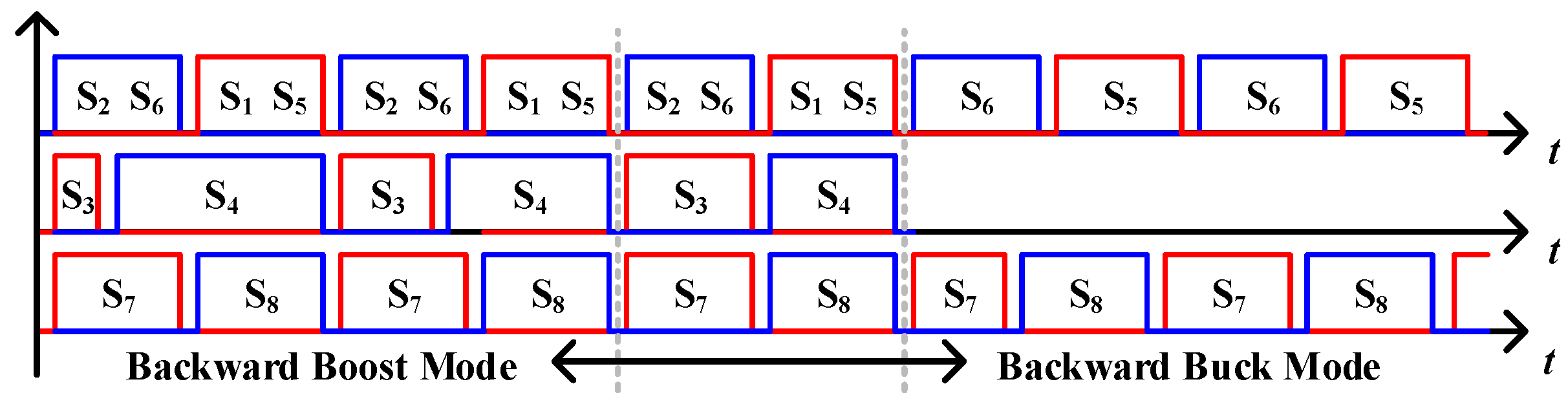
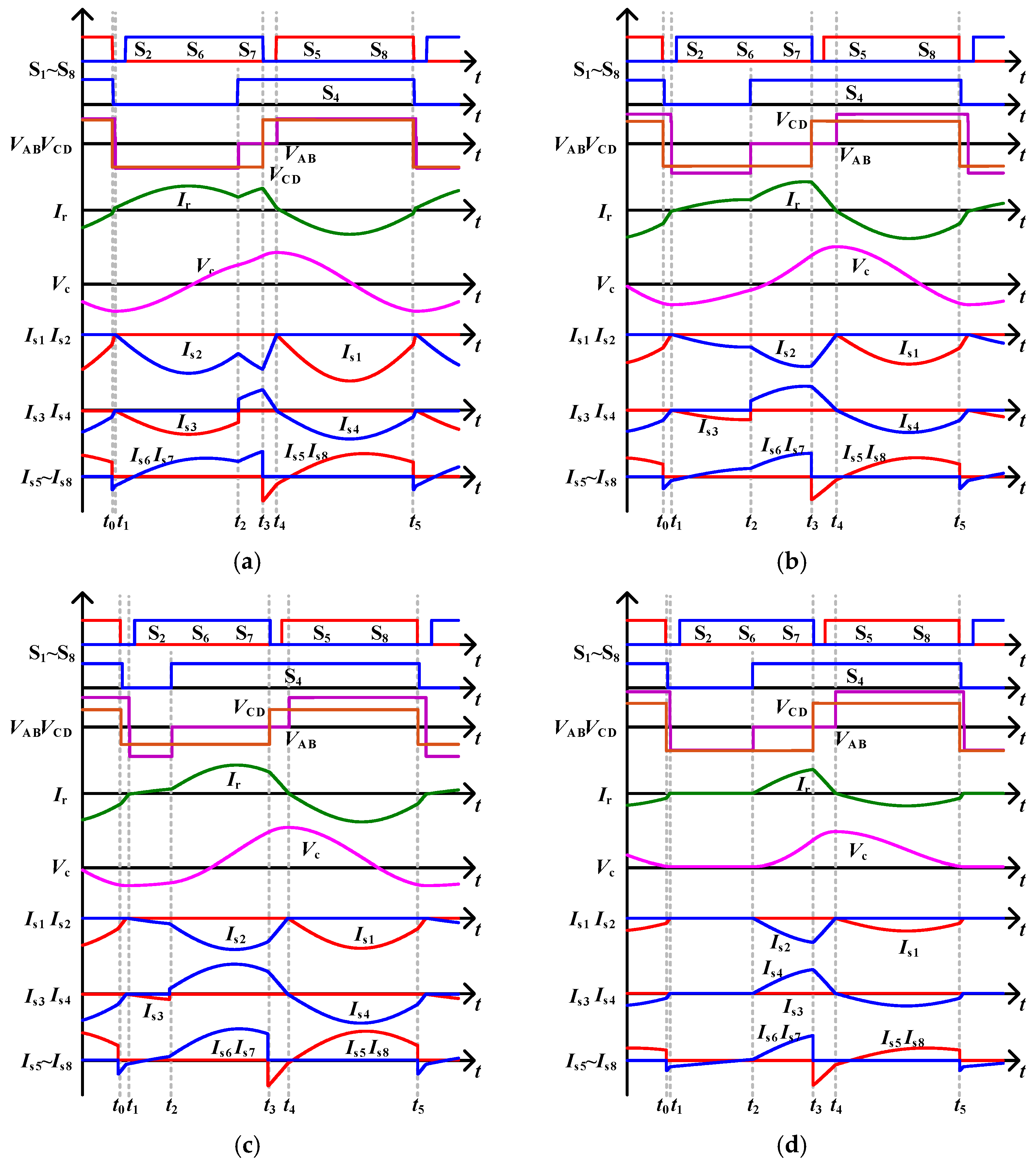
4. Backward Step-Up Control

4.1. Synchronous Rectification Control

S1 and S3 are passive switches, and their current mainly flows through their diodes, which can greatly reduce the on-state loss when synchronous rectification control is used. For bidirectional LLC resonant converters, all switches have driver circuits, so it is easy to achieve synchronous rectification control; that is, S1 and S3 need to be turned on in a specific time period.
According to Figure 2, the turn-on time periods of S1 should be set to t0t1 and t4t5, which have a lot of overlap with the complementary driving signal of S2. The complementary driving signal of S2 can be used for S1, and the dead time tdead between S1 and S2 should be set to (t4t3).
There is a link between (t4t3) and β. Thus, tdead between S1 and S2 can be obtained as follows:
t dead = 4 sin θ L r C r 2 π I 1 n + ( π I 1 n 2 ) 2 8 sin 2 θ
The ideal synchronous rectification effect can be obtained by dynamically adjusting the dead time according to d and I1n. To reduce the control difficulty, tdead can be set to a fixed value, but too much dead time will cause a worse synchronous rectification effect, and too little dead time will cause a hard switch. It can be seen in the characteristics of (17): when I1n is fixed and θ = 0.5π, tdead is the maximum value, and the smaller the fixed value I1n, the larger the maximum value of tdead will be. Therefore, tdead under rated load and θ = 0.5π can be used for the ideal synchronous rectification effect in the full gain range.
For S3, it can use the complementary driving signal of S4 in CCM, but cannot be turned on in DCM, so (16) can be used as a criterion to determine the driving signal of S3.

4.2. Smooth Transition between Backward Step-Up Mode and Backward Step-Down Mode

The backward step-up mode with synchronous rectification control can make the LLC converter enter the fixed frequency operation mode by adjusting the duty cycle d to 50%. Then, the driving signals of the secondary side switches can be shifted to make the LLC converter switch smoothly into backward step-down mode using phase-shift control. The switching process is shown in Figure 5.
Synchronous rectification control is not used for the backward step-down mode in Figure 5, so S1–S4 have no driving signal after entering the backward step-down mode. A synchronous rectifier controller can be used in the backward step-down mode to reduce the loss of the antiparallel diodes, but it is not the focus of this paper, so it is not described in detail.
Similarly, in the backward step-down mode, the phase shift angle is gradually adjusted to 0, the LLC converter enters the fixed frequency mode, and the duty cycle of S4 is gradually increased to make the LLC converter switch smoothly into the backward step-up mode.

5. Comparison with Previous Studies

In order to highlight the advantages of the method proposed in this paper, it is compared with the previous studies in many aspects. The proposed method, the method with changing topology, and the method in [23] are compared and analyzed in Table 2. The method with changing topology takes a CLLLC converter as an example.
Through the simulations under the same operating conditions with the same resonance parameters, the following conclusions were obtained.
The proposed method does not need to change the LLC topology, so it does not affect the efficiency of the converter in forward mode. The steady-state characteristics of the proposed control strategy are slightly worse than those of the CLLLC resonant converter, but its structure is simple and it is easy to implement at low cost. At the same time, it has obvious advantages in the loss compared with the method in [23].
This method cannot improve the efficiency and ripple characteristics, and is not suitable for steady-state operation, but it is more suitable for temporary conditions or low-power conditions in backward step-up mode, such as temporary outward power scenarios for electric vehicle batteries.

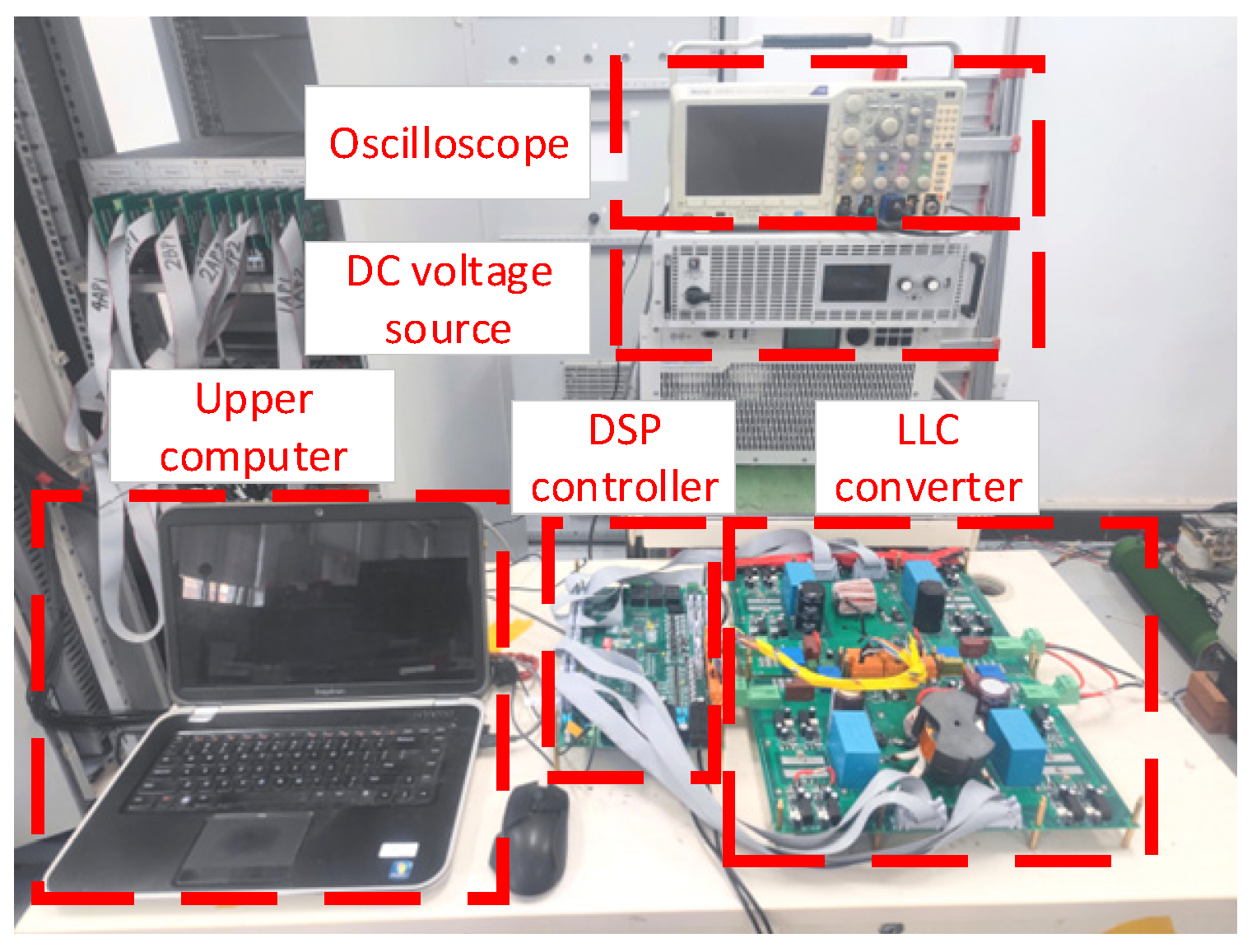
6. Experimental Verification

To verify the validity of the control strategy proposed in this paper, a full-bridge LLC resonant converter was built with C3M0025065D silicon carbide (SiC) MOSFETs. One side of it was connected with a 50-volt (V) DC voltage source, and the other side was connected to a load R (Figure 6).
The actual experimental platform is shown in the Figure 7. The experimental platform used DSP as the controller, the upper computer for communication, and a Tektronix oscilloscope to observe the waveform.
Table 3 shows the related parameters of the LLC resonant converter. The dead time of S1 and S2 was 547 nanoseconds (ns), which was estimated from (17), and was set to 550 ns in the experiment.

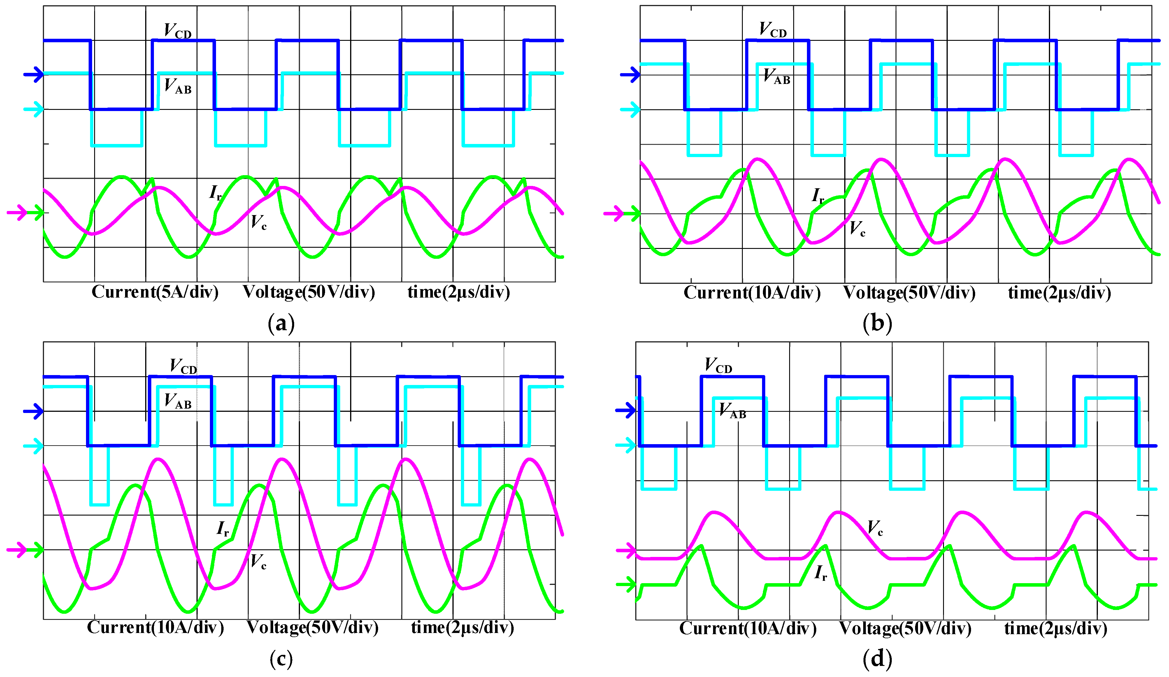
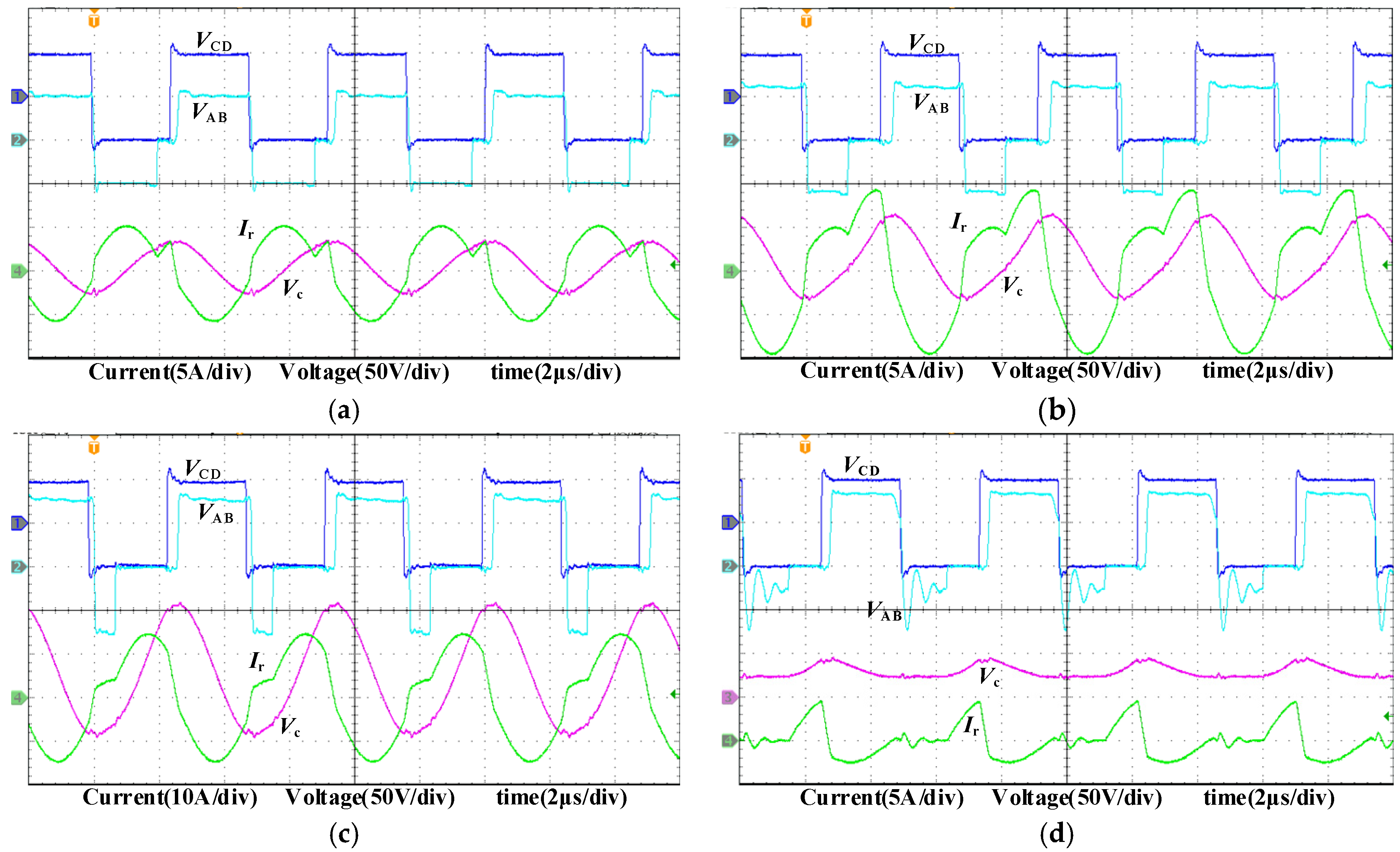
6.1. Backward Step-Up Mode Analysis Verification

Simulations and experiments were conducted at different duty cycles to verify the validity of the backward step-up mode analysis in Section 2.1. They were conducted with V2 = 50 V, R = 15 Ω at d = 62.5%, 75%, and 87.5%; and V2 = 50 V and R = 35 Ω in DCM at d = 75%. The waveforms of Vc, Ir, VAB, and VCD are shown in Figure 8 and Figure 9.
It can be seen in Figure 8 and Figure 9 that the experimental waveforms with different duty cycles are basically the same as the simulation waveforms. There are some differences in amplitude between the experimental waveforms and the simulation waveforms that were affected by some unsatisfactory factors in the experiment, but they are basically consistent with the theoretical modal analysis. The feasibility of the backward step-up mode and the validity of the modal analysis were verified.
For the DCM waveforms in Figure 9d, Ir appears close to discontinuity. Due to the existence of distribution parameters in the circuit, Ir oscillates to a certain extent near 0 and causes a large fluctuation of VAB, but it has little influence on the mode analysis.

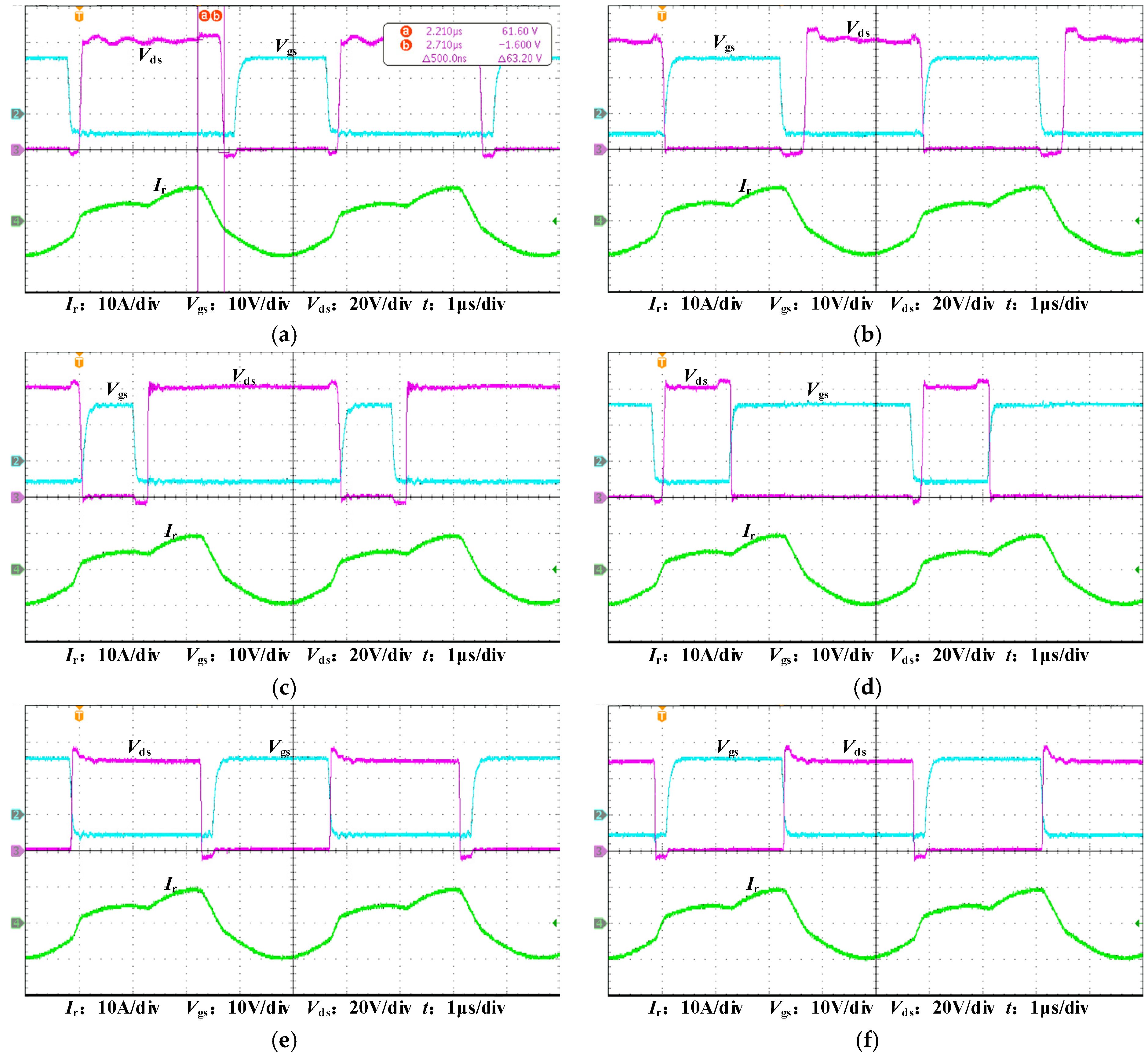
6.2. Verification of Soft Switch Characteristics and Synchronous Rectification Control

To verify the soft switch characteristics, the Vds and Vgs of the switches were observed under the condition of rated load and 75% duty cycle, and Ir was used as the reference line, as shown in Figure 10.
Figure 10a,b shows that S1 and S2 both produced a diode conduction voltage drop after ZCS by Ir zero-crossing; then, synchronous rectification was achieved under the influence of the driving signal, without affecting the soft switch effect.
Similarly, S3 achieved ZCS turn-on and S4 achieved ZCS turn-off, but the drive signal of S4 made S4 hard switch on, and S3 was forcibly hard switched off.
The waveforms of S5 and S6 are the same as those of S8 and S7, respectively. It can be seen in Figure 10e,f that S5–S8 achieved ZVS turn-on, but no ZVS turn-off. The soft switch effects of the switches were in concordance with the theoretical analysis, which further verifies the correctness of the theoretical analysis.
At the same time, it can be seen in Figure 10a that the time at which Ir began to decrease after S1 was turned on was about 500 ns, which is close to the estimated 547 ns. The synchronous rectification effect of S1 is ideal. In Figure 10c, it can be seen that S3 achieved an ideal synchronous rectification effect by using a driver signal complementary to S4. Therefore, the validity of synchronous rectification control was verified.

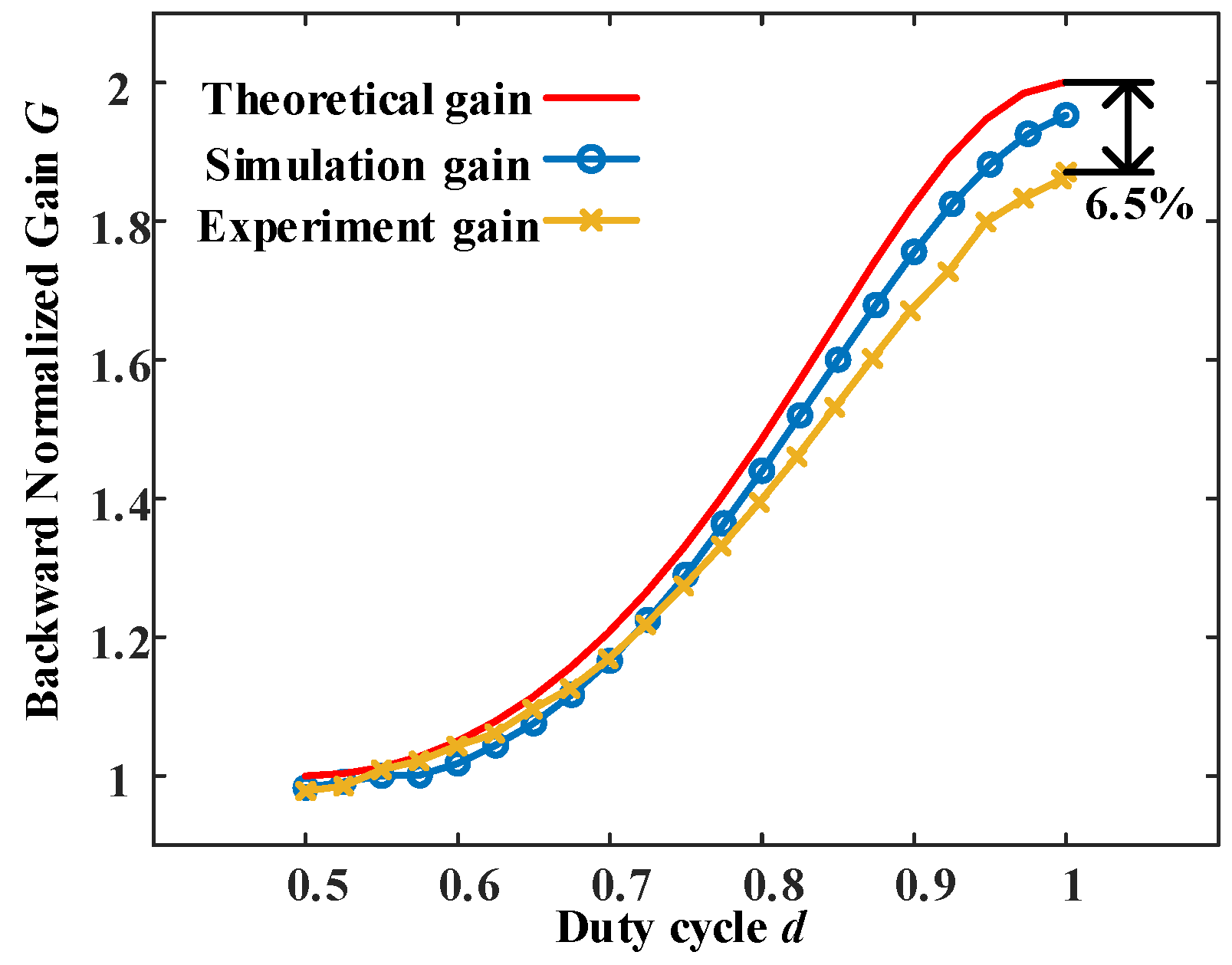
6.3. Verification of Voltage Gain

We measured the voltage gain curves of simulation and experiment under rated load and compared them with the theoretical gain curve. The results are shown in Figure 11.
From Figure 11, it can be seen that the trends of theoretical, simulation, and experimental gain curves with d are approximately the same, which verifies the rationality of the backward step-up normalized gain expression.
The theoretical gain in Figure 11 was approximately the same as the simulated gain, but there was still a small error due to the use of some approximate assumptions in the derivation of the theoretical gain. As the duty cycle increased, the error between experimental gain and theoretical gain increased, with a maximum relative error of 6.5% relative to theoretical gain. Except for errors caused by approximate assumptions, the main cause of error was that with the increase in the backward gain, the output power increased by a square factor while the load resistance remained unchanged, and the loss on the switches and the magnetic element also increased, so the error increased.
As shown in the voltage gain curve in Figure 11, the backward normalized step-up gain near 2 can be achieved by adjusting the duty cycle.

7. Conclusions

This paper presented a bidirectional control strategy that functions without changing the topology of the LLC resonant converter. In backward step-up mode, the variable duty cycle control with the drive signal of the primary side switches was proposed and used. The traditional control was used for forward step-down mode, forward step-up mode, and backward step-down mode. The backward step-up normalized gain can vary from one to two at the resonant frequency, and the smooth transition between the backward step-up mode and the backward step-down mode can be achieved. At the same time, the expression of voltage gain under backward step-up control was deduced, the boundaries of CCM and DCM were given, and the corresponding synchronous rectification method was given, which can enable the soft switching of most switches.

Author Contributions

Conceptualization, J.N.; methodology, J.N. and Y.T.; validation, J.N. and Y.W.; formal analysis, J.N. and L.J.; investigation, J.N. and X.W.; writing—review and editing, J.N. and X.W.; supervision, X.W. and W.Z. All authors have read and agreed to the published version of the manuscript.

Funding

This research was funded by Delta Power Electronics Science and Education Development Plan, grant number DREK2021005.

Institutional Review Board Statement

Not applicable.

Informed Consent Statement

Not applicable.

Data Availability Statement

The data presented in this study are available on request from the corresponding author. The data are not publicly available as the data also forms part of an ongoing study.

Conflicts of Interest

The authors declare no conflict of interest.

References

  1. Musavi, F.; Craciun, M.; Gautam, D.S.; Eberle, W.; Dunford, W.G. An LLC Resonant DC–DC Converter for Wide Output Voltage Range Battery Charging Applications. IEEE Trans. Power Electron. 2013, 28, 5437–5445. [Google Scholar] [CrossRef]
  2. Wang, C.-S.; Zhang, S.-H.; Wang, Y.-f.; Chen, B.; Liu, J.-H. A 5-kW Isolated High Voltage Conversion Ratio Bidirectional CLTC Resonant DC–DC Converter With Wide Gain Range and High Efficiency. IEEE Trans. Power Electron. 2019, 34, 340–355. [Google Scholar] [CrossRef]
  3. Ortiz, G.; Leibl, M.G.; Huber, J.E.; Kolar, J.W. Design and Experimental Testing of a Resonant DC–DC Converter for Solid-State Transformers. IEEE Trans. Power Electron. 2017, 32, 7534–7542. [Google Scholar] [CrossRef]
  4. Zhou, A.A.; Yang, B.X.; Tian, C.M.; Wang, D.N.; Wang, E.L. Analysis and Design of LLC Resonant Converters Operating in Reverse Mode. In Proceedings of the 2019 10th International Conference on Power Electronics and ECCE Asia (ICPE 2019—ECCE Asia), Busan, Korea, 27–30 May 2019. [Google Scholar] [CrossRef]
  5. Zhang, J.; Liu, J.; Yang, J.; Zhao, N.; Wang, Y.; Zheng, T.Q. An LLC-LC Type Bidirectional Control Strategy for an LLC Resonant Converter in Power Electronic Traction Transformer. IEEE Trans. Power Electron. 2018, 65, 8595–8604. [Google Scholar] [CrossRef]
  6. Wang, S.; Zhang, Z.; Zhang, J.; Zhu, W.; Ren, X.; Hu, C. A Bidirectional Synchronous/Asynchronous Rectifier Control for Wide Battery Voltage Range in SiC Bidirectional LLC Chargers. IEEE Trans. Power Electron. 2022, 37, 6090–6101. [Google Scholar] [CrossRef]
  7. Li, Y.; Shao, S.; Chen, S.; Zhang, J.; Sheng, K. High-gain high-efficiency IPOS LLC converter with coupled transformer and current sharing capability. CPSS Trans. Power Electron. Appl. 2020, 5, 63–73. [Google Scholar] [CrossRef]
  8. Ma, J.; Wei, X.; Hu, L.; Zhang, J. LED Driver Based on Boost Circuit and LLC Converter. IEEE Access 2018, 6, 49588–49600. [Google Scholar] [CrossRef]
  9. Lee, J.; Jeong, Y.; Han, B. A Two-Stage Isolated/Bidirectional DC/DC Converter With Current Ripple Reduction Technique. IEEE Trans. Power Electron. 2012, 59, 644–646. [Google Scholar] [CrossRef]
  10. Liao, Y.; Peng, T.; Su, M.; Sun, Y.; Xiong, W.; Xu, G. A Bidirectional DAB-LLC DCX to Achieve Voltage Regulation and Wide ZVS Range Capability. In Proceedings of the 2020 22nd European Conference on Power Electronics and Applications (EPE’20 ECCE Europe), Lyon, France, 7–11 September 2020; pp. 1–8. [Google Scholar] [CrossRef]
  11. Liao, Y.; Xu, G.; Sun, Y.; Peng, T.; Su, M.; Guo, B.; Xiong, W. Single-Stage DAB-LLC Hybrid Bidirectional Converter With Tight Voltage Regulation Under DCX Operation. IEEE Trans. Ind. Electron. 2021, 68, 293–303. [Google Scholar] [CrossRef]
  12. Li, X.; Huang, J.; Ma, Y.; Wang, X.; Yang, J.; Wu, X. Unified Modeling, Analysis, and Design of Isolated Bidirectional CLLC Resonant DC–DC Converters. IEEE J. Emerg. Sel. Top. Power Electron. 2022, 10, 2305–2318. [Google Scholar] [CrossRef]
  13. Zuo, Y.; Pan, X.; Zhu, J.; Ye, J.; Wang, Y. A Bidirectional Isolated LLC Resonant Converter with Configurable Structure for Wide Output Voltage Range Applications. In Proceedings of the 2020 IEEE 9th International Power Electronics and Motion Control Conference (IPEMC2020-ECCE Asia), Nanjing, China, 29 November–2 December 2020; pp. 1716–1721. [Google Scholar] [CrossRef]
  14. He, P.; Mallik, A.; Sankar, A.; Khaligh, A. Design of a 1-MHz High-Efficiency High-Power-Density Bidirectional GaN-Based CLLC Converter for Electric Vehicles. IEEE Trans. Veh. Technol. 2019, 68, 213–223. [Google Scholar] [CrossRef]
  15. Lin, F.; Zhang, X.; Li, X. Design Methodology for Symmetric CLLC Resonant DC Transformer Considering Voltage Conversion Ratio, System Stability, and Efficiency. IEEE Trans. Power Electron. 2021, 36, 10157–10170. [Google Scholar] [CrossRef]
  16. Min, J.; Ordonez, M. Bidirectional Resonant CLLC Charger for Wide Battery Voltage Range: Asymmetric Parameters Methodology. IEEE Trans. Power Electron. 2021, 36, 6662–6673. [Google Scholar] [CrossRef]
  17. Zhang, F.; Wang, Y.; Wang, F.; Ming, J. Synchronous Rectification Control Strategy for Bidirectional Full-bridge LLC Resonant Converter. In Proceedings of the 22nd International Conference on Electrical Machines and Systems (ICEMS), Harbin, China, 11–14 August 2019; pp. 1–6. [Google Scholar] [CrossRef]
  18. Jiang, T.; Zhang, J.; Wu, X.; Sheng, K.; Wang, Y. A Bidirectional LLC Resonant Converter With Automatic Forward and Backward Mode Transition. IEEE Trans. Power Electron. 2015, 30, 757–770. [Google Scholar] [CrossRef]
  19. Jaiswal, V.K.; Ghoshal, A. A Design Methodology of Bidirectional LLC Resonant Converter for Energy Storage Systems. In Proceedings of the 2019 IEEE Transportation Electrification Conference and Expo, Asia-Pacific (ITEC Asia-Pacific), Seogwipo, Korea, 8–10 May 2019; pp. 1–6. [Google Scholar] [CrossRef]
  20. Kim, E.-S.; Park, J.-H.; Joo, J.-S.; Lee, S.-M.; Kim, K.; Kong, Y.-S. Bidirectional DC-DC Converter using Secondary LLC Resonant Tank. In Proceedings of the 2015 IEEE Applied Power Electronics Conference and Exposition (APEC), Charlotte, NC, USA, 15–19 March 2015; pp. 2104–2108. [Google Scholar] [CrossRef]
  21. Jiang, T.; Zhang, J.; Wu, X.; Sheng, K.; Wang, Y. A Bidirectional Three-Level LLC Resonant Converter With PWAM Control. IEEE Trans. Power Electron. 2016, 31, 2213–2225. [Google Scholar] [CrossRef]
  22. Deng, G.; Ouyang, Q.; Xu, G.; Sun, Y.; Su, M. Modified Topology and PWM Modulation for Bidirectional LLC-DCX Converter with Center-Tapped Transformer. In Proceedings of the 2021 IEEE 4th International Electrical and Energy Conference (CIEEC), Wuhan, China, 28–30 May 2021; pp. 1–5. [Google Scholar] [CrossRef]
  23. He, J.; Zhang, J.; Ma, H. Design of a Bi-directional Full Bridge LLC Resonant Converter with a Higher Normalized Voltage Gain under Backward Mode. In Proceedings of the 2017 19th European Conference on Power Electronics and Applications (EPE’17 ECCE Europe), Warsaw, Poland, 11–14 September 2017; pp. 1–9. [Google Scholar] [CrossRef]
Figure 1. Topology of an LLC resonant converter.
Energies 15 04471 g001
Figure 2. Typical waveforms of the step-up control strategy under the backward mode. (a) d = 62.5%, (b) d = 75%, (c) d = 87.5%, (d) light load.
Energies 15 04471 g002
Figure 3. Equivalent circuit under different modes. (a) t0t1, (b) t1t2 (CCM), (c) t1t2 (DCM), (d) t2t3, (e) t3t4, (f) t4t5.
Energies 15 04471 g003
Figure 4. Unified equivalent circuit.
Energies 15 04471 g004
Figure 5. The drive signal during mode switching.
Energies 15 04471 g005
Figure 6. Structural diagram of the experimental platform.
Energies 15 04471 g006
Figure 7. Actual experimental platform.
Energies 15 04471 g007
Figure 8. Simulation waveforms with different conditions. (a) d = 62.5%, (b) d = 75%, (c) d = 87.5%, (d) DCM.
Energies 15 04471 g008
Figure 9. Experimental waveforms with different conditions. (a) d = 62.5%, (b) d = 75%, (c) d = 87.5%, (d) DCM.
Energies 15 04471 g009
Figure 10. Soft switching waveforms of S1–S6. (a) S1, (b) S2, (c) S3, (d) S4, (e) S5, (f) S6.
Energies 15 04471 g010
Figure 11. Voltage gain comparison.
Energies 15 04471 g011
Table 1. The soft switching characteristics of switches.
Switch NameTurn-OnTurn-Off
S1ZCSZCS
S2ZCSZCS
S3ZCSHard switch in CCM
ZCS in DCM
S4Hard switch in CCM
ZCS in DCM
ZCS
S5 and S8ZVSHard switch
S6 and S7ZVSHard switch
Table 2. The comparison between the proposed method and other methods.
The Proposed MethodThe Method with
Changing Topology
The Method in [23]
Additional componentsNoYesNo
Efficiency in forward modeNo influenceSome influenceNo influence
Efficiency in backward modeSlightly lowerHighLow
Parameter design difficultyLowHighLow
Control difficultyLowHighHigh
Smooth Transition between different modesYesYesNo
Ripple characteristicsSlightly highLowSlightly high
Table 3. The design parameters of the prototype.
Parameter NameValue
Resonance frequency fr/kHz207
Transformer turn ratio1
Resonance inductance Lr/μH4
Resonance capacitor Cr/nF142
Excitation inductance Lm/μH19.45
Secondary side voltage V2/V50
Primary side rated load R15
Publisher’s Note: MDPI stays neutral with regard to jurisdictional claims in published maps and institutional affiliations.

