1. Introduction
Worldwide, as global warming and environmental pollution become more severe, super grid projects that share electric power by linking electric power systems between countries and continents are drawing attention. Super grids can contribute greatly to the reduction of greenhouse gases and fine dust through efficient energy distribution, stabilization of energy supply and demand, and utilization of new and renewable energy sources. Therefore, in the European Union (EU), the Nord EU Super grid and Sud EU-Middle East and North Africa (MENA) Super grid projects are being promoted to reduce greenhouse gases and establish a single electricity market [
1,
2,
3,
4]. In addition, in Northeast Asia, the Northeast Asia Power System Interconnection (NAPSI) project is being planned to establish a strategy for linking power systems between Korea, Japan, China, Russia, and Mongolia [
5,
6,
7].
High-voltage direct current (HVDC) technology is advantageous for long-distance transmission due to its high transmission efficiency. Additionally, the small size of the transmission tower is advantageous both environmentally and economically. Furthermore, when the grid is connected, the increase in short-circuit capacity can be suppressed and the connection of two systems with different frequencies is possible [
8,
9,
10,
11,
12,
13,
14]. Therefore, HVDC technology is essential to stably operate a super grid.
HVDC cable is the core technology of the HVDC system for high-capacity and long-distance power transmission, and includes mass impregnated (MI) cable, MI-polypropylene laminated paper (MI-PPLP) cable, oil-filled (OF) cable, cross-linked polyethylene (XLPE) cable, etc. [
14]. HVDC MI cables are non-draining cables using kraft paper impregnated with mass in an insulating layer and have been used for the past 60 years. However, since the maximum operating temperature of the cable is 50–55 °C, high-capacity transmission has not been possible [
15,
16]. Therefore, based on the excellent dielectric and temperature characteristics of PPLP paper, MI-PPLP cables (maximum operating temperature of 85 °C) were developed and applied to various commercial projects such as the Western Link and Bukdangjin-Goduk (South Korea) [
17,
18,
19,
20]. However, since HVDC MI-PPLP cable has not been officially operated due to various problems, verification of the reliability of the cable is required.
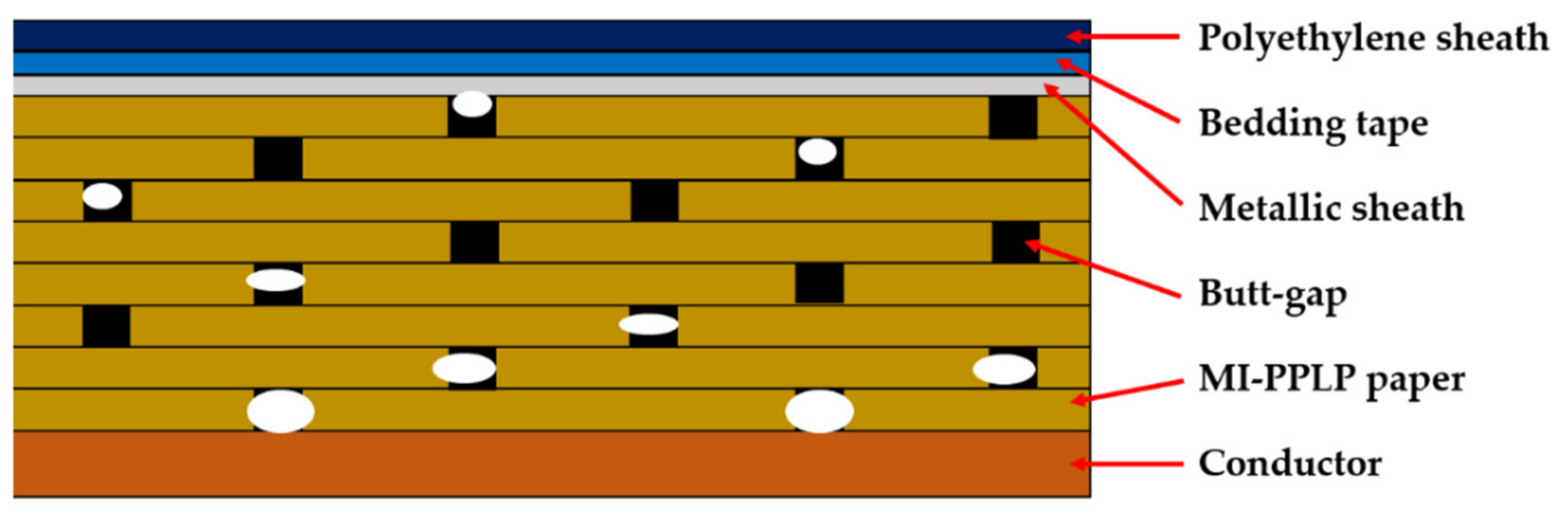
Void defects formed in the butt-gap of HVDC MI-PPLP cables greatly affect the insulation reliability of the cables. Commonly, a butt-gap is formed during the process of winding the insulating paper, and allows oil to flow freely between layers of insulating paper during the oil impregnation process. However, during the cooling period after load reduction or turn-off of the MI-PPLP cable, voids may form in the butt-gap on the conductor side by cavitation, as shown in
Figure 1 [
15,
21,
22]. The electrical conductivity of the void is about 100 times higher than the electrical conductivity of MI-PPLP. Therefore, when the electric field is concentrated at the interface between the void and MI-PPLP due to the difference in electrical conductivity between void and MI-PPLP, partial discharge occurs, and eventually electrical and thermal aging may occur [
15,
16,
23]. That is, dielectric breakdown may occur as the dielectric strength of the cable decreases [
24,
25,
26]. Therefore, to diagnose defects in the insulation of HVDC MI-PPLP cables, it is necessary to study the direct current (DC) void discharge and the pre-symptoms of dielectric breakdown.
Typically, a partial discharge measurement is used to verify the reliability of cables. The partial discharge measurement method is the same for either alternating current (AC) voltage or DC voltage [
27]. However, pattern analysis of partial discharge depends on the type of applied voltage. In the case of AC partial discharge, partial discharge occurs according to the phase of the voltage pulsating in one period of the applied voltage. Therefore, it can be analyzed using a phase-resolved partial discharge (PRPD) and a phase-resolved pulse sequence (PRPS), which are analyzed using the phase, magnitude, and frequency of the partial discharge pulse. AC partial discharge characteristics of each defect have been studied sufficiently, and are currently used for insulation diagnosis of High-voltage alternating current (HVAC) cables [
28,
29,
30,
31,
32]. In the case of DC partial discharge, since there is no phase information as there is with AC voltage, the same analysis method used for AC partial discharge cannot be used. Therefore, to analyze the DC partial discharge, the pulse sequence analysis (PSA) method based on the magnitude of the discharge and the time difference between the discharge pulses is used [
33,
34,
35,
36,
37]. However, sufficient studies on experimental standards, pattern analysis, diagnostic methods, and discharge characteristics have not been conducted. Therefore, studies on DC partial discharge measurements and characteristic analysis are required.
In this paper, the patterns of DC void discharge according to the temperature and applied voltage of the specimen were analyzed to develop an insulation diagnosis method for void defects in HVDC MI-PPLP cables. When the applied voltage is smaller than the partial discharge inception voltage (
PDIV), partial discharge does not occur, and when the applied voltage is larger than the breakdown voltage (
BDV), insulation breakdown occurs. Therefore, the magnitude of the voltage applied to measure DC void discharge was selected between the lowest value of
BDV and the highest value of
PDIV based on our previous paper [
38]. In a recently published paper [
34,
36,
37], patterns of DC partial discharge were analyzed using PSA for various defects. However, the time-frequency (TF) mapping technique was not applied, which is a method to remove external noise and distinguish discharges from various defects. However, in this research, in order to minimize the influence of external noise, which is a disadvantage of the PSA method, various noises other than void discharge were removed using TF mapping, and then the DC void discharge patterns were analyzed. In addition, to confirm the pre-symptoms of insulation breakdown caused by void discharge, void discharge was maintained until insulation breakdown occurred. Then, based on the patterns of DC void discharge, the pre-symptoms of dielectric breakdown due to void defects in the MI-PPLP cable were confirmed.
2. DC Void Discharge Measurement Process
2.1. Void Defect and Test Jig Structure
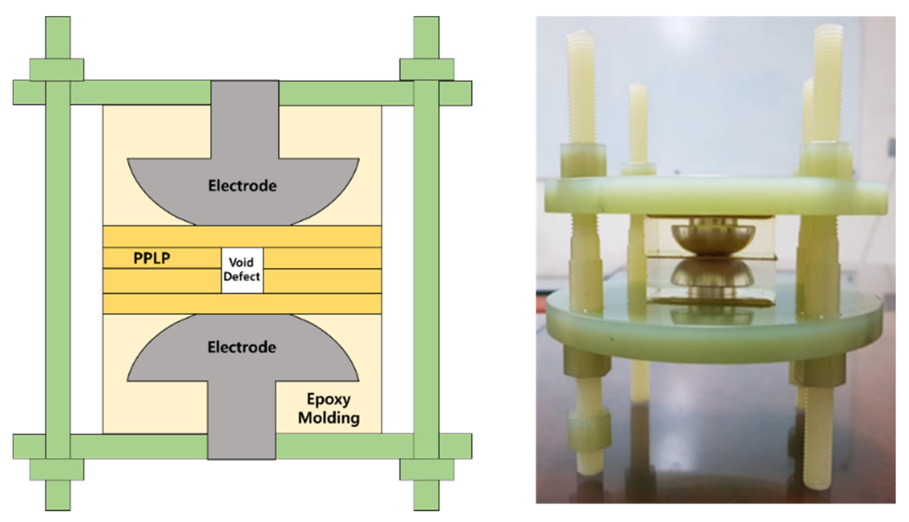
The test cell used to simulate void discharge in the MI-PPLP cable is shown in
Figure 2. The electrodes were made of stainless steel, and the diameter of the effective area was 12 mm and the radius of curvature was 11 mm. In addition, the electrode was molded with epoxy to block electrical noise (creepage breakdown, surface discharge, and edge effects) excluding void discharge signals. The test jig was fabricated of glass fiber reinforced plastic (GFRP), which has excellent mechanical and dielectric strength, and was designed so that partial discharge did not occur in the test jig due to the high electric field.
To simulate MI-PPLP, PPLP with an area of 50 mm × 50 mm and a thickness of 0.125 mm was impregnated into the mass using the following process. First, the moisture and air of the PPLP were removed by maintaining a vacuum below 0.8 torr using a vacuum pump. Next, the PPLP was impregnated for 96 h in a degassed mass of 100 degrees so that the polypropylene (PP) and kraft were completely impregnated without heat damage. Then, specimens with four laminated layers of PPLP were fabricated so that the circular butt-gap with a diameter of 2 mm was overlapped in the 2nd and 3rd layers. This was intended to simulate an instance where the two layers of butt-gaps overlap in the layer where the cable is bent or the wrapping direction of the PPLP is changed. Finally, a pressure of 3 bar, similar to the tension of the MI-PPLP cable, was applied equally to each specimen using a load cell.
2.2. DC Partial Discharge Measurement System
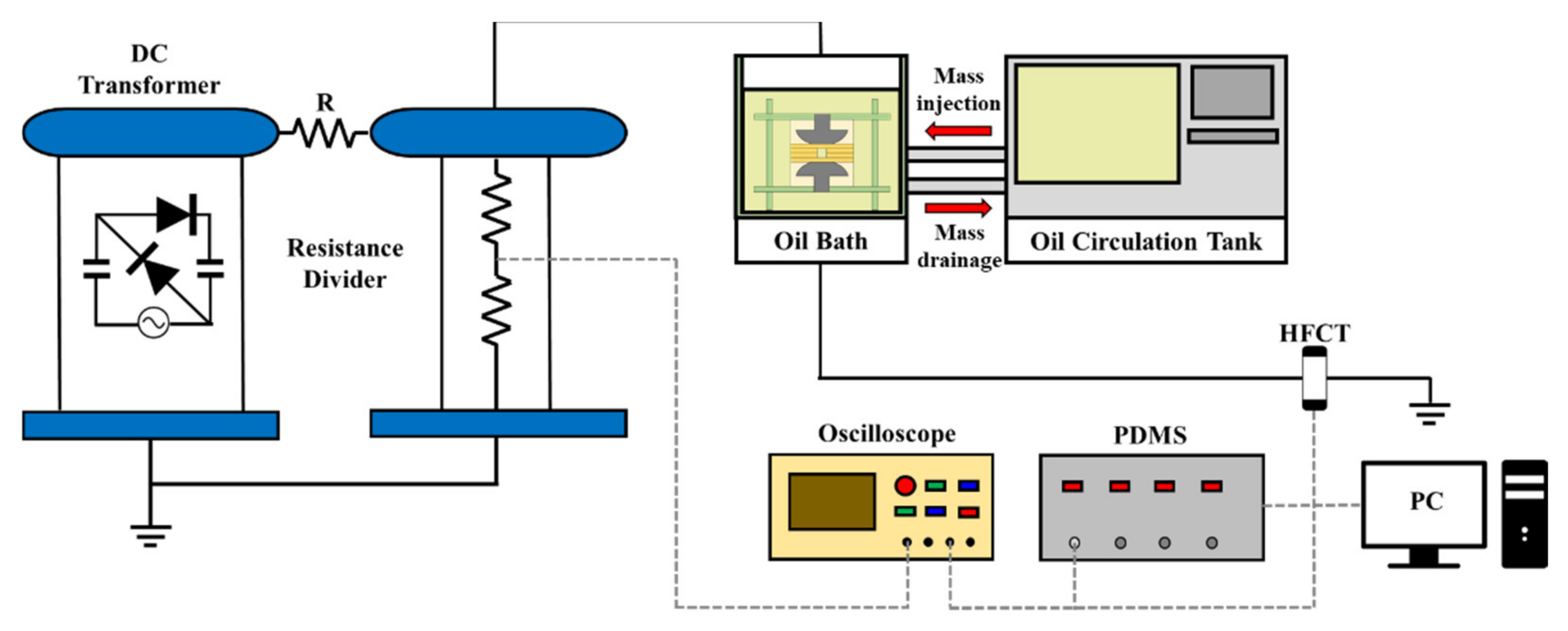
The block diagram of the experimental circuit for DC void discharge measurements is shown in
Figure 3. DC partial discharge measurements for void defects were conducted using a DC transformer, oil bath, oil circulation tank, oscilloscope, partial discharge measurement system (PDMS), high frequency current transformer (HFCT) sensor, and personal computer (PC); descriptions of each piece of equipment are as follows.
The noise generated by DC ripple voltage affects the partial discharge measurement experiment [
27]. Therefore, to minimize the noise, a DC transformer with less than 1% ripple was used. In a DC electric field, the temperature of the specimen affects the conductivity, and the conductivity affects the DC partial discharge characteristics [
39,
40]. The oil bath and oil circulation tank are filled with high viscosity mass to simulate the environment of the MI-PPLP cable. The oil circulation tank sets and maintains the temperature of the oil, and has the function of injecting and draining oil between the oil circulation tank and the oil bath. Therefore, to analyze the partial discharge characteristics according to the temperature of the specimen, an oil circulation tank was connected to continuously inject the mass heated to the experimental temperature into the oil bath. Further, the void discharge pulse was acquired using an HFCT sensor that measures the leakage current due to discharge, and the presence or absence of discharge and the shape of the void discharge pulse were confirmed using an oscilloscope. Finally, after void discharge was confirmed through the oscilloscope, a PDMS connected to a PC was used to analyze the characteristic partial discharge pulse. A PDMS is a device that can record the occurrence time and magnitude of the partial discharge pulse in real time, and can analyze pulse and frequency of partial discharge. The detection frequency range was up to 50 MHz, and the sampling rate of the discharge pulse was greater than 100 MS/s.
To analyze the DC void discharge characteristics according to temperature, the temperatures of the specimen were set at 55 °C, 65 °C, and 75 °C, based on the operating temperature of the HVDC MI-PPLP cable. The specimens were maintained at the experimental temperature for 30 min to generate a uniform temperature distribution within the specimen.
2.3. DC Partial Discharge Measurement Method
According to the IEC 60270 standard, unlike AC partial discharge, there is no clear definition for DC partial discharge [
27]. Therefore, prior to conducting the experiment, DC partial discharge was defined. When a DC voltage is applied to the specimen, polarization of an electric dipole occurs in the dielectric, and a capacitive electric field is formed, such as an AC electric field. Therefore, it is difficult to define a partial discharge occurring while the DC voltage is increased as a DC partial discharge. In this paper, DC partial discharge was defined as a partial discharge in a resistive electric field (DC steady state) in which only a leakage current flows in the dielectric after the polarization phenomenon is completed.
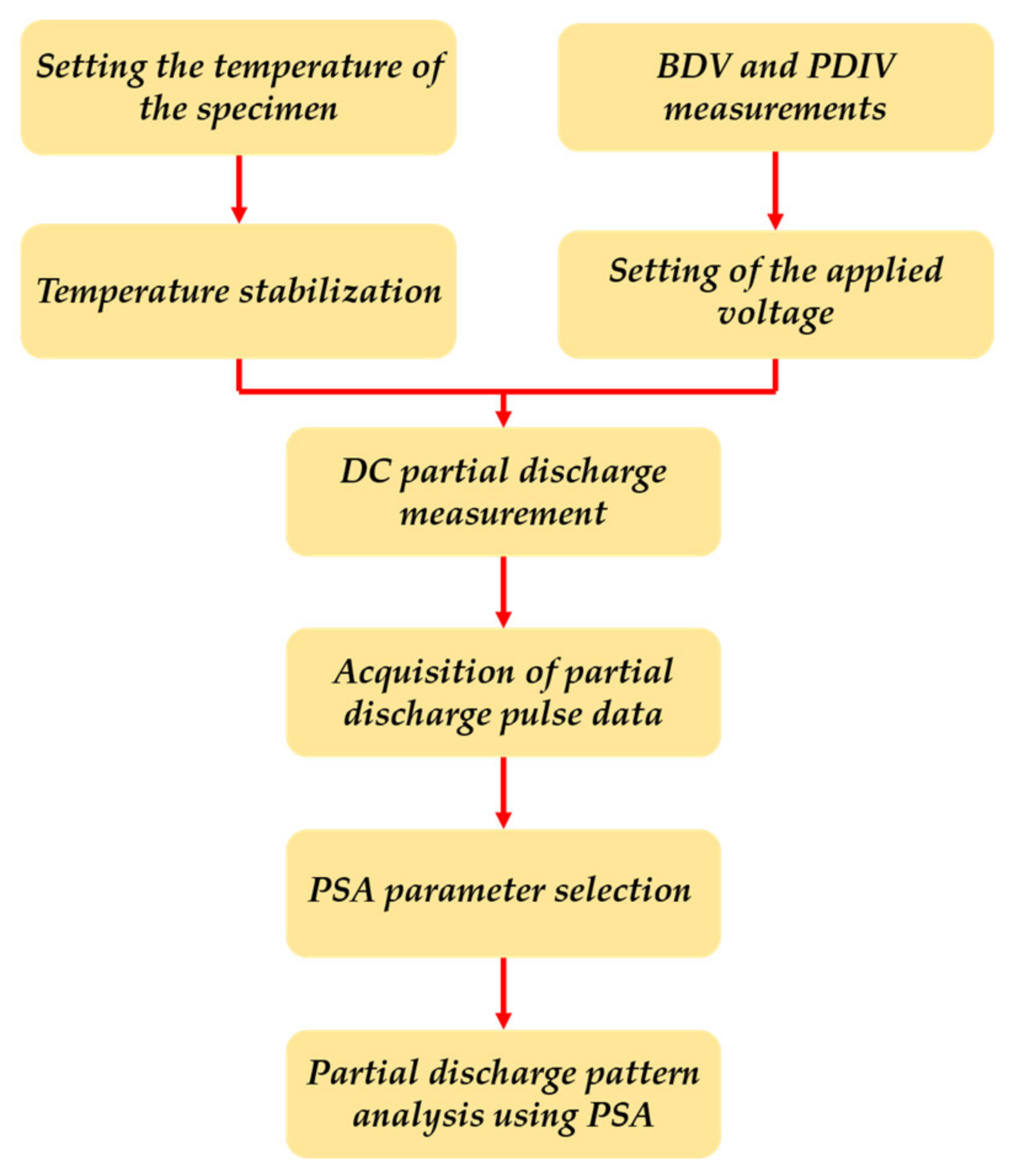
In the DC steady state, since the electric field has a resistive electric field distribution depending on the electrical conductivity, the DC partial discharge has different characteristics depending on temperature and applied voltage. Therefore, in this paper, the DC void discharges in MI-PPLP were measured according to the temperature of specimens and the magnitude of the applied voltage. The DC partial discharge pattern was obtained by the method shown in
Figure 4. In general, in order to acquire the pattern of DC partial discharge, the temperature of the specimen was set, temperature stabilization was performed,
BDV and
PDIV measurements were taken, and the applied voltage was set. Then, the partial discharge pulse data was acquired by measuring the DC partial discharge, and the partial discharge pattern was analyzed using the set PSA parameters.
In this paper, the method used to acquire the patterns of DC partial discharge is as follows. First, the temperature of the oil bath and oil circulation tank were set to 55 °C, 65 °C, and 75 °C and maintained for 1 h to equalize the temperature distribution of the oil and the specimen. Second, based on the experimental results of previous research [
38], the applied voltages according to the temperature of specimen were determined as the voltage between the lowest value of
BDV and the highest value of
PDIV. Then, the applied voltage for the void discharge was increased at the rising rate of 2 kV/s and maintained for at least 20 min to complete the polarization of the dielectric and formation of space charge. Finally, after analyzing the pulses of partial discharge measured for 1 h using PDMS, a pattern of void discharge was acquired using the PSA method.
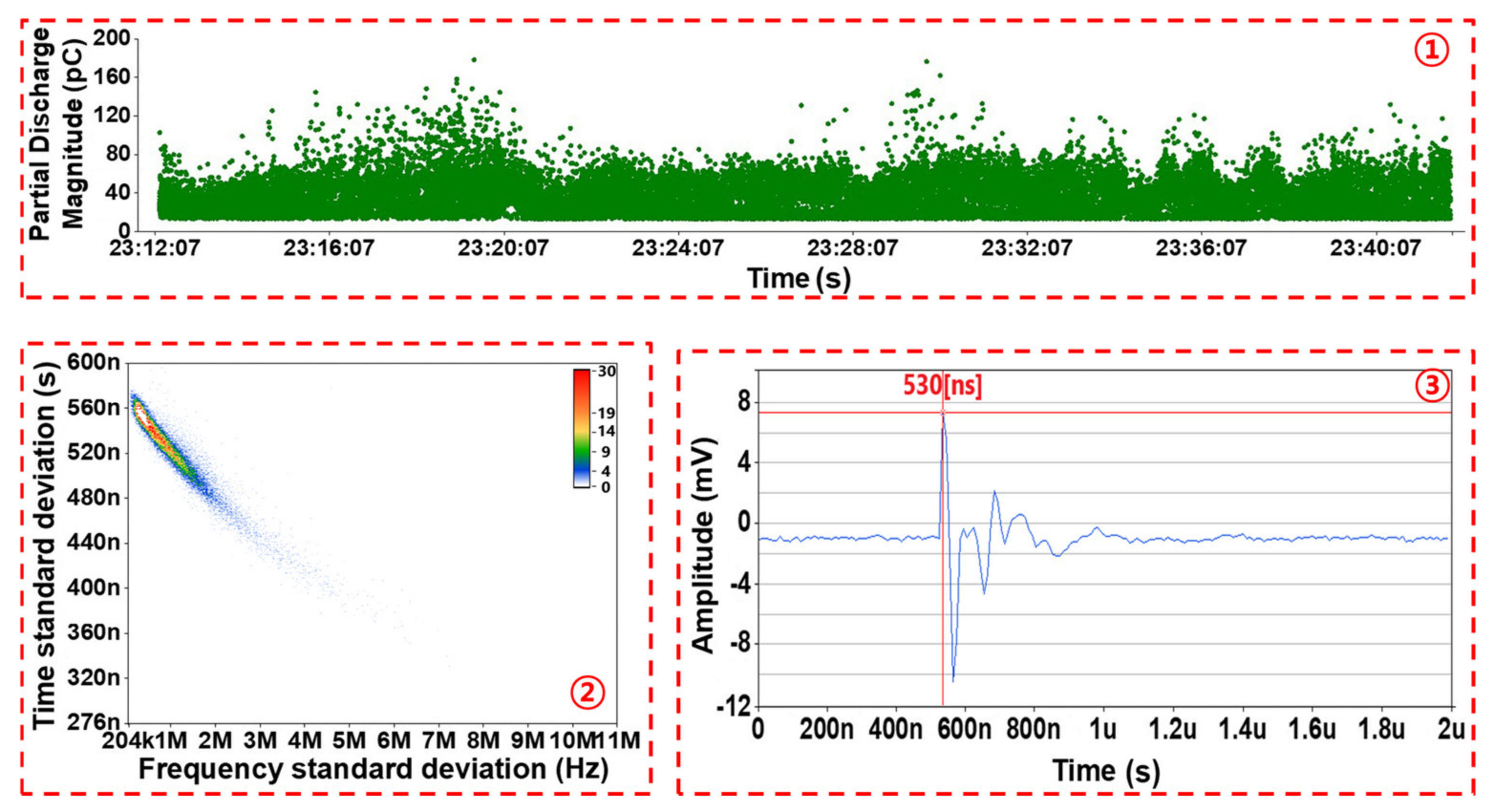
The PDMS device analyzes the partial discharge pulse by classifying it in four ways, as shown in
Figure 5. Zone ① records the occurrence time and magnitude of a partial discharge pulse in real time, from which the difference between occurrence time and magnitude of void discharge applied to the PSA can be obtained. Zone ② is a TF-map that shows the frequency standard deviation and time standard deviation of the partial discharge pulse, allowing for the partial discharge signal to be distinguished from the noise. Zone ③ shows the shape of partial discharge pulses generated in real time, like an oscilloscope.
The experimental method used for the analysis of the DC void discharge pattern due to long-term insulation aging is the same as the above-mentioned experimental method, and the measurement proceeds until dielectric breakdown occurs in the specimen.
2.4. DC Partial Discharge Pattern Analysis Using the Pulse Sequence Analysis
In the partial discharge analysis method developed over the past several decades, the analysis method by statistics has been used because partial discharge is simply recognized as a probabilistic process. Prof. Rainer Patsch thought that the partial discharge phenomenon was more affected by the deterministic process, and proposed a method to consider the mutual correlation of successive partial discharge pulses [
41]. This method is advantageous for the study of partial discharge phenomena in different defects by analyzing the correlation between successive pulses because the space charge remaining due to the influence of the previous pulse has a strong relationship with the generation of the subsequent pulse.
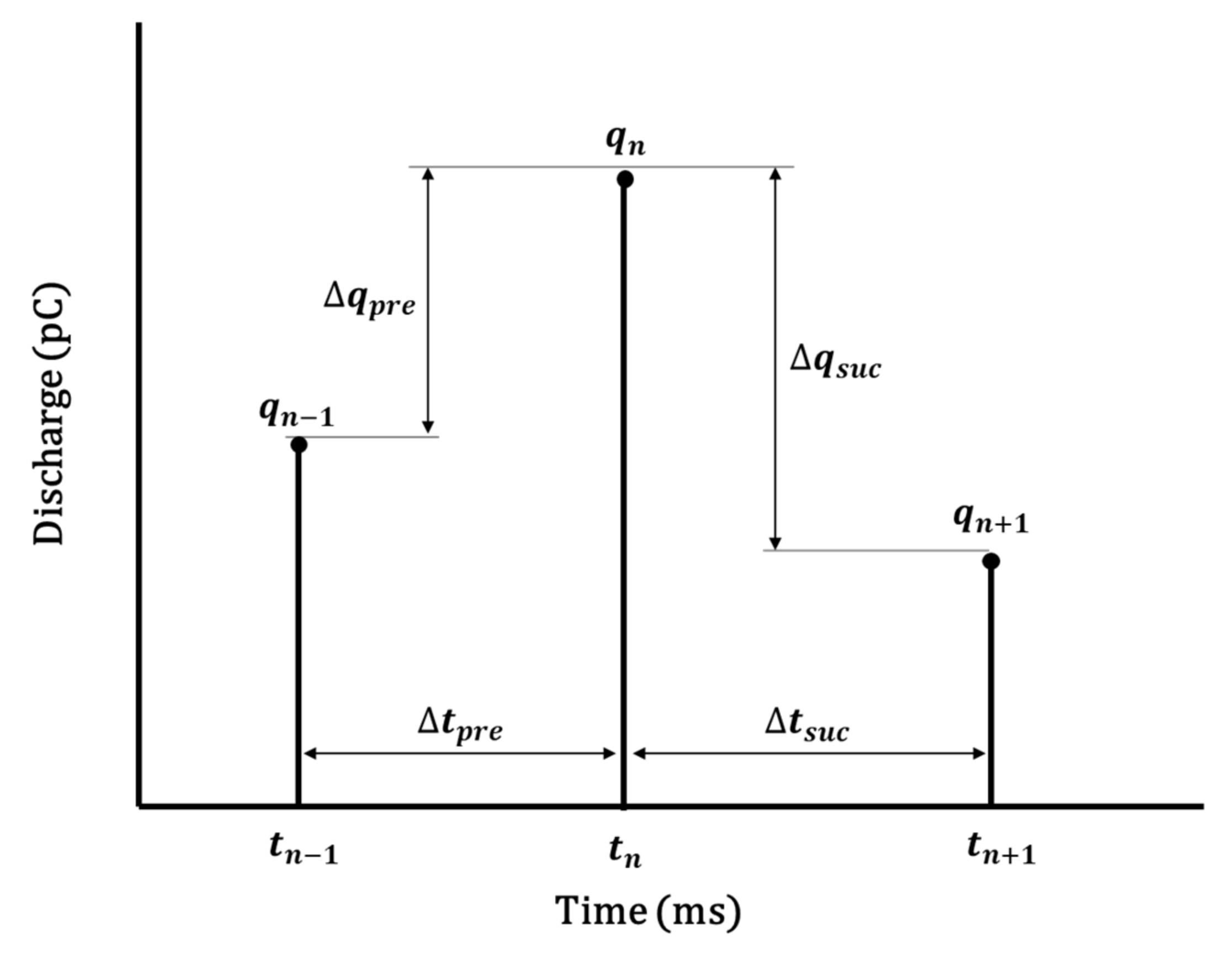
Since DC voltage has no phase information, it is impossible to use the PRPD pattern analysis method applied to AC voltage. Therefore, it is appropriate to perform insulation diagnosis of HVDC MI-PPLP cables using PSA, a method for analyzing the correlation between sequentially generated pulses. The PSA method uses a technique to analyze the correlation between the previous and successive discharge pulses to verify the space charge effect caused by the previous discharge pulse. The main parameters used in the PSA are the time difference between discharges (
) and the magnitude difference between discharges (
), as shown in
Figure 6.
The DC partial discharge pattern classification using the PSA uses the following methods.
Magnitude of discharge (q) vs. previous time difference ()
Magnitude of discharge (q) vs. successive time difference ()
Previous time difference () vs. successive time difference ()
Previous discharge difference () vs. successive discharge difference ()
In this paper, to acquire the DC void discharge pattern for HVDC MI-PPLP cable, the previous discharge difference () vs. successive discharge difference () method was used. In addition, the number of void discharges was shown through the change of color.
3. Results and Discussions
3.1. DC Void Discharge Measurement According to the Specimen Temperature and the Magnitude of Applied Voltage
The partial discharge of DC voltage has different repetition rates and discharge magnitude depending on the temperature of the specimen and the magnitude of the applied voltage. Therefore, the temperatures of the specimen were set at 55 °C, 65 °C, and 75 °C based on the operating temperature of HVDC MI-PPLP cable, and the magnitudes of the applied voltage were set based on the results of previous experiments.
In our previous paper [
38], when the temperatures of the specimen were set at 55 °C, 65 °C, and 75 °C, the average values of
DC PDIV and
DC BDV were measured, and the experimental results are shown in
Table 1. Based on the experimental results, to measure the void discharge according to the magnitude of the applied voltage, the applied voltages were set as 25 kV, 30 kV, and 35 kV, which are between the lowest value of
BDV and the highest value of
PDIV.
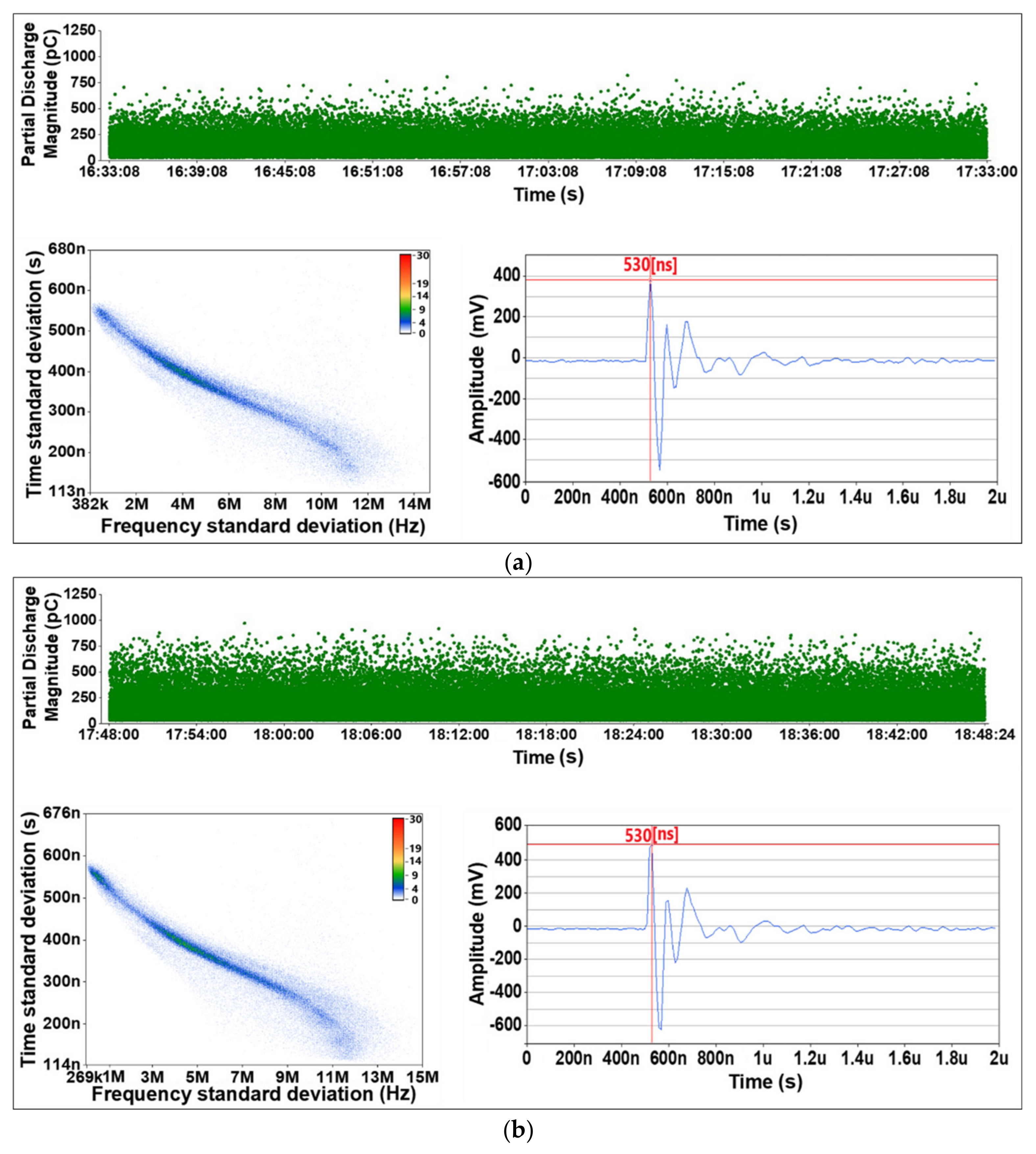
DC void discharges were measured for 1 h depending on the specimen temperature and the magnitude of the applied voltage, and typical experimental results measured by PDMS are shown in
Figure 7.
Figure 7 shows the measurement results of DC void discharge according to the temperature of the specimen for an applied voltage of 35 kV.
To confirm the consistency of each DC void discharge measurement, the frequency standard deviation and time standard deviation of the void discharge were compared using a TF map. At a temperature of 55 °C, the time standard deviation of void discharge ranged from 113 ns to 560 ns and the frequency standard deviation ranged from 382 kHz to 10 MHz. At a temperature of 65 °C, the time standard deviation of void discharge ranged from 114 ns to 560 ns, and the frequency standard deviation ranged from 269 kHz to 11 MHz. Finally, at a temperature of 75 °C, the time standard deviation and frequency standard deviation of the void discharge ranged from 102 ns to 560 ns and from 257 kHz to 12 MHz, respectively. TF mapping for each DC void discharge indicated that similar colonies with a long tail shape were formed in a 225-degree orientation. From the results of TF mapping, it was confirmed that the pulses of partial discharge stored in the PDMS occurred in the same void defect. In addition, it was confirmed that the standard deviation of the frequency of the DC void discharge pulse increased as the temperature of the specimen was increased.
The average magnitude of DC void discharges and number of DC void discharges for each set of experimental conditions are summarized in
Table 2. As the specimen temperature and applied voltage increased, the magnitude of the void discharges and the number of void discharges increased.
When the magnitude of the applied voltage increased, the voltage across the void increased due to the acceleration of the charge transfer speed, and eventually the magnitude of the void discharges and the number of void discharges increased.
As the specimen temperature increased, the thermionic emission from the electrode and the conductivity of MI-PPLP increased. Therefore, due to the increased number of charges and the concentration of the electric field inside the void, electron avalanche and progress of streamer inside the void were accelerated, and eventually the magnitude of void discharges and the number of void discharges increased.
3.2. DC Void Discharge Pattern Analysis Depending on the Specimen Temperature and the Magnitude of Applied Voltage
The method of pattern acquisition is summarized as follows. Firstly, the DC void discharge pulse data acquired through the HFCT sensor were accumulated in real time. Secondly, to remove the noise included in the DC void discharge data, trigger level reset and TF mapping of the DC void discharge data were conducted. Third, based on the TF mapping results, the DC void discharge pattern was analyzed using the previous discharge difference (=) vs. successive discharge difference (=) method, one of the PSA methods. Finally, the patterns acquired through the PSA method were plotted using the PYTHON program.
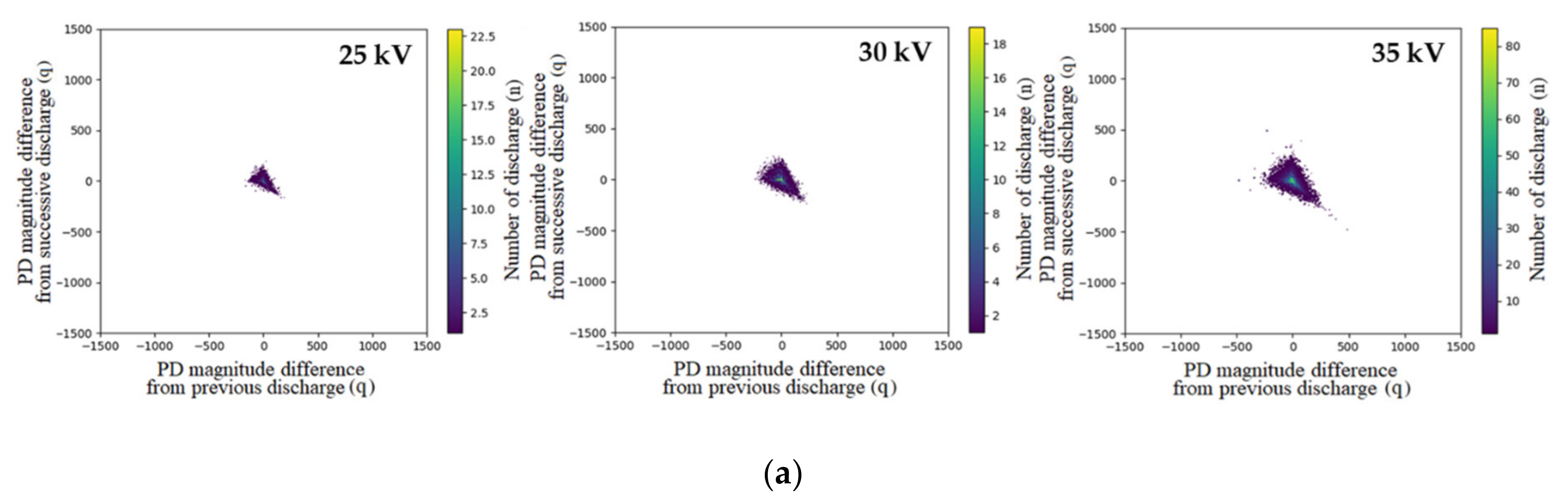
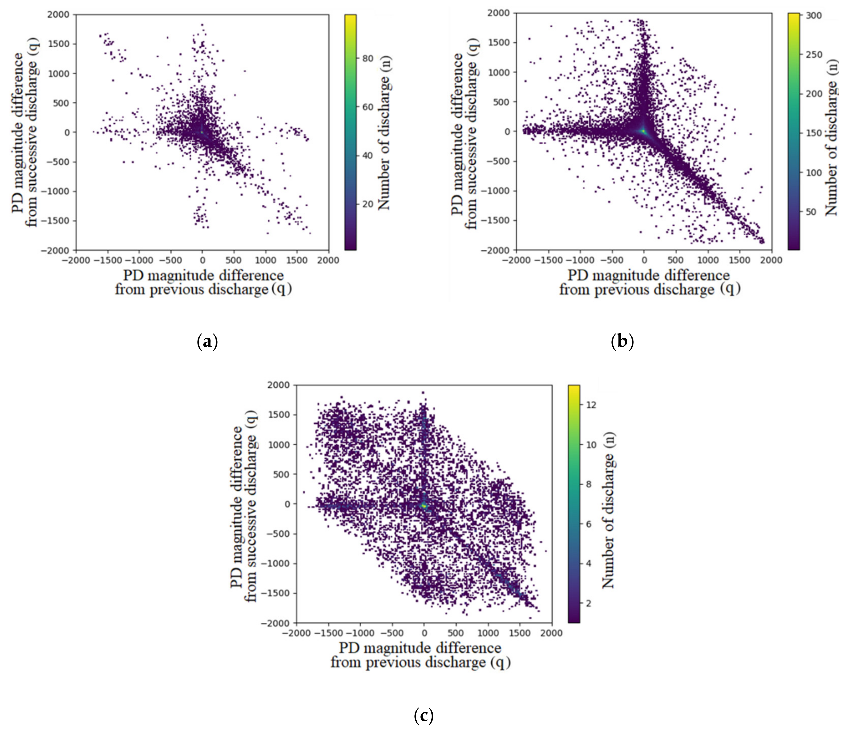
The DC void discharge patterns according to the temperature of the specimen and the magnitude of the applied voltage plotted through the PYTHON program are shown in
Figure 8 and summarized in
Table 3. The X-axis of the pattern represents the partial discharge (PD) magnitude difference from the previous discharge, and the Y-axis represents the PD magnitude difference from successive discharges. In addition, the number of void discharges is indicated through color change, with reference to the color bar on the right.
In DC void discharge, the magnitude of the discharge differs according to the residual voltage and the statistical time lag of the void discharge [
33]. Therefore, when pattern analysis is performed using the previous discharge difference (
=
) vs. successive discharge difference (
=
) method, the pattern is widely distributed.
In
Figure 8, it was confirmed that as the temperature of the specimen and the magnitude of the applied voltage increased, the size of the pattern increased for the same reason as mentioned in
Section 3.1. However, the shape of each pattern and TF-mapping results were very similar regardless of the experimental conditions as shown in
Table 3. The shape of the pattern was triangular, based on the capital letter Y, with the void discharge concentrated at the origin.
3.3. DC Void Discharge Measurements According to the Long-Term Insulation Aging
When a DC voltage higher than
PDIV was applied to the void that formed inside the butt-gap due to cavitation in the MI-PPLP cable, DC void discharge occurred in the void defect. If the DC void discharge persisted, the electrical and thermal aging of the MI-PPLP accelerated, and eventually dielectric breakdown occurred due to the lowering of dielectric strength. Therefore, to prevent dielectric breakdown due to insulation aging in HVDC MI-PPLP cables, a technology that can detect insulation aging of MI-PPLP in advance is required. In this section, DC void discharge was measured continuously until dielectric breakdown occurred to confirm the pre-symptoms of dielectric breakdown of MI-PPLP due to DC void discharge. The temperature of the specimen and the magnitude of the applied voltage were set at 75 °C and 35 kV, respectively, which were the maximum temperature and maximum voltage tested in
Section 3.
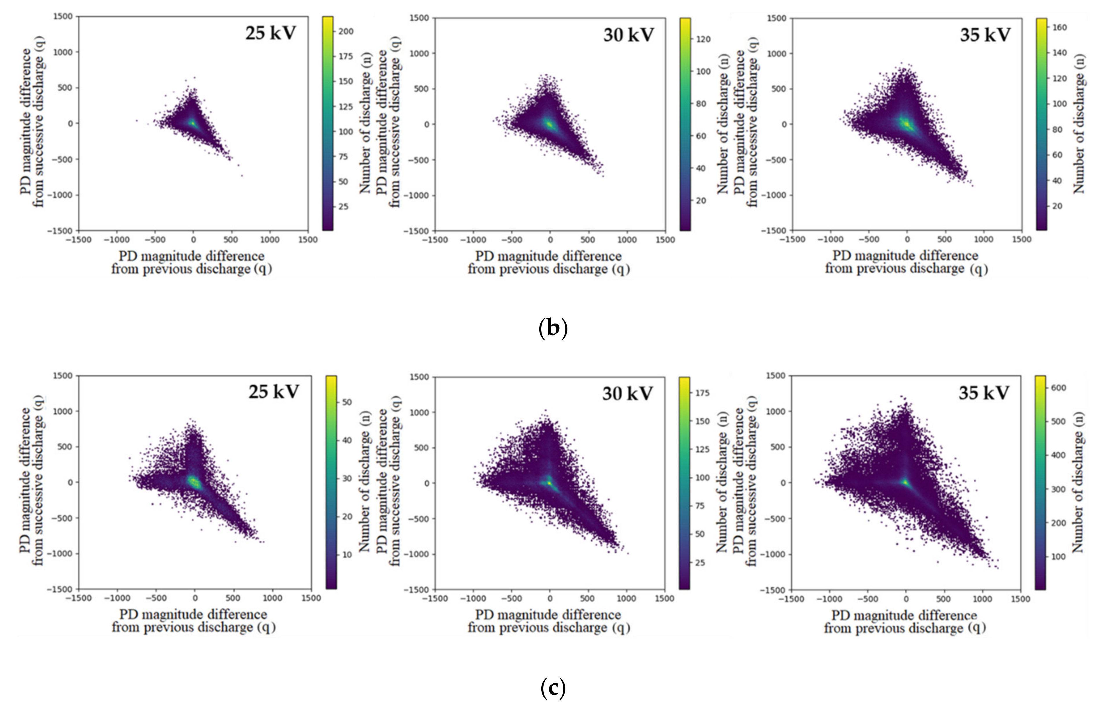
Dielectric breakdown occurred 60 h after the DC voltage was first applied, and the magnitude of the discharge over time and the TF map are shown in
Figure 9a. Results of the experiment indicated that for about 26 h after the voltage was first applied, the magnitudes of the DC void discharge were measured to range from about 0 to 1000 pC, and after 26 h of applying the voltage, the magnitudes of the DC void discharge were measured to range from about 0 to 2000 pC. As a result of TF mapping for each DC void discharge, it was confirmed that a long tail-shaped colony was formed in the 225-degree orientation, as shown in
Figure 7, and a new colony other than void discharge was additionally formed. Therefore, based on the TF map, the accumulated partial discharges were classified into two groups, and the generation time and magnitude of the void discharges were compared, as shown in the pink box in
Figure 9b,c.
As a result of TF mapping for the blue box in
Figure 9b, the time standard deviation was 160 ns~600 ns and the frequency standard deviation was 279 kHz–24 MHz, which was identified as a void discharge colony similar to that of
Figure 7. In addition, as shown in the pink box, the magnitudes of discharge were measured to be about 0–1000 pC from the time when DC voltage was applied until the dielectric breakdown occurred, and the magnitude of discharge slightly increased as the DC void discharge continued.
As a result of TF mapping for the red box in
Figure 8c, the time standard deviation and frequency standard deviation were measured as 95–160 ns and 8–20 MHz, respectively, which was confirmed as a new discharge colony different from the DC void discharge colony. In addition, as shown in the pink box, the magnitudes of the discharge were measured to be about 500–2000 pC from 26 h after the start of voltage application until dielectric breakdown occurred, and the magnitude of discharge increased slightly as the DC void discharge continued. If void discharge continues, insulation aging occurs at the interface between the void and MI-PPLP [
16,
23], and eventually the magnitudes of discharge increase due to the lowering of dielectric strength. Therefore, from these results, insulation aging occurred from about 26 h after the start of voltage application, and a new discharge occurred due to insulation aging of MI-PPLP.
3.4. DC Void Discharge Pattern Analysis According to the Long-Term Insulation Aging Classified Through TF Map
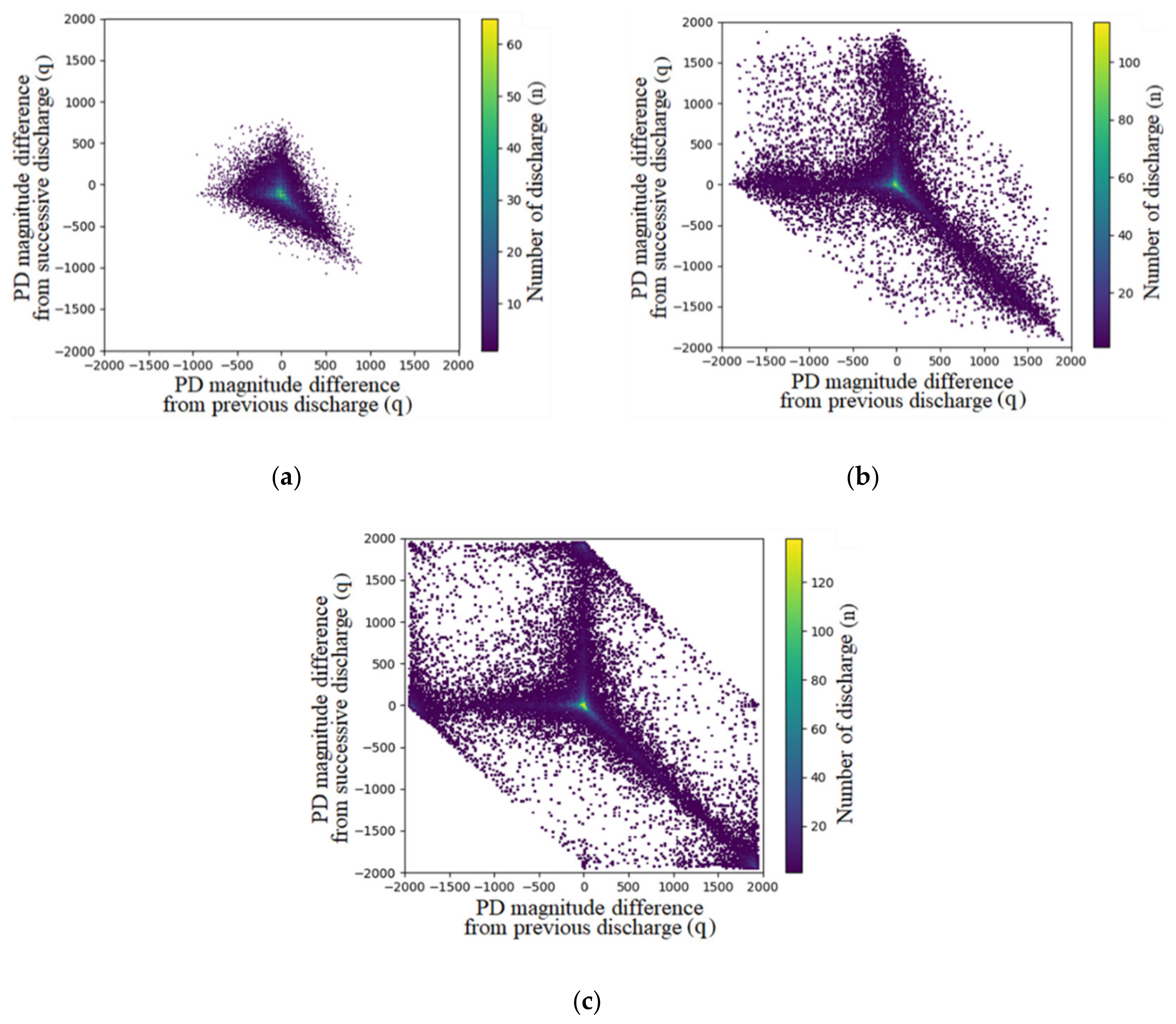
To obtain patterns of DC void discharge due to long-term insulation aging, pulse data of DC void discharge from the start of discharge to the occurrence of dielectric breakdown were analyzed. The pattern acquisition sections were classified into the initial discharge occurrence, the beginning of insulation aging, and before the dielectric breakdown, and the patterns were acquired based on the data accumulated for one hour in each of the pattern acquisition sections.
Firstly, pattern analysis was performed on the measurements of long-term DC void discharge on which TF mapping was not performed, as shown in
Figure 9a, and the pattern analysis results are shown in
Figure 10.
Figure 10a represents the pattern in the initial discharge generation section of the long-term DC void discharge experiment; a triangular pattern based on the capital letter Y in which the void discharge is concentrated at the origin was acquired. This pattern has the same shape as that of the void discharge obtained in
Figure 8.
Figure 10b shows the pattern at the beginning of the insulation aging section, which shows a shape with a faint hexagonal form added to the existing void discharge pattern. This pattern is considered to be caused by a sharp increase in the magnitude of the discharge due to insulation aging.
Figure 10c represents the pattern in the section before the dielectric breakdown, which shows a more pronounced hexagonal pattern than does
Figure 10b.
Secondly, pattern analysis was performed on the discharge colony classified as void discharge through TF mapping, as shown in
Figure 9b, and the result is shown in
Figure 11.
Figure 11a–c represents the patterns in the sections classified as initial discharge occurrence, beginning of insulation aging, and before the dielectric breakdown, respectively. The shapes of all patterns were the same as that of void discharge. From these results, it was confirmed that void discharge occurred continuously inside the void defect regardless of the insulation aging of MI-PPLP.
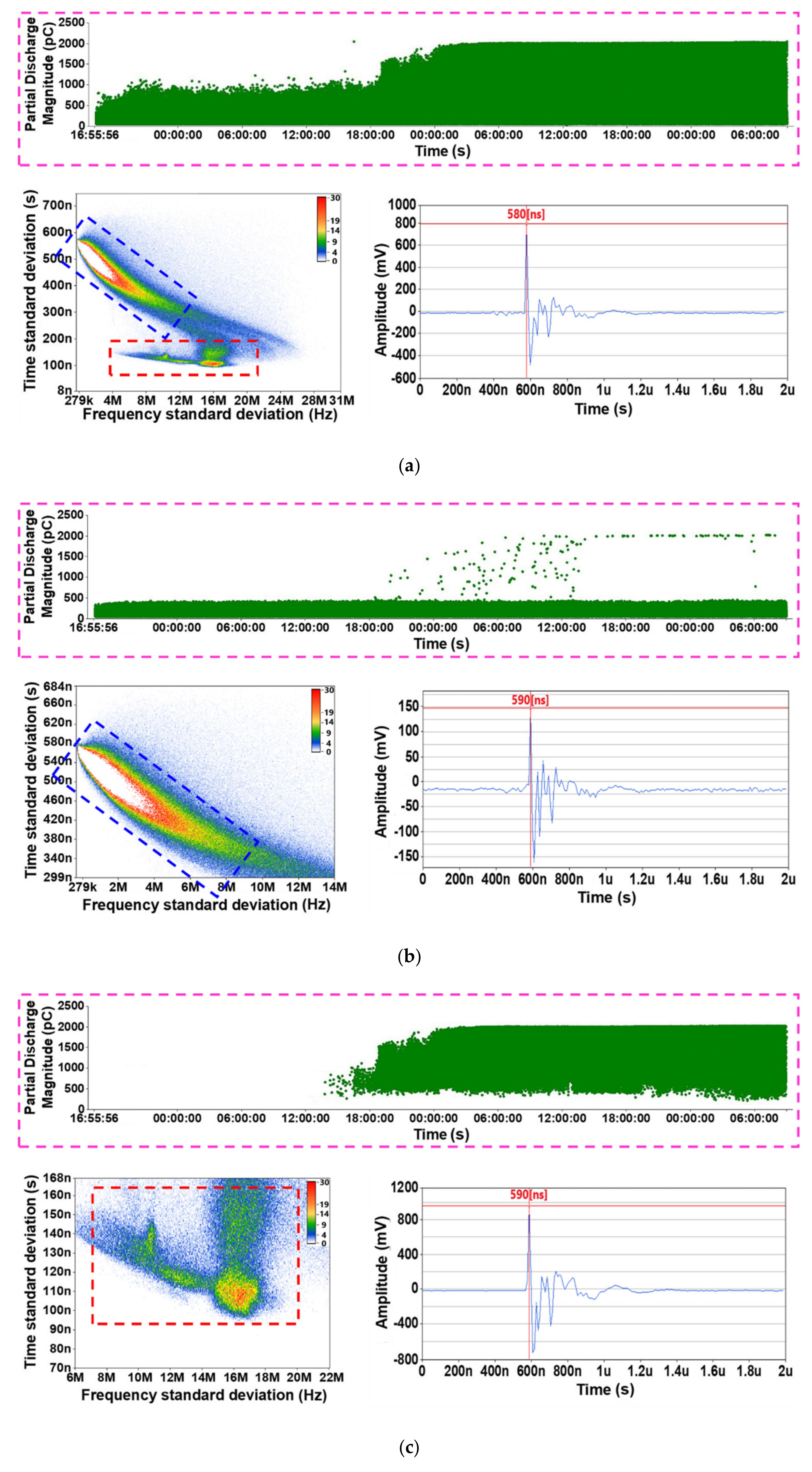
Finally, pattern analysis was performed on the discharge colony classified as void discharge due to insulation aging of MI-PPLP through TF mapping, as shown in
Figure 9c, and the result is shown in
Figure 12. The DC void discharges caused by the insulation aging of MI-PPLP were generated from the beginning of insulation aging.
Figure 12a shows the pattern at the beginning of insulation aging, which has a hexagonal star shape.
Figure 12b shows the pattern from the middle section of the insulation aging, which has a more pronounced hexagonal shape compared to
Figure 12a.
Figure 12c shows the pattern in the section before the dielectric breakdown, which shows a complete hexagonal shape. From these results, it was confirmed that insulation aging was accelerated due to continuous DC void discharge at the interface between void and MI-PPLP, and eventually a new discharge pattern appeared due to the decrease in dielectric strength. In addition, it was confirmed that with increasing insulation aging of the MI-PPLP due to DC void discharge, the hexagonal shape pattern became more and more distinct.
DC void discharge characteristics and patterns according to the long-term insulation aging classified through TF mapping are summarized in
Table 4. Through pattern analysis, it was confirmed that the causes of the two discharge colonies classified by TF mapping in
Section 3.3 are different. In addition, it was confirmed that when the insulation aging occurred in the specimen due to continuous DC void discharge, a new hexagonal discharge pattern was observed instead of the existing void discharge pattern. Therefore, if the DC void discharge patterns due to insulation aging of MI-PPLP obtained in this section were founded during the insulation diagnosis process of the MI-PPLP cable, it can be determined that pre-symptoms of the dielectric breakdown of MI-PPLP cable due to insulation aging have occurred. However, to apply the insulation diagnosis technology through pattern analysis to the operating MI-PPLP cable, additional noise analysis must be performed depending on the surrounding environment and operating conditions.
4. Conclusions
In this paper, in order to propose an insulation diagnosis method for void defects in HVDC MI-PPLP cable, DC void discharge patterns were obtained according to the magnitude of applied voltage and temperature of the specimen. In addition, by analyzing the DC void discharge patterns until insulation breakdown occurred in the MI-PPLP specimen due to the long-term void discharge, the DC void discharge patterns according to the progress of insulation aging were analyzed. In addition, by applying TF mapping to the PSA method currently used as a pattern analysis method for DC partial discharge, new discharge patterns according to insulation deterioration were obtained.
The results derived from this study are as follows.
TF mapping for DC void discharge in MI-PPLP indicated that similar colonies with a long tail shape were formed in the 225-degree orientation despite the different experimental conditions.
As the specimen temperature and the magnitude of the applied voltage increased, the size of the pattern increased, but the pattern retained the triangular shape based on the capital letter Y, with the void discharge concentrated at the origin.
As a result of TF mapping for long-term DC void discharge in MI-PPLP, a new colony was formed due to insulation aging at the interface between the void and MI-PPLP due to continuous DC void discharge.
In the pattern analysis for the colony classified as void discharge caused by insulation aging of MI-PPLP through TF mapping, a hexagonal pattern different from the existing void discharge pattern was obtained.
Through the patterns of DC void discharge obtained in this paper, it is possible to identify void defects in HVDC MI-PPLP cables. In addition, based on the DC void discharge patterns after long-term insulation aging, it can be applied to the insulation diagnosis and maintenance of the cable by recognizing in advance the pre-symptoms of dielectric breakdown of the HVDC MI-PPLP cable.
In the future, various patterns obtained through this paper will be applied to the MI-PPLP model cable to verify the consistency of the experimental results. In addition, it will be applied to the Bukdangjin-Goduk (South Korea, ±500 kV MI-PPLP cable) project to perform insulation diagnosis and maintenance of HVDC MI-PPLP cables. Additionally, the partial discharge pattern analysis method performed in this paper can be applied to other DC electric power devices. However, since DC partial discharge is affected by electrical conductivity, temperature, electrode shape, etc., additional experiments are required to apply the experimental results in the paper to other DC electric power devices.


