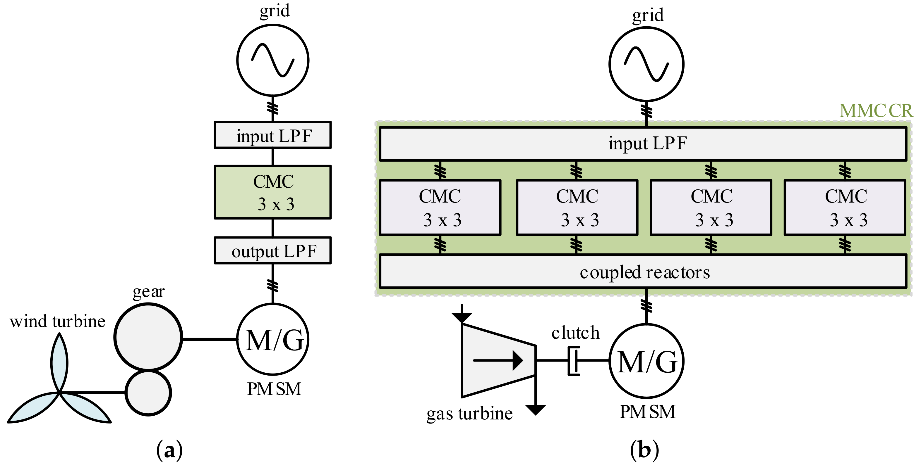
Figure 1.
Examples of simplified application diagrams of turbines: (a) a wind turbine with a gear, (b) a gas turbine with a clutch. Conventional Matrix Converter (CMC) 3 × 3—conventional matrix converter with 3 inputs and 3 outputs, M/G—motor/generator, LPF—low-pass filter.
Figure 1.
Examples of simplified application diagrams of turbines: (a) a wind turbine with a gear, (b) a gas turbine with a clutch. Conventional Matrix Converter (CMC) 3 × 3—conventional matrix converter with 3 inputs and 3 outputs, M/G—motor/generator, LPF—low-pass filter.
Figure 2.
The simplified speed profile of the gas turbine: M—PMSM operates as a motor, G—PMSM operates as a generator, SVPWM—high-frequency modulation method based on the space-vector concept, Nearest Vector Modulation (NVM) and Pulse Width Modulation (PWR)—the low-switching frequency type of PWM modulation.
Figure 3.
The general discrete reference vector projection concept:
—voltage amplitude,
and
pulsations,
p a number of discrete voltage vectors [
7].
Figure 3.
The general discrete reference vector projection concept:
—voltage amplitude,
and
pulsations,
p a number of discrete voltage vectors [
7].
Figure 4.
Conventional matrix converter as a 3-pulse system: (a) schematic diagram, (b) the voltages discrete projection.
Figure 4.
Conventional matrix converter as a 3-pulse system: (a) schematic diagram, (b) the voltages discrete projection.
Figure 5.
Two conventional matrix converters make the 6-pulse system: (a) schematic diagram, (b) the voltages discrete projection.
Figure 5.
Two conventional matrix converters make the 6-pulse system: (a) schematic diagram, (b) the voltages discrete projection.
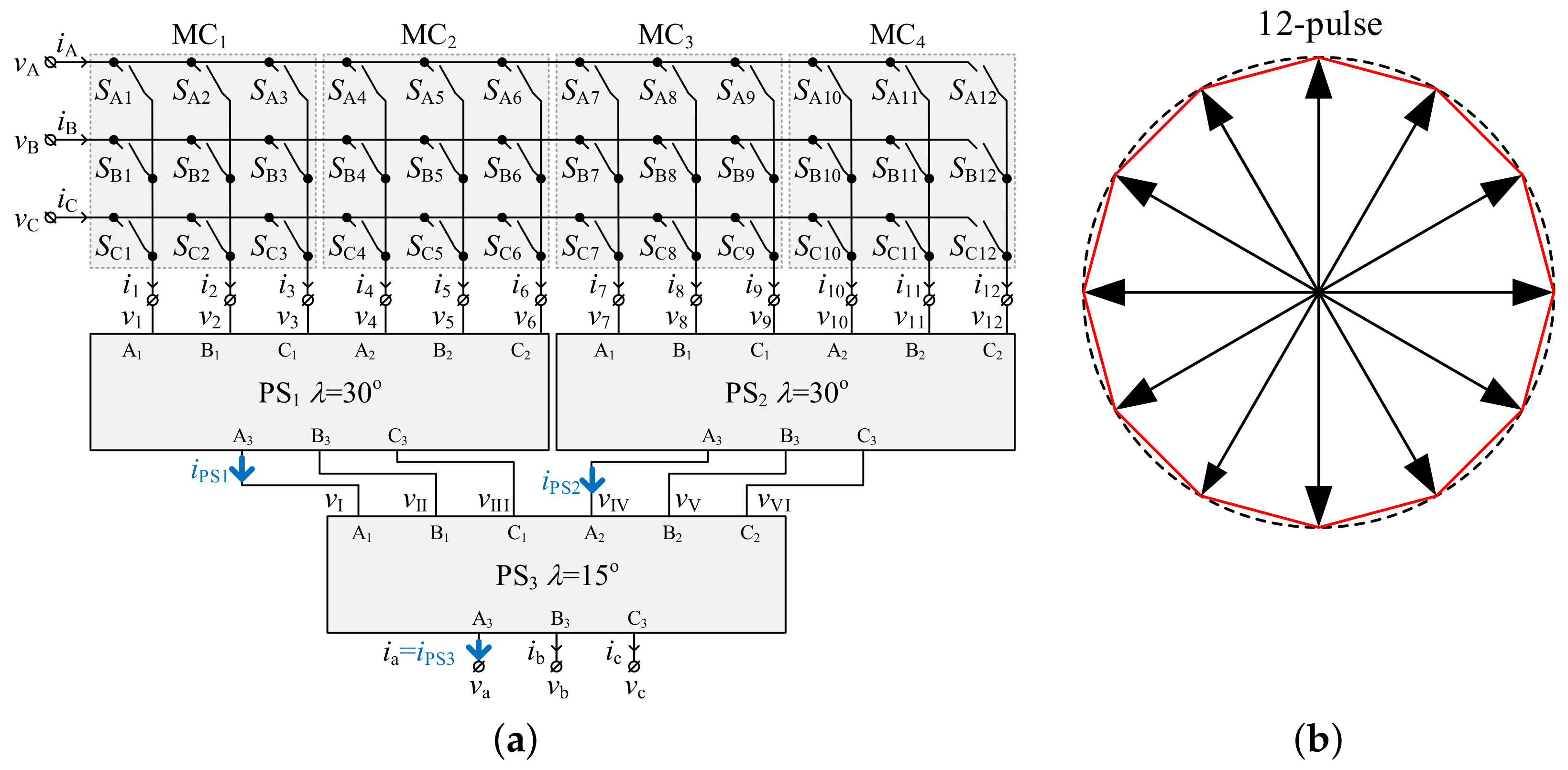
Figure 6.
Four conventional matrix converters make the 12-pulse system: (a) schematic diagram, (b) the voltages discrete projection.
Figure 6.
Four conventional matrix converters make the 12-pulse system: (a) schematic diagram, (b) the voltages discrete projection.
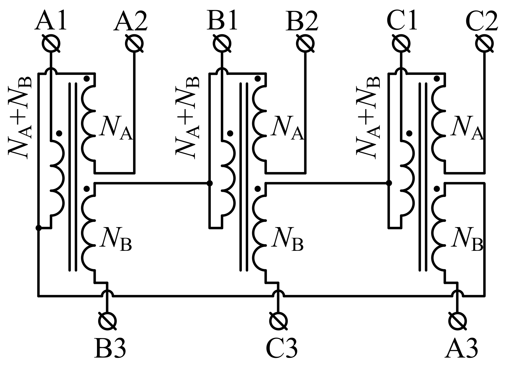
Figure 7.
Phase Shifter schematic.
Figure 7.
Phase Shifter schematic.
Figure 8.
The space-vector diagram for switch states.
Figure 8.
The space-vector diagram for switch states.
Figure 9.
The space-vector diagram for switch states.
Figure 9.
The space-vector diagram for switch states.
Figure 10.
The PWR modulation workspace for switch states.
Figure 10.
The PWR modulation workspace for switch states.
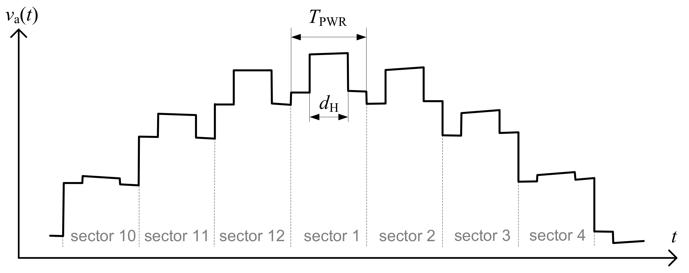
Figure 11.
Fragment of phase voltage waveform for the PWR modulation using the states.
Figure 11.
Fragment of phase voltage waveform for the PWR modulation using the states.
Figure 12.
An error rate, defined by (
21), for proposed NVM method:
,
,
.
Figure 12.
An error rate, defined by (
21), for proposed NVM method:
,
,
.
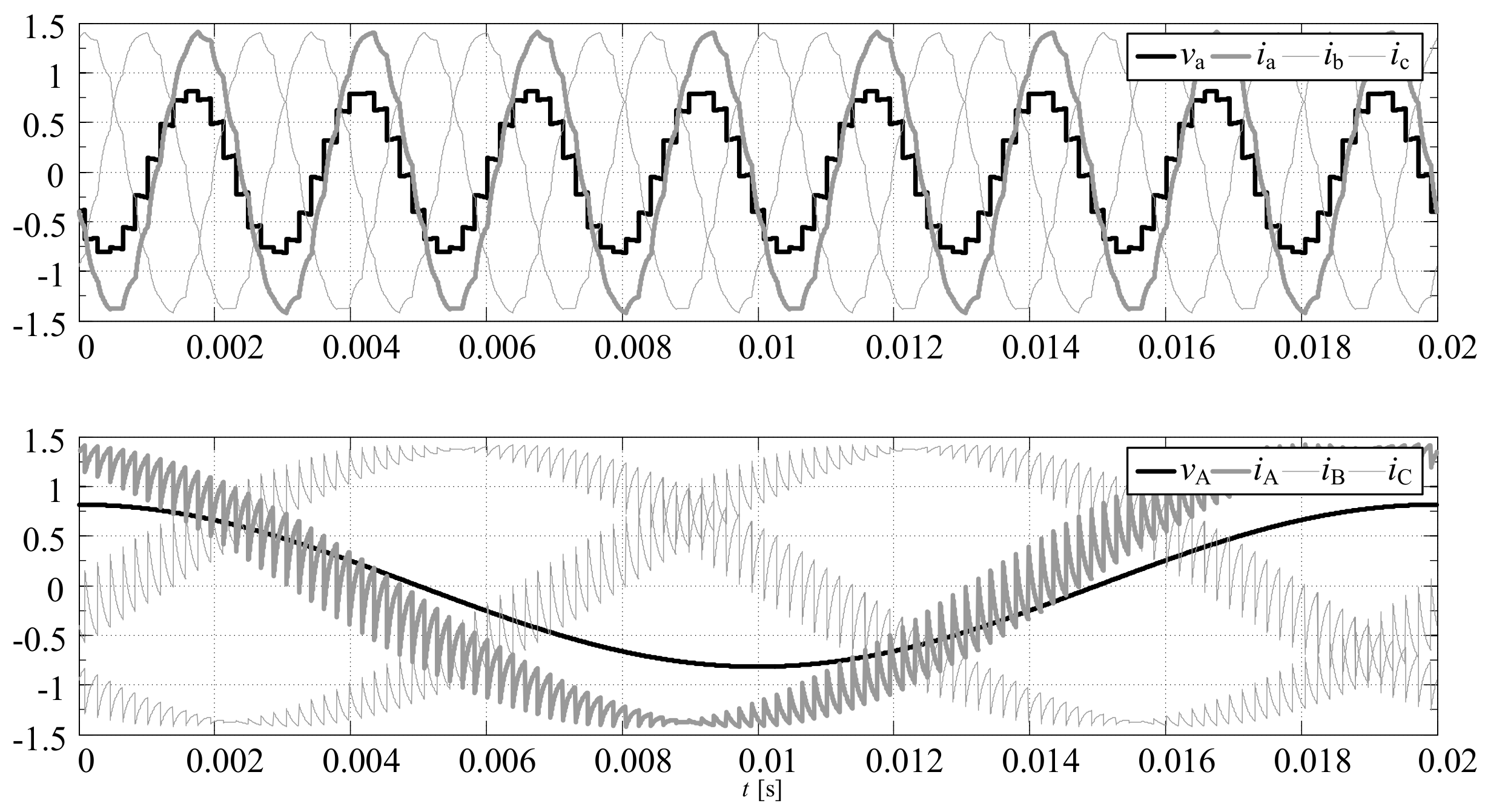
Figure 13.
The waveforms of the phase voltages and currents at the output and input of the PWR controlled MMCCR for the switch state sequences: load model-1, , , , .
Figure 13.
The waveforms of the phase voltages and currents at the output and input of the PWR controlled MMCCR for the switch state sequences: load model-1, , , , .
Figure 14.
The waveforms of the phase voltages and currents at the output and input of the PWR controlled MMCCR for the switch state sequences: load model-1, , .
Figure 14.
The waveforms of the phase voltages and currents at the output and input of the PWR controlled MMCCR for the switch state sequences: load model-1, , .
Figure 15.
The waveforms of the phase voltages and currents at the output and input of the PWR controlled MMCCR for the switch state sequences: load model-1, , .
Figure 15.
The waveforms of the phase voltages and currents at the output and input of the PWR controlled MMCCR for the switch state sequences: load model-1, , .
Figure 16.
The waveforms of the phase voltages and currents at the output and input of the PWR controlled MMCCR for the switch state sequences: load model-1, , .
Figure 16.
The waveforms of the phase voltages and currents at the output and input of the PWR controlled MMCCR for the switch state sequences: load model-1, , .
Figure 17.
The zoom of the rapid change of switch sequence type for PWR modulation and load model-2, , and .
Figure 17.
The zoom of the rapid change of switch sequence type for PWR modulation and load model-2, , and .
Figure 18.
The maximal relative magnetic flux F in PS coupled reactor in function of voltage transfer ratio q and output frequency ratio .
Figure 18.
The maximal relative magnetic flux F in PS coupled reactor in function of voltage transfer ratio q and output frequency ratio .
Figure 19.
Example output voltage waveforms, for NVM modulation, during gradually increasing the voltage gain q from 0.27 to 0.43 for .
Figure 19.
Example output voltage waveforms, for NVM modulation, during gradually increasing the voltage gain q from 0.27 to 0.43 for .
Figure 20.
The comparison of the PWR and NVM modulation methods during the inverter operation: (a) the load current total harmonic distortion in the applicable range of modulation index, (b) the load current RMS value comparison of reference and proposed modulation.
Figure 20.
The comparison of the PWR and NVM modulation methods during the inverter operation: (a) the load current total harmonic distortion in the applicable range of modulation index, (b) the load current RMS value comparison of reference and proposed modulation.
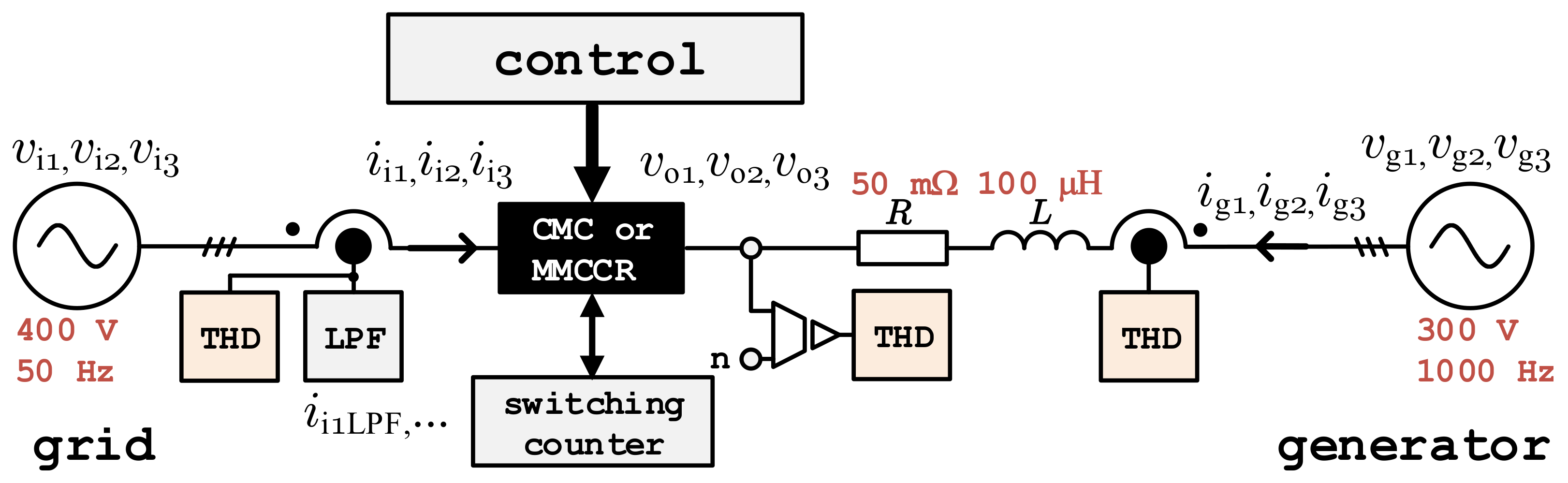
Figure 21.
A potential application scheme with a high-speed PMSM generator: CMC—conventional matrix converter, MMCCR—the proposed converter, THD—calculation of the total harmonic distortion block, LPF—the low–pass filter, and “n”—the star point for the phase voltage measurement.
Figure 21.
A potential application scheme with a high-speed PMSM generator: CMC—conventional matrix converter, MMCCR—the proposed converter, THD—calculation of the total harmonic distortion block, LPF—the low–pass filter, and “n”—the star point for the phase voltage measurement.
Figure 22.
The proposed control scheme: PLL—phase-locked loop, MMCCR—the proposed converter, PI—standard proportional integral controller, —grid’s voltage angle, —the synchronisations angle, —generator’s voltage angle, —an active reference current for generator, —a reactive reference current for generator, —for simplicity, mechanical pulsation is equal to electrical pulsation.
Figure 23.
The step change 0–200 A of the reference active generator current in s: (a) for CMC converter, (b) for MMCCR converter.
Figure 23.
The step change 0–200 A of the reference active generator current in s: (a) for CMC converter, (b) for MMCCR converter.
Figure 24.
The input current spectrums for both converters.
Figure 24.
The input current spectrums for both converters.
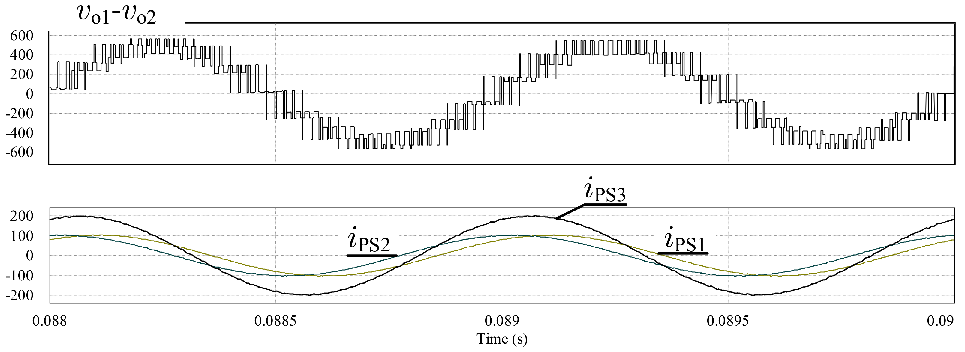
Figure 25.
Converter’s line–to–line output (correspond to
Figure 21) voltage and the current sharing among the PS shown in
Figure 6—SVPWM modulation.
Figure 25.
Converter’s line–to–line output (correspond to
Figure 21) voltage and the current sharing among the PS shown in
Figure 6—SVPWM modulation.
Figure 26.
MMCCR converter’ output voltage and the generator current for NVM modulation: % and %.
Figure 26.
MMCCR converter’ output voltage and the generator current for NVM modulation: % and %.
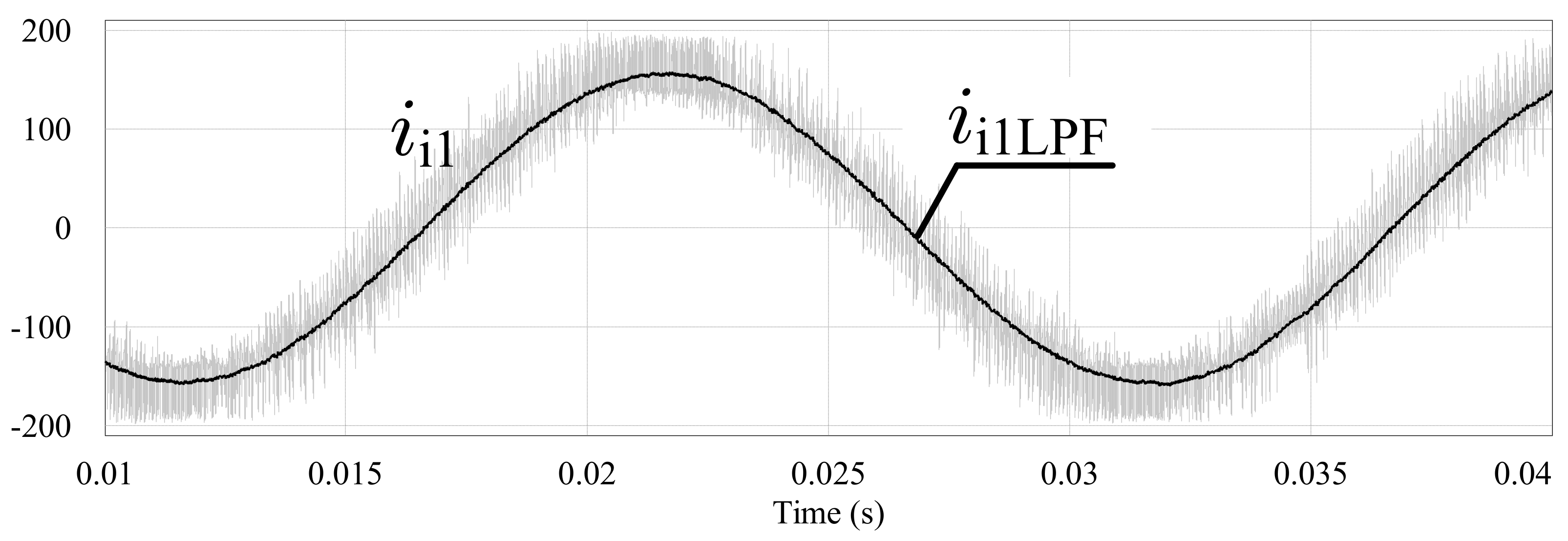
Figure 27.
An input current and its filtered waveform for NVM modulation: %.
Figure 27.
An input current and its filtered waveform for NVM modulation: %.
Table 1.
Turns number for shift angle equal to (conversion values).
Table 1.
Turns number for shift angle equal to (conversion values).
| <100 | <300 | <1000 |
|---|
| 15 | 56 | 209 |
| 15 | 56 | 209 |
Table 2.
Turns number for shift angle equal to (conversion values).
Table 2.
Turns number for shift angle equal to (conversion values).
| <100 | <300 | <1000 |
|---|
| 41 | 153 | 571 |
| 15 | 56 | 209 |
Table 3.
Allowed switch states.
Table 3.
Allowed switch states.
| | States | |
|---|
| | |
| | |
Table 4.
Allowed switch states.
Table 4.
Allowed switch states.
| | States | |
|---|
| | |
| | |
Table 5.
Example the switch states sequences in the first 3 sectors.
Table 5.
Example the switch states sequences in the first 3 sectors.
| Type | | Sector 1 | Sector 2 | Sector 3 |
|---|
| 571/209 | V55–V0–V55 | V9–V1–V9 | V4–V10–V4 |
| 571/209 | V29–V0–V29 | V18–V2–V18 | V8–V20–V8 |
Table 6.
20 kVA/400 V load models simulation parameters.
Table 6.
20 kVA/400 V load models simulation parameters.
| | R [] | L [H] | Z [] | PF |
|---|
| model-1 | 7.75 | 0.0008 | 8.0 | 0.97 |
| model-2 | 4 | 0.0028 | 8.0 | 0.5 |
Table 7.
Comparison of load current THD and average switching frequency for PWR modulation using the switch state sequences and .
Table 7.
Comparison of load current THD and average switching frequency for PWR modulation using the switch state sequences and .
| | Switch State Type |
|---|
| q | 0.732 | 0.75 | 0.8 | 0.85 | 0.9 | 0.95 | 1 |
| THD [%] | 3.15 | 3.35 | 4.8 | 5.4 | 5.2 | 4.3 | 3.1 |
| [Hz] | 1350 | 3125 | 3125 | 3125 | 3125 | 3125 | 450 |
| | Switch State Type |
| q | 0.732 | 0.75 | 0.8 | 0.85 | 0.9 | 0.95 | 1 |
| THD [%] | 4.15 | 4.6 | 6.2 | 7.0 | 6.5 | 5.5 | 4.1 |
| [Hz] | 1050 | 2450 | 2450 | 2450 | 2450 | 2450 | 350 |
Table 8.
Selected results of the comparison CMC and MMCCR converters during SVPWMmodulation.
Table 8.
Selected results of the comparison CMC and MMCCR converters during SVPWMmodulation.
| Converter Type | | | | The Relative Number of Switching Operations |
|---|
| CMC | 74% | 73% | 1.6% | 100% |
| MMCCR | 28% | 26% | 0.85% | ≃50% |


 ,
, 


