Abstract
This article presents three variants of the Pulse Width Modulation (PWM) for the Double Square Multiphase type Conventional Matrix Converters (DSM-CMC) supplying loads with the open-end winding. The first variant of PWM offers the ability to obtain zero value of the common-mode voltage at the load’s terminals and applies only six switches within the modulation period. The second proposal archives for less Total Harmonic Distortion (THD) of the generated load voltage. The third variant of modulation concerns maximizing the voltage transfer ratio, minimizing the number of switching, and the common-mode voltage cancellation. The discussed modulations are based on the concept of sinusoidal voltage quadrature signals, which can be an effective alternative to the classic space-vector approach. In the proposed approach, the geometrical arrangement of basic vectors needed to synthesize output voltages is built from the less number of vectors, which is equal to the number of the matrix converter’s terminals. The PWM duty cycle computation is performed using only a second-order determinant of the voltages coordinate matrix without using trigonometric functions. A new approach to the PWM duty cycles computing and the load voltage synthesis by 5 × 5 and 12 × 12 topologies has been verified using the PSIM simulation software.
1. Introduction
A fully controlled bidirectional semiconductor switch is an element of the Conventional Matrix Converter (CMC) which offers a direct AC–AC voltages conversion with additional input power factor control functionality. This type of converter, in comparison with the more established Voltage Source Inverter (VSI), has certain individual features that determine the innovation of such a solution [,,]. It does not contain a bulk dc-link capacitor, thus is far more promising in terms of power density with the inherent four-quadrant operation [,]. Compared to traditional variable speed drives with CMC, the multi-phase electric motor drive gives some fundamental advantages. These configurations have grater system redundancy because it can operate during some fault conditions, is characterized by the lower torque ripple and lower per-leg converter rating []. Furthermore, the operation of multiphase motors is quieter, allowing for the independent control of two or more series/parallel connected motors []. Multiphase electric machines can be fed also by the conventional matrix converter with three inputs [,,,]. The matrix topology is also presented as a unit, which control the power flow between the power generator and the electrical grid [,,,,]. Multiphase generators have also been used in systems generating electricity such as offshore installations and wind farms [,]. Another application of the multiphase matrix converter in straight forward energy conversion is described in [], where the 6 × 6 CMC and multi-winding transformer have been used to supply variable reactive power flow to the power system. A modulation approach based on the model of the 5 × 5 matrix converter with fictitious DC-link was shown in conference paper [].
Multi-phase electric machines, including three-phase and five-phase variants, can be designed as a machine with open stator winding. Such a solution, especially in combination with a CMC, offers some important features. First, the possibility of direct power supply to both ends of the stator phase winding increases the maximum voltage amplitude within the linear range of the PWM modulator []. It should be noted here that the output voltage of the CMC cannot exceed the input voltages envelope. A quite frequency discussed problem in drives controlled by power converters, is the common voltage, which can be understood as a voltage measured between the ground potential and a virtually created star point connected with the stator terminals. The common-mode voltage in terminals of AC drives resulting in bearing currents harmful for the motor drive. The use of certain voltage modulation techniques in a matrix converter allows eliminating this problem [,,,]. As indicated in the brief introduction multi-phase drives with CMCs are rather niche applications. However, PWM algorithms are the subject of numerous studies, and almost all of the presented algorithms assume ideal sinusoidal input voltage and are designed for machines with the symmetric construction. The application of these methods without consideration of an input voltage asymmetry or the source harmonics in the calculation results in inaccurate load voltage generation. The approach to voltage synthesis proposed in the article takes this aspect into account and allows for the generation of the appropriate load voltage.
Due to a large number of input and output phases, the complexity of PWM algorithms based on the space-vector approach increases significantly. For a single matrix converter with three inputs and three outputs, the number of switch states is . In the case of five input, five output converter, it gives and analogically in drive with the open-end stator winding, the number of states is equal to . Therefore, the graphical presentation of voltage vectors corresponding to all switch states, at a given moment of time, becomes very unreadable, which makes it problematic to design and elaborate the dedicated PWM algorithms. The works [,] show that the synthesis of output voltages in multi-phase systems can be successfully simplified. These methods can be classified to the direct method of modulation. Compared to the transformation proposed by Clarke, the use of the Hilbert transform leads to the reduction of the number of required vectors. Therefore, for the CMC 5 × 5 the PWM algorithm can be developed using only 10 vectors. Apart from the modulation methods based on the space-vector approach, a group of methods of direct modulation can be indicated, such as the Venturini solution [,,], while the general Venturini formulas for PWM duty cycles for several multi-phase converters, including square-type matrix converters are presented in []. The work in [] proposes Wachspress formulas, which can be theoretically applied for any number of inputs. The use of either the Venturini solution or the Wachspress functions forces the commutation all switches of the given output cell (shown in the drawing later in the article). This can be explained by the fact that the switch modulating function is continuous, thus results in higher switching losses. All the PWM modulation methods discussed in the article are characterized by a lower number of switching cycles of at most 6 during the modulation period.
The paper is organized as follows. Definitions and principles of the proposed an output voltage synthesis using the DSM-CMC converter are presented in Section 2. This section also presents the method of generating quadrature signals using the Discrete Second-Order Generalized Integrator (DSOGI) structure. Then, the next three sections demonstrate variants of the proposed modulation. Abilities of the input displacement angle control have been also discussed. Results are summarized and discussed in the conclusion section. Due to a huge number of switching elements, the realization of the experimental setup is very expensive. Therefore, the conclusions presented in the article are the result of circuit simulation in PSIM11 software and analytical research only. However, the proposed solution has been verified partially by an experiment and published in [,,].
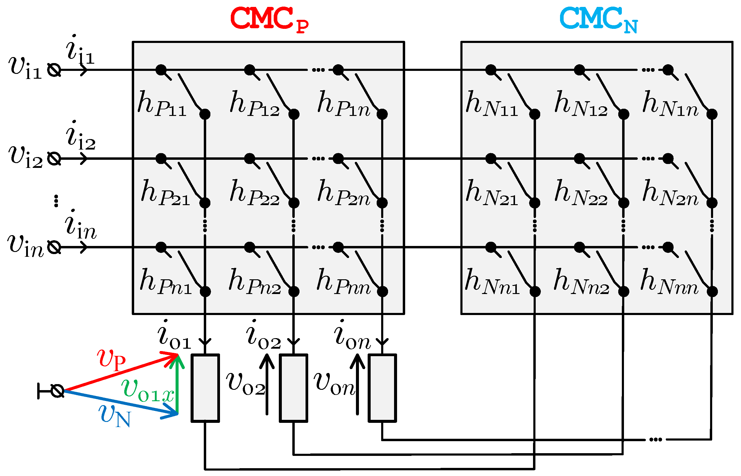
2. The Principle of an Output Voltage Synthesis in DSM-CMC Converter
The DSM-CMC converter consists of two square-type matrix converters, and , connected to load terminals as shown in Figure 1, where the simplified diagram of the circuit is depicted. If the number of load phases is equal to n, the total number of bidirectional power electronic switches is equal to . Both converter are connected with the n-phase AC voltage source , ,…, and . The voltage of the phase of the load
measured at the load terminals, are synthesized by these converters by using the switch group , ,…, .
Figure 1.
Simplified diagram of the square-type double conventional matrix converter.
As can be seen in Figure 2, switches on both sides of one phase of the load make the single commutation cell with two voltage multiplexers, and , respectively.
Figure 2.
The single commutation cell for DSM-CMC 5 × 5.
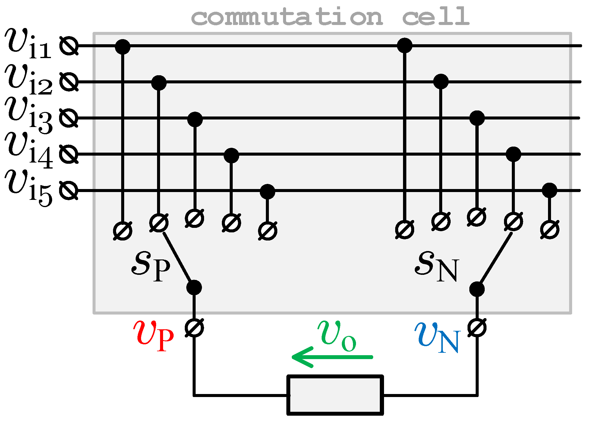
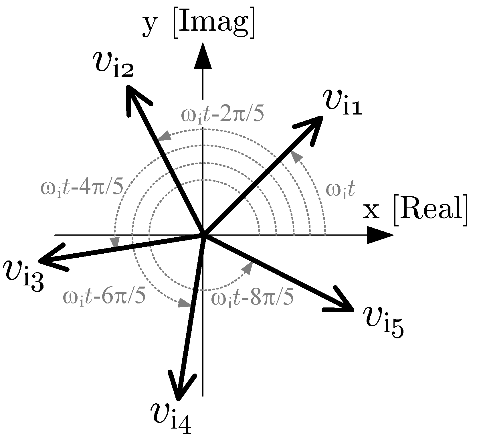
2.1. Case of 5 Phases
The number of multiplexer switches is equal to the number of input voltages, and in this case, takes 5. For a better understanding of the proposal, let the further consideration will be focused on 5 × 5 topology.
According to the proposed concept of the voltage synthesis described in [], all input voltages with pulsation can be represented as a collection of five rotating vectors:
with the real
and the imaginary parts of coordinates
where ,…, are the amplitudes of these voltages. Due to the analytic signal concept based on the Hilbert transform, for the pure sinusoidal input waveforms, the imaginary coordinates are just quadrature components and an input voltage vectors collection can be presented as shown in Figure 3 as the symmetric system.
Figure 3.
The collection of five the rotating input vectors.
These coordinates can be determined using the Hilbert filter or obtained through FFT/DFT based operation [,,]. However, the Hilbert filter and algorithms based on DFT, although are quite accurate, are not the simple solution from code developing point of view. Moreover, error signals in the form of DC offsets, glitches, and momentary voltage sags may occur in measurements. Therefore, the input vector coordinates can be calculated in a different manner. A compromise solution, between accuracy and not complicated solution, maybe the use of the Double Second-Order Generalized Integrator with loop feedback extension functioned as Orthogonal Signal Generator (DSOGI-OSG), which in the OSG part prevents unexpected resonance and variables overflow. DSOGI-OSG structure in continuous time-domain is presented in Figure 4.
Figure 4.
Double Second-Order Generalized Integrator with loop feedback extension functioned as Orthogonal Signal Generator (DSOGI-OSG) structure in continuous time-domain [,,]: —the input sinusoidal signal, —in-phase component of the input signal, —the quadrature component of the input signal, the error signal, k—the gain block, —reference pulsation of the input signal, and ∫ is an integrator block.
The transfer function takes the form of (5) for in-phase output and (6) for orthogonal output, while (7) represents the notch filter equation
where the parameter k is a value less than unity (k is taken the value of here), is the error signal, while is an input voltage nominal pulsation. If processed signal frequency does not have an exact value, another extension of SOGI structure, called Frequency-Locked Loop (FLL), may be applied [,,].
The load voltage produced by the single commutation cell, shown in Figure 2, can be analogous represented by two rotating vectors, and , as is depicted in Figure 5. Only the geometrical distance of real (indicated by subscript ) coordinates of these vectors produce the load voltage. While the imaginary coordinate (indicated by subscript ) can generate the reactive power flow at the converter input. In general, there exists some degree of freedom for selecting the instantaneous value of this component because it does not influence on the load currents. The article is focused on the cases, which locus of each output vector is straight a circle. This means that a rotating output voltage vector moves along a circular trajectory and this movement can be clockwise or counterclockwise. Four variants of the PWM modulation scheme are shown in Figure 5.
Figure 5.
Four variants of output vectors rotation: (a) CCV-CCV, (b) CV-CV, (c) CCV-CV, and (d) CV-CCV.
A vector arrangement in Figure 6a, for the given commutation cell, can be presented as the rotating polygon as illustrated in Figure 6b. The polygon surface is named here as the output voltage synthesis field. All the points, which represent output voltage vectors, have to be located inside the synthesis field. Such a geometric arrangement allows for direct application the Wachspress function for the PWM duty cycles calculation [,]. However, the number of switching within the modulation period should be minimal, and for this reason, Venturini and Wachpress solution is not suitable. Decreasing the number of switching can be realized by applying the Nearest Three Vectors (NTV) modulation technique, which relays on the selection of a proper triangle in the synthesis field. Figure 6c shows two selected triangles for the voltages generated by and converters. Note that both points, representing these voltages, are located in their triangular local synthesis fields. This is the required condition of output voltage synthesizability. The selection of the optimal triangle may consist in finding the appropriate vertex of the synthesis field, which clearly indicates the input vector closest to the output vector. In the case of using NTV technique, this solution is sufficient, because the other two required vectors are adjacent to the selected one. As can be seen, vector is closest to the vertex number 2, while vector is closest to vertex 4. All six required PWM duty cycles can be calculated using the smooth interpolation technique, which is, in the discussed case, nothing more than an appropriate triangle area relation for the NTV modulation []. An area of the triangle can be computed using the second-order matrix determinant. Thus, an application of that solution only needs coordinates of the triangle vertices. As mentioned earlier, these coordinates can be computed using the DSOGI-OSG block shown in Figure 4.
Figure 6.
The principle of operation: (a) vectors arrangement, (b) synthesis field, and (c) selected triangles.
2.2. Case of 12 Phases
In the case of more input voltages, for example, when the number of inputs is equal to 12, the choice of the optimal triangle is not so obvious. Now, let us consider the graphical vector arrangements for topology expressed as regular polygon shown in Figure 7a.
Figure 7.
Synthesis field of the matrix topology (a), the input voltage vectors, and an example reference output voltage (b).
One of 12 presented input vectors is referred here as the base vector. It means that the distance—defined as and shown in Figure 7b—between this vector and the reference vector is the smallest. There are three triangles with a common upper vertex with coordinates : , , and . A vector is the base vector in this case. The given triangle satisfies the modulation conditions when the sum
where
and
of PWM duty cycles , , and takes the smallest value, ideally equal unity. When two or more triangles meet this condition, the triangle with the smallest area should be selected for further consideration. In practice, this operation can be performed by using optimized DSP functions like qsort (sorting in required order), vecmin (finding the minimum value within the set), or standard conditional operators.
When the value of transfer voltage ratio of the 12 × 12 topology, e.g., for or , is in the range
a large number of output phases allows generating the output voltage with lower THD, therefore the cost of passive elements can be decreasing. Corresponding simulation results are presented in the further part of the text. PWM duty cycles calculation for and are explained in two separate subsections. While the two concepts of gating signals generation have been presented in the third subsection.
2.3. PWM Duty Cycles Calculation for and Topology 5 × 5
Referred to the triangle in Figure 6, the reference output voltage is synthesized using 3 switches: , , and . Taking into account previous considerations, the following formulas can be proposed for the calculation of PWM duty cycles,
where det is the determinant of the second-order matrix, and
is the scaling factor, which is equal to the triangle surface. Thus, the average value of the output voltage can be expressed by the following formula.
2.4. PWM Duty Cycles Calculation for and Topology 5 × 5
Referred to the triangle in Figure 6, the reference output voltage is synthesized by 3 switches: , , and . The corresponded duty cycles can be calculate using the following formulas,
where
is the scaling factor, which is equal to the triangle surface. The average value of the output voltage can be expressed by the following formula
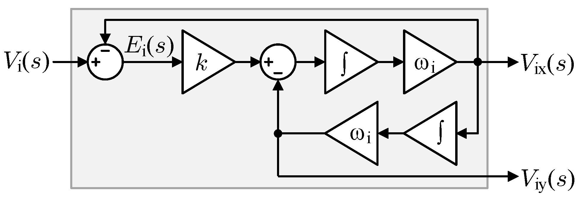
2.5. The Concept of Gating Signals Generation
The gate signals can be controlled according to different strategies. Apap et al. [] compared and presented several PWM signal gating methods. Among them, the cyclic Venturini and Min-Mid-Max (MMM) schemes of modulation are proposed. Two approaches have been applied to the gates signal generation: basic and mentioned MMM scheme.
In the case of the basic solution, the sequences of the switch states always depend on the selected triangle in which the synthesis of the output voltage is realized. Therefore, these sequences can be placed in a lookup table. An overview of the basic sequences is shown in Figure 8, where the value of , which is so-called the golden ratio exists in the pentagon.
Figure 8.
The switch state sequences in the basic solution of the gating signals for both converter cells and .
The MMM method is used to improve the quality of the voltage generated by the converter in terms of THD. The switch states sequences for the and converters are characterized in Figure 9. Note that these sequences correspond to the case illustrated in Figure 6b.
Figure 9.
The MMM type of sequences of the gating signals for both converter cells and for the case depicted in Figure 6c.
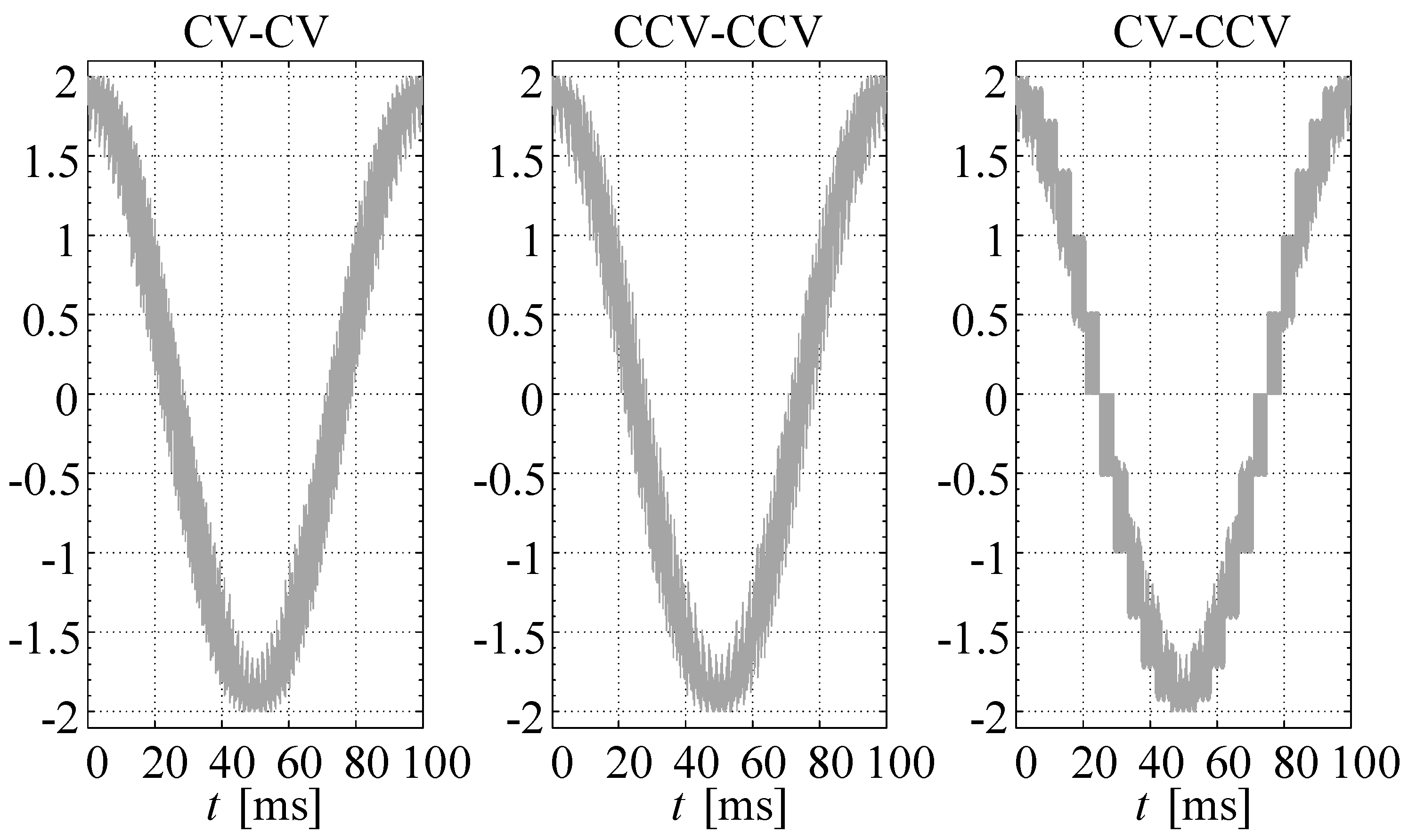
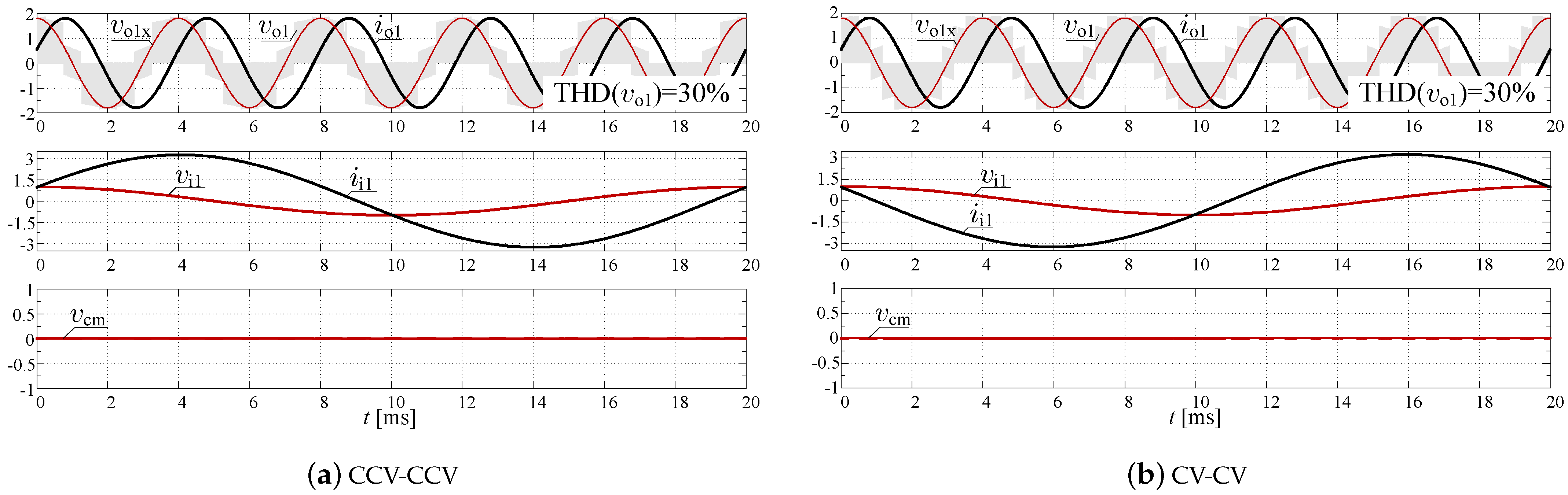
3. The PWM Variant 1—An Output Voltage Synthesis with Zero Value of the Common-Mode Voltage
The common-mode voltage, defined as
can lead to the degradation of rolling bearings in electric machines powered by PWM inverters. As indicated in the introduction an open-end windings stator fed by the double matrix converter allows for the PWM modulation without the common-mode voltage generation. The proposed approach to the load voltage synthesis with conjunction with the basic solution of the gating signals control (shown in Figure 8) give the same desired result. Elimination of the common-mode voltage can be performed by all four PWM modulation schemes: CV-CV, CCV-CCV, CV-CCV, and CCV-CV. The use of the first two cases allows obtaining an input displacement angle, which is dependent on the load parameters like in the Venturini methods [,].
The referenced k-output voltage vectors of the CCV-CCV modulation scheme can be expressed by following equations.
Above equation are proposed for the first commutation cell. Equations for the rest of the rotating vectors pairs can be represented by analogous elaboration. The referenced output voltages in CV-CV scheme can be represented by following equations.
The possibility to change the rotation of the given output vector by changing the sign of the imaginary component allows realizing the PWM modulation, in which the resultant imaginary component of the takes the zero value. If vectors and rotate in opposite directions, as is typical for last two presented schemes of modulation CV-CCV and CCV-CV, the passive input current component is not generated. Simulation results of the PWM variant 1 for DSM-CMC 5 × 5 and four modulation schemes are shown in Figure 10. Simulation parameters are listed in Table A1, which can be found in an appendix.
Figure 10.
Simulation of the PWM variant 1 for DSM-CMC 5 × 5 and four modulation schemes—RL load case.
Analogous simulation tests have been realized for the proposed converter connected to a 12-phase symmetrical power supply. Figure 11 shows the load voltage generated by DSM-CMC12 × 12 for an output frequency equal to 10 Hz, while results obtained for 300 Hz are presented in Figure 12.
Figure 11.
The load voltage for DSM-CMC12 × 12 converter for the three selected modulation schemes: Hz, .
Figure 12.
The load voltage for DSM-CMC12 × 12 converter for the three selected modulation schemes: Hz, .
Simulation parameters for this case are available in Table A2 in Appendix A. The selection of different sets of simulation parameters did not subserve a specific purpose. The simulation tests were carried out with the use of two independent simulation files. However, in the case of the DSM-CMC12 × 12 simulation, a small calculation step was chosen due to the high modulation frequency. It was set to 100 kHz to get a good PWM resolution at 300 Hz of the fundamental frequency.
Properties of this type of matrix converter, compared with counterpart 5 × 5, remains the same. In particular, the common-mode voltage is also eliminated by using the basic type of switches state sequences. The voltages shown in these figures are characterized by a low THD, which is about 12%. Comparing to the 5 × 5 topology, the resulted voltage gain for DSM-CMC is higher and takes optimally the value of .
4. The PWM Variant 2—An Output Voltage Synthesis with Less Harmonic Distortion
The basic solution of the switch states sequence has been applied in the PWM modulation with eliminating the common-mode voltage. If a lower THD of the load voltage waveform is desired, a more advanced gating signal generation mechanism can be proposed, such as MMM scheme shown in Figure 9. With regard to variant 1, this is the only change. However, the MMM method is more complicated because the input voltage vector collection should be arranged in a specific order within the selected triangular synthesis field. Simulation results are presented in Figure 13. A lower THD of the load voltage is obtained but the common-mode voltage is also generated, as marked in the presented drawings.
Figure 13.
Simulation of the PWM variant 2 for DSM-CMC 5 × 5 and four modulation schemes: Hz, .
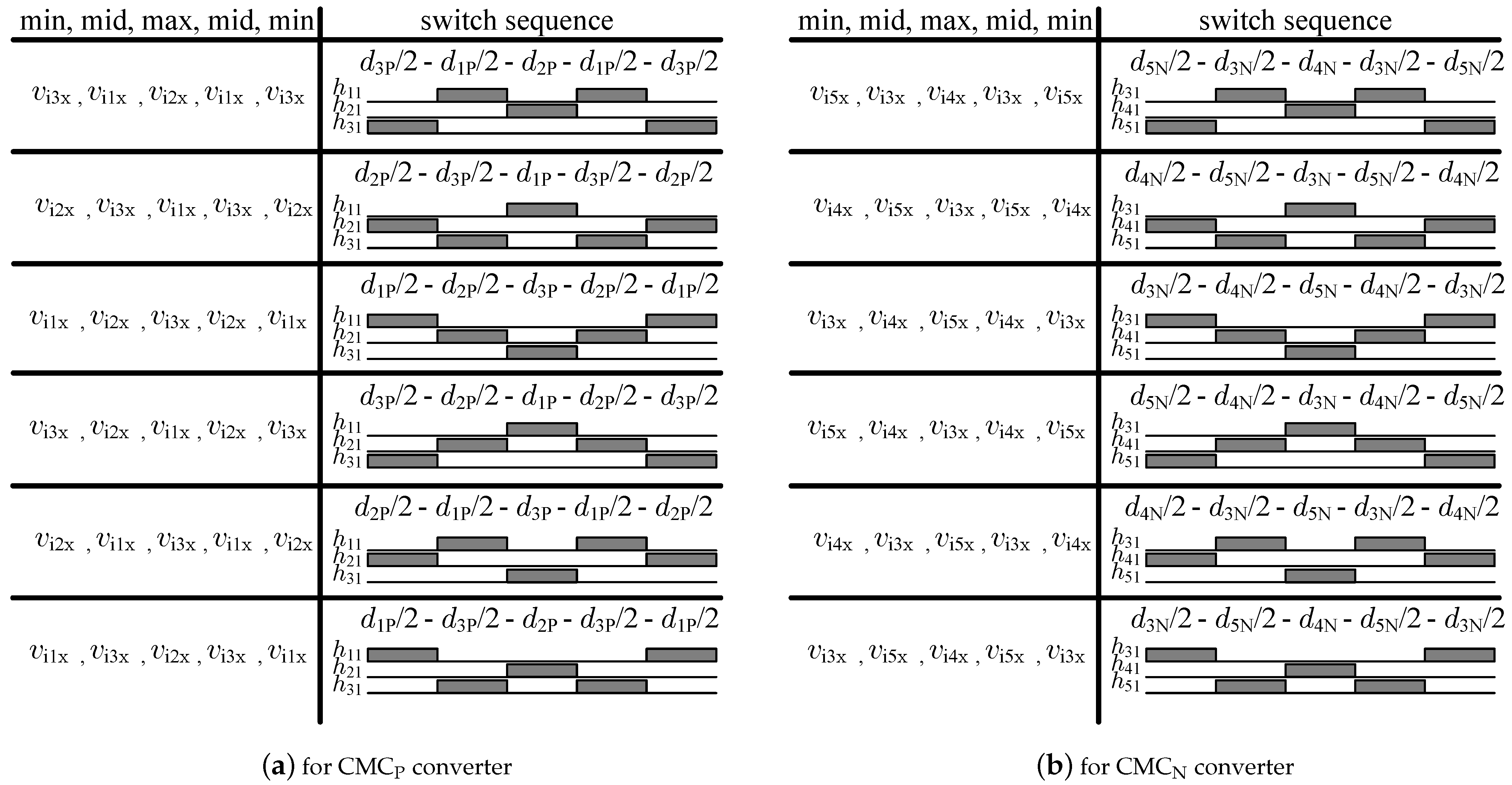
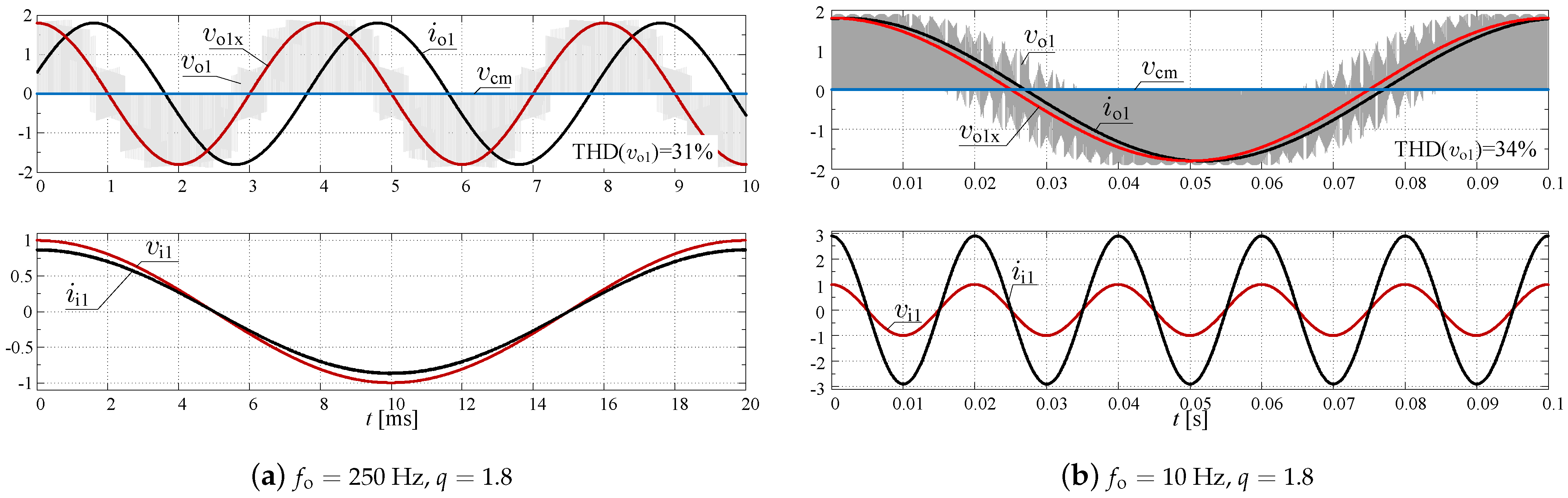
5. The PWM Variant 3—An Output Voltage Synthesis with Maximum Voltage Transfer Ratio and Minimum Number of Switching
A synthesis field for multi-phase and symmetrical AC voltage sources can be represented by a regular polygon as shown in Figure 6b and Figure 7a. A radius of a circle inscribed of this polygon limits an output voltage amplitude in the linear range of modulation. The maximum voltage transfer ratio for and , related to the input voltage amplitude and number of inputs equal to n, can be expressed as follows,
Therefore, the maximum load voltage for DSM-CMC 5 × 5 in is equal to
The value (32) can be increased by modifying the position of the and vectors. In contrast to the methods described in the previous sections, trajectories of these vectors are not a circle. The locus of each vector is not changing smoothly and contains discontinuities. This type of modulation belongs to the discontinuous group of PWM modulations. Both reference vectors and take exactly five positions, in which they lie on one of five input vectors. An algorithm flowchart for DSM-CMC 5 × 5 is presented in Figure 14.
Figure 14.
An algorithm flowchart of the variant 3 PWM modulation: (a) Step 1: generation of synthesis field and reference voltage vectors and . (b) Step 2: calculation of the set of distances between the N point and vertices of the synthesis field. (c) Step 3: calculation of the set of distances between the P point and vertices of the synthesis field. (d) Step 4: shortest distance selection, setting the origin vertex, and the vector’s offset calculation. (e) Step 5: the reference vector shift resulting in the new coordinates of P and N points. (f) Step 6: calculation of four areas of the triangle and PWM duty cycles.
The output voltage synthesis field is generated using the DSOGI blocks at the first step of the proposed algorithm. The reference output voltage vectors coordinates, and , are also calculated at this step. The vectors can rotate clockwise (CV-CV scheme) or counterclockwise (CCV-CCV scheme), as shown in Figure 15.
Figure 15.
An example rotation of the reference output vector.
Based on the analysis of the vector arrangement in Figure 15, it can be written that the maximum length of the voltage vector, in a linear range of modulation, is equal to the following expression.
However, a vector of this length has to be accordingly shifted inside the synthesis field as shown in Figure 14d,e. Therefore, new coordinates of the reference output vector for the given commutation cell can be calculated as follows.
Distances between N-point and all the synthesis field vertices are calculated in Step 2. The same procedure is applied for the point P in Step 3. Next, the shortest calculated distance in a N-collection is compared with the shortest calculated distance in a P-collection . Finally, the less value is selected, which correctly indicates the optimal vertex of the synthesis field. The shift coordinates are calculated in Step 4. As can be seen in Figure 14d, vertex number 4 has been chosen. Thus, the PWM duty cycles, for the case illustrated in Figure 14f can be calculated using the following formulas.
and
Formula (39) refers to the case where the end of the vector coincides with the vector. It means the permanent connection of the input voltage with one side of the load phase during the PWM modulation period. Figure 15 shows a case, which in the one side of the load is permanently connected to an input voltage during PWM modulation. Sequences of the switch states shown in Figure 16 correspond to the case, which in the switch is connected permanently to the input phase 4. The zero load voltage is generated by using the same switch in both and matrix converters. Simulation results for maximal voltage transfer ratio (33) are shown in Figure 17. The common-mode voltage is eliminated. An application of the CV-CV and CCV-CCV scheme of modulation resulting in the non-zero input displacement angle.
Figure 16.
Sequences of the switch states in one commutation cell for the case presented in Figure 14.
Figure 17.
Simulation of the PWM variant 3 for DSM-CMC 5 × 5 and two modulation schemes: Hz, .
Having half the number of switching operations during the PWM modulation period is an advantage of variant 3. In order to obtain the unity power factor at the system input, the sequence types have to be toggled continuously in the order CV-CV, CCV-CCV,…, etc. However, this mode of operation may require to redesign of an input filter. Example simulation results of the PWM variant 3 with toggling mode for DSM-CMC 5 × 5 have been presented in Figure 18.
Figure 18.
Simulation of the PWM variant 3 with toggling mode for DSM-CMC 5 × 5.
6. Summary and Conclusions
This paper presents a new approach to the PWM modulation for the multi-phase matrix converters supplying loads with open-end winding. The proposed approach is an alternative for the methods based on the space-vector modulation. Three variants of PWM modulation were presented. Animations for the first two of them (Figures S1 and S2) are available in Supplementary Materials. The first variant allows for eliminating the common-mode voltage, which is a desired feature from a practical point of view. The second variant based on a specific rearranging switches state sequences can offer quasimultilevel waveforms with low THD. However, a common-mode voltage level can be unaccepted due to influence on the bearings lifetime. Variant 3 of the PWM modulation described in a paper offer over 12% greater voltage transfer gain. Comparison of an input angle value for the proposed variants of PWM modulation is presented in Table 1.
Table 1.
Comparison of an input angle value for the proposed variants of PWM modulation.
The multi-phase matrix converters, with an equal number of input and outputs, belong to the niche solution. Recently, we can observe an increasing interest in multi-phase systems. Furthermore, the complexity of the modulation algorithms grows up. The described proposal is a research result of analytic signal and an application of the smooth interpolation method in PWM duty cycle computing. Some selected features and properties have been compared with the space-vector method. Table 2 presents such a comparison. The PWM duty cycle computation represented by equations, from (12) to (14), is performed using only a second-order determinant of the voltages coordinate matrix without trigonometry usage. Therefore, the proposed method also naturally extends the applicability of the formulas to unbalanced and distorted AC voltage sources. Moreover, all computation can be realized in the FPGA structure using the simple multipliers and adders. The important contribution of the presented article is a presentation of the novel algorithm, which is much easier than algorithms based on the space-vector approach. This property is essential in multi-phase systems because the number of vectors is very high. The proposed solution uses only vectors that represent the Hilbert analytic signal pair calculated for the input and the reference vectors. The number of vectors needed to realize the output voltage synthesis is equal to only the sum of input and output phases.
Table 2.
The comparison of the proposed modulation with the space-vector approach.
Supplementary Materials
The following are available at https://www.mdpi.com/1996-1073/14/2/466/s1, Supplementary data: Matlab script m-file: energies_1056291_Supplementary_Materials.m, Figure S1: A New Approach to the PWM Modulation for the Multiphase Matrix Converters Supplying Loads with Open-End Winding: two rotating the reference vectors, Figure S2: A New Approach to the PWM Modulation for the Multiphase Matrix Converters Supplying Loads with Open-EndWinding: the input and the output waveforms obtained, and the PWM duty cycles.
Author Contributions
The concept, algorithmization, simulation studies, P.S.; simulation results verification and presubmission editing, E.R.-C. and N.S. All authors have read and agreed to the published version of the manuscript.
Funding
This work was supported by the LINTE Laboratory, Gdansk University of Technology.
Conflicts of Interest
All authors declare no conflict of interest.
Appendix A. Simulation Parameters
Table A1.
Simulation parameters for DSM-CMC 5 × 5.
Table A1.
Simulation parameters for DSM-CMC 5 × 5.
| Parameter | Value |
|---|---|
| Number of input voltages | 5 |
| Number of output voltages | 10 |
| Number of an ideal bidirectional switches | 50 |
| Source phase voltage amplitude | |
| Input frequency | |
| Output frequencies | |
| Voltage gain of | |
| Voltage gain of | |
| The load parameters | , |
| An algorithm frequency | |
| Simulation step | |
| Simulation software | PSIM 64-bit Version 11.0.3 |
Table A2.
Simulation parameters for DSM-CMC 12 × 12.
Table A2.
Simulation parameters for DSM-CMC 12 × 12.
| Parameter | Value |
|---|---|
| Number of input voltages | 12 |
| Number of output voltages | 24 |
| Number of an ideal bidirectional switches | 288 |
| Source phase voltage amplitude | |
| Input frequency | |
| Output frequencies | |
| Voltage gain of | |
| Voltage gain of | |
| The load parameters | , |
| An algorithm frequency | |
| Simulation step | |
| Simulation software | PSIM 64–bit Version 11.0.3 |
Simulation research has been performed for symmetric and balanced source and load. Obtained currents and voltages have been presented as values referred to the base voltage and the base current equal to where was a load impedance.
References
- Rodriguez, J.; Rivera, M.; Kolar, J.W.; Wheeler, P.W. A Review of Control and Modulation Methods for Matrix Converters. IEEE Trans. Ind. Electron. 2012, 59, 58–70. [Google Scholar] [CrossRef]
- Friedli, T.; Kolar, J.W. Milestones in Matrix Converter Research. IEEJ J. Ind. Appl. 2012, 1, 2–14. [Google Scholar] [CrossRef]
- Szczepankowski, P.; Wheeler, P.; Bajdecki, T. Application of Analytic Signal and Smooth Interpolation in Pulsewidth Modulation for Conventional Matrix Converters. IEEE Trans. Ind. Electron. 2020, 67, 10011–10023. [Google Scholar] [CrossRef]
- Helle, L.; Larsen, K.B.; Jorgensen, A.H.; Munk-Nielsen, S.; Blaabjerg, F. Evaluation of modulation schemes for three-phase to three-phase matrix converters. IEEE Trans. Ind. Electron. 2004, 51, 158–171. [Google Scholar] [CrossRef]
- Ahmed, S.M.; Abu-Rub, H.; Salam, Z. Common-Mode Voltage Elimination in a Three-to-Five-Phase Dual Matrix Converter Feeding a Five-Phase Open-End Drive Using Space-Vector Modulation Technique. IEEE Trans. Ind. Electron. 2015, 62, 6051–6063. [Google Scholar] [CrossRef]
- Levi, E.; Bojoi, R.; Profumo, F.; Toliyat, H.; Williamson, S. Multi-phase induction motor drives-A technology status review. IET Elect. Power Appl. 2007, 1, 489–516. [Google Scholar] [CrossRef]
- Levi, E. Multi-phase Machines for Variable speed applications. IEEE Trans. Ind. Electron. 2008, 55, 1893–1909. [Google Scholar] [CrossRef]
- Nguyen, T.D.; Lee, H. Development of a Three-to-Five-Phase Indirect Matrix Converter With Carrier-Based PWM Based on Space-Vector Modulation Analysis. IEEE Trans. Ind. Electron. 2016, 63, 13–24. [Google Scholar] [CrossRef]
- Ahmed, S.M.; Salam, Z.; Abu-Rub, H. An Improved Space Vector Modulation for a Three-to-Seven-Phase Matrix Converter With Reduced Number of Switching Vectors. IEEE Trans. Ind. Electron. 2015, 62, 3327–3337. [Google Scholar] [CrossRef]
- Ahmed, S.M.; Iqbal, A.; Abu-Rub, H.; Rodriguez, J.; Rojas, C.; Saleh, M. Simple carrier-based PWM technique for a three-to-nine phase direct AC-AC converter. IEEE Trans. Ind. Electron. 2011, 58, 5014–5023. [Google Scholar] [CrossRef]
- Ahmed, S.M.; Iqbal, A.; Abu-Rub, H. Generalized Duty-Ratio-Based Pulsewidth Modulation Technique for a Three-to-k Phase Matrix Converter. IEEE Trans. Ind. Electron. 2011, 58, 3925–3937. [Google Scholar] [CrossRef]
- El-Khoury, C.N.; Kanaan, H.Y.; Mougharbel, I.; Al-Haddad, K. A review of matrix converters applied to PMSG based wind energy conversion systems. In Proceedings of the IECON 2013—39th Annual Conference of the IEEE Industrial Electronics Society, Vienna, Austria, 10–13 November 2013; pp. 7784–7789. [Google Scholar] [CrossRef]
- Liu, X.; Wang, P.; Loh, P.; Blaabjerg, F. A Three-Phase Dual-Input Matrix Converter for Grid Integration of Two AC Type Energy Resources. IEEE Trans. Ind. Electron. 2013, 60, 20–29. [Google Scholar] [CrossRef]
- Pena, R.; Cardenas, R.; Reyes, E.; Clare, J.; Wheeler, P. Control of a Doubly Fed Induction Generator via an Indirect Matrix Converter With Changing DC Voltage. IEEE Trans. Ind. Electron. 2011, 58, 20–29. [Google Scholar] [CrossRef]
- Garces, A.; Molinas, M. A Study of Efficiency in a Reduced Matrix Converter for Offshore Wind Farms. IEEE Trans. Ind. Electron. 2012, 59, 184–193. [Google Scholar] [CrossRef]
- Abdel-Rahim, O.; Funato, H.; Abu-Rub, H.; Ellabban, O. Multiphase Wind Energy generation with direct matrix converter. In Proceedings of the 2014 IEEE International Conference on Industrial Technology (ICIT), Busan, Korea, 26 February–1 March 2014; pp. 519–523. [Google Scholar] [CrossRef]
- Yaramasu, V.; Wu, B.; Sen, P.C.; Kouro, S.; Narimani, M. High-power wind energy conversion systems: State-of-the-art and emerging technologies. Proc. IEEE 2015, 103, 740–788. [Google Scholar] [CrossRef]
- Zoric, I.; Jones, M.; Levi, E. Arbitrary Power Sharing Among Three-Phase Winding Sets of Multiphase Machines. IEEE Trans. Ind. Electron. 2018, 65, 1128–1139. [Google Scholar] [CrossRef]
- Sienko, T.; Szczepanik, J.; Martis, C. Reactive Power Transfer via Matrix Converter Controlled by the “One Periodical” Algorithm. Energies 2020, 13, 665. [Google Scholar] [CrossRef]
- Rezaoui, M.M. Study of output voltages of a matrix converter feeding an five AC-induction machine using the strategy calculated modulation PMW. In Proceedings of the 2010 Modern Electric Power Systems, Wroclaw, Poland, 20–22 September 2010; pp. 1–4. [Google Scholar]
- Rahman, K.; Iqbal, A.; Al-Hitmi, M.A.; Dordevic, O.; Ahmad, S. Performance Analysis of a Three-to-Five Phase Dual Matrix Converter Based on Space Vector Pulse Width Modulation. IEEE Access 2019, 7, 12307–12318. [Google Scholar] [CrossRef]
- Baranwal, R.; Basu, K.; Mohan, N. Carrier-Based Implementation of SVPWM for Dual Two-Level VSI and Dual Matrix Converter With Zero Common-Mode Voltage. IEEE Trans. Power Electron. 2015, 30, 1471–1487. [Google Scholar] [CrossRef]
- Tewari, S.; Mohan, N. Matrix Converter Based Open-End Winding Drives With Common-Mode Elimination: Topologies, Analysis, and Comparison. IEEE Trans. Power Electron. 2018, 33, 8578–8595. [Google Scholar] [CrossRef]
- Rzasa, J.; Sztajmec, E. Elimination of Common Mode Voltage in the Three-To-Nine-Phase Matrix Converter. Energies 2020, 13, 631. [Google Scholar] [CrossRef]
- Szczepankowski, P.; Bajdecki, T.; Strzelecki, R. Direct Modulation for Conventional Matrix Converters Using Analytical Signals and Barycentric Coordinates. IEEE Access 2020, 8, 22592–22616. [Google Scholar] [CrossRef]
- Malekjamshidi, Z.; Jafari, M.; Zhu, J. Analysis and comparison of direct matrix converters controlled by space vector and Venturini modulations. In Proceedings of the 2015 IEEE 11th International Conference on Power Electronics and Drive Systems, Sydney, Australia, 9–12 June 2015; pp. 635–639. [Google Scholar] [CrossRef]
- Dey, A.K.; Mohapatra, G.; Mohapatra, T.K.; Sharma, R. A Modified Venturini PWM scheme for Matrix converters. In Proceedings of the 2019 IEEE International Conference on Sustainable Energy Technologies and Systems (ICSETS), Bhubaneswar, India, 26 February–1 March 2019; pp. 013–018. [Google Scholar] [CrossRef]
- Ali, M.; Iqbal, A.; Khan, M.R.; Ayyub, M.; Anees, M.A. Generalized Theory and Analysis of Scalar Modulation Techniques for a m × n Matrix Converter. IEEE Trans. Power Electron. 2017, 32, 4864–4877. [Google Scholar] [CrossRef]
- Szczepankowski, P.; Nieznanski, J. Application of Barycentric Coordinates in Space Vector PWM Computations. IEEE Access 2019, 7, 91499–91508. [Google Scholar] [CrossRef]
- Reilly, A.; Frazer, G.; Boashash, B. Analytic signal generation-Tips and traps. IEEE Trans. Signal Process. 1994, 42, 3241–3245. [Google Scholar] [CrossRef]
- Marple, L. Computing the discrete-time “analytic” signal via FFT. IEEE Trans. Signal Process. 1999, 47, 2600–2603. [Google Scholar] [CrossRef]
- Asiminoael, L.; Blaabjerg, F.; Hansen, S. Computing the discrete-time “analytic” signal via FFT. IEEE Ind. Appl. Mag. 2007, 13, 22–33. [Google Scholar] [CrossRef]
- Yan, Q.; Zhao, R.; Yuan, X.; Ma, W.; He, J. A DSOGI-FLL-Based Dead-Time Elimination PWM for Three-Phase Power Converters. IEEE Trans. Power Electron. 2019, 34, 2805–2818. [Google Scholar] [CrossRef]
- Xin, Z.; Zhao, R.; Blaabjerg, F.; Zhang, L.; Loh, P.C. An Improved Flux Observer for Field-Oriented Control of Induction Motors Based on Dual Second-Order Generalized Integrator Frequency-Locked Loop. IEEE J. Emerg. Sel. Top. Power Electron. 2017, 5, 513–525. [Google Scholar] [CrossRef]
- Hoffmann, N.; Lohde, R.; Fischer, M.; Fuchs, F.W.; Asiminoaei, L.; Thøgersen, P.B. A review on fundamental grid-voltage detection methods under highly distorted conditions in distributed power-generation networks. In Proceedings of the 2011 IEEE Energy Conversion Congress and Exposition, Phoenix, AZ, USA, 17–22 September 2011; pp. 3045–3052. [Google Scholar]
- Rodriguez, P.; Luna, A.; Ciobotaru, M.; Teodorescu, R.; Blaabjerg, F. Advanced Grid Synchronization System for Power Converters under Unbalanced and Distorted Operating Conditions. In Proceedings of the IECON 2006—32nd Annual Conference on IEEE Industrial Electronics, Paris, France, 6–10 November 2006; pp. 5173–5178. [Google Scholar]
- Patil, K.R.; Patel, H.H. Modified dual second-order generalised integrator FLL for synchronization of a distributed generator to a weak grid. In Proceedings of the 2016 IEEE 16th International Conference on Environment and Electrical Engineering (EEEIC), Florence, Italy, 7–10 June 2016; pp. 1–5. [Google Scholar]
- He, X.; Geng, H.; Yang, G. A Generalized Design Framework of Notch Filter Based Frequency-Locked Loop for Three-Phase Grid Voltage. IEEE Trans. Ind. Electron. 2018, 65, 7072–7084. [Google Scholar] [CrossRef]
- Apap, M.; Clare, J.; Wheeler, P.; Bradley, K. Analysis and comparison of AC-AC matrix converter control strategies. In Proceedings of the IEEE 34th Annual Conference on Power Electronics Specialist, Acapulco, Mexico, 15–19 June 2003; pp. 1287–1292. [Google Scholar] [CrossRef]
Publisher’s Note: MDPI stays neutral with regard to jurisdictional claims in published maps and institutional affiliations. |
© 2021 by the authors. Licensee MDPI, Basel, Switzerland. This article is an open access article distributed under the terms and conditions of the Creative Commons Attribution (CC BY) license (http://creativecommons.org/licenses/by/4.0/).