Article

A New Filter Concept for High Pulse-Frequency 3-Phase AFE Motor Drives

1
Fraunhofer IZM, Gustav-Meyer-Allee 25, 13355 Berlin, Germany
2
Faculty IV—Electrical Engineering and Computer Science, Technische Universität Berlin, Sekr. TIB 4/2-1, Straße des 17. Juni 135, 10623 Berlin, Germany
*
Author to whom correspondence should be addressed.
Energies 2021, 14(10), 2814; https://doi.org/10.3390/en14102814
Submission received: 22 March 2021 / Revised: 28 April 2021 / Accepted: 6 May 2021 / Published: 13 May 2021
(This article belongs to the Special Issue Electromagnetic Modeling in Power Electronics)

Abstract

:
The size of back-to-back converters with active front end is significantly determined by the size of the passive filter components. This paper presents a new complete EMC filter concept for this type of converter system that is effective on the input and the output. This involves filtering the main common mode interferences from the grid and motor sides with a single CM choke. Since only the difference of the generated common mode voltage-time areas of both converters is absorbed by this component, the size of the required filter can be greatly reduced compared to conventional filter concepts. The concept is validated on a grid feeding inverter that can be connected to the public distribution network with an output power of 63 kW. The size reduction is demonstrated by means of a design example on a system with the same power and electrical requirements. It is elaborated why, applying the new filter concept, the impedance of the DC link potentials to ground and other electrical potentials should be as high as possible and therefore associated parasitic capacitances should be minimized. From this requirement, rules for the design of the power modules of PFC and motor converters for the application of this filter concept are derived.

1. Introduction

1.1. Back-to-Back Converters

Back-to-back converters are widely distributed in the industry. They are utilized in variable speed drives connected to the three-phase public distribution network. In order to comply with the requirements regarding the Total Harmonic Distortion (THD) of the mains current and voltage, in many cases not only the motor inverter but also the rectifier is actively controlled. The basic converter system with this so called Active Front End (AFE) is shown in Figure 1 for the standard 2-level topology addressed in this paper.
One goal of research in the field of back-to-back converters is to increase the power density i.e., the power conversion per physical converter volume. There are various approaches for their size reduction. For example, the utilization of Wide Bandgap (WBG) semiconductors can reduce the size of passive components because it enables the switching frequency to be increased in turn permitting the use of smaller DC link capacitors as well as ripple inductors. Another possibility for volume reduction is the development of new filter topologies.

1.2. Filter Design Considerations

Due to the operation of semiconductors in switched mode, Electromagnetic Compatibility (EMC) disturbances are generated in the converters [1], which must be filtered on the mains side due to EMC requirements, e.g. IEC 61800-3. However, filtering the interferences on the motor side is also reasonable for many applications. On the one hand, differential filtering measures can be applied to prevent high voltage slopes on the motor windings, which can damage the winding insulation due to over-voltages [2]. On the other hand, Common Mode (CM) currents in the motor bearings [3,4] can be reduced [5]. Possibly the motor cable no longer requires a screen because the motor filter reduces the radiated interference to such an extent that the applicable EMC limits can be adhered to. Additionally, motor filters can reduce the occurring losses, especially when long motor cables are used. With each switching operation in the motor inverter the parasitic capacitances of motor and cables must be partially reloaded hard without the application of filters, which leads, among other things, to an increase in switching losses [6,7]. Furthermore, Differential Mode (DM) filtering on the motor side results in lower ripple currents in the cable and in the machine, which leads to the reduction of high-frequency copper losses. Although filters also cause losses, the overall loss balance is usually essentially lower [8].
DM filtering is implemented with a ripple filter stage at each of the half-bridge output nodes. They consist of ripple inductors L r and ripple capacitors C r , as shown in Figure 2. The inductors absorb almost the entire DM voltage-time area, resulting in a relatively high current ripple in the components of the ripple stage, the semiconductors and the DC link capacitors depending on the ripple inductor’s inductance value.
However, both converters also generate a CM voltage that must be reduced for previously described reasons. In [9] it is demonstrated how the CM voltage waveforms in both converters can be made identical by sophisticated voltage pulse generation and thus the CM interference can theoretically be completely eliminated. In fact, in real experiments the CM voltage can be significantly reduced by more than 15 dB , although not completely, due to impediments such as different switching characteristics of the individual semiconductors or dead-time effects (cf. [9]). Another benefit of this measure is that a less saturation-resistant CM choke may be used, since the voltage-time areas, which need to be absorbed, are significantly smaller.
However, for this approach an adjustment of the zero component of the α β 0 system in the space vector modulation [10] is necessary. This represents a disadvantage as the degree of freedom presented by the zero component is used up by the attempt to eliminate the CM voltage and can hence no longer be used for clamping some transistors at specific moments during the mains period i.e., flat-top modulation [11,12]. When flat-top modulation is applied, not only the number of all switching operations can be reduced by one third. Additionally, the amplitude of the fundamental component can be increased by approximately 15% compared to the conventional modulation scheme [11], enabling the DC link voltage in a motor drive system to be reduced by approximately 13%. As a result of both measures, switching losses can be reduced by more than half. Furthermore, the reduction of the DC link voltage unburdens the inductive components, which have to absorb the main part of the voltage-time areas, with regard to the core and High Frequency (HF) copper losses. It can therefore be concluded that with the approach described in [9] flat-top modulation and the DC link voltage reduction would partially not be possible, leaving even more potential for optimization untapped. This is why it makes more sense to select the degree of freedom of the zero-voltage system for flat-top modulation. The disadvantage that components are required which absorb the HF CM voltage-time area must be accepted. In the following sections, it will be worked out how the volume of these components can be minimized.

1.3. Conventional Filter Concepts

Figure 2 shows the drive system using the most frequently used filter topology with respect to the first filter stage (ripple filter) for the PFC [13] and the motor inverter [5]. The filtering of the DM interferences is achieved by the ripple inductors and capacitors. The respective CM current in the PFC and motor inverter closes in two separate current loops via the ripple inductors, the ripple capacitors and the CM capacitor to the DC link as depicted in red in Figure 2. As a result, the ripple inductors absorb not only the differential voltage-time area but also the respective CM voltage-time area of the corresponding inverter. The increased total voltage-time area results in a higher potential for core losses and HF copper losses in the components. Consequently, the ripple inductors need to be much bigger compared to those that only absorb the DM voltage. It is also possible to distribute the CM and DM components between two inductors connected in series [14]. This would require two additional CM chokes in the back-to-back converter.
The low-impedance connection of the capacitor star points to the DC link with the CM capacitors C C M ; M o t complicates the implementation of flat-top modulation on the motor side at low output voltages. Due to the high voltage step at the flat-top transitions, when another half-bridge output node is clamped to a DC link potential, filter oscillations with large current amplitudes occur, which can lead to undesirable effects, for example the saturation of the inductors. The oscillation is formed between the inductance of the parallel-connected ripple inductors and the CM capacitor. To overcome the disadvantages a new CM filter concept with a CM choke in the DC link is proposed in this paper.

1.4. New CM Filter Concept with a CM Choke in the DC Link

The first inductive stage of CM filtering can be provided using only a single CM choke for both inverters. In this case, only the difference in the CM voltage-time areas of the PFC and motor inverter must be absorbed by this component. The ripple inductors of the PFC and the motor inverter are unburdened with respect to the potential for core losses because, in contrast to the common concept from Figure 2, they only absorb the DM voltage-time area. The circuitry requirement of this CM filtering concept is that the two DC link potentials must not have any reference to other electrical potentials. The usually existing low-impedance connection of the ripple capacitors to a DC link potential (see Figure 2) and Y capacitors in the DC link cannot be applied.
The entire filter concept is depicted in Figure 3. As shown, the single circuit for the CM current now contains the PFC semiconductors and inductors, the grid-side ripple capacitors, the CM capacitors on the mains and the motor side, the motor-side ripple capacitors and inductors, the motor inverter semiconductors, and the DC link. The CM choke can be placed anywhere in series with the PFC or motor inductors, but also in the DC link. The arrangement in the DC link has the advantages that only two windings are required, the total current is lower due to the higher DC link voltage compared to the two AC voltages and no DM ripple current occur in the component.
According to the resulting voltage divider from the inductance values of ripple inductors and CM choke, a low CM voltage also drops across the ripple inductors. However, it is negligible due to the inductance value of the CM inductor, which is usually orders of magnitude higher. The high-frequency voltage drop across the ripple capacitors can also be neglected. Nevertheless, they absorb the low-frequency CM voltage which is unavoidable when using flat-top modulation.
The pulse generation of both inverters should be synchronized and both inverters should be operated with the same switching frequency. For instance, a switching period can start with the turn-on of all High Side (HS) switches of PFC and motor inverter. This ensures that the difference between the CM voltages of the PFC and motor inverter remains minimal without adjusting the zero component in the α β 0 system. The degree of freedom for the zero component in the α β 0 system should be utilized for flat-top modulation for the reasons already analyzed. Occurring oscillations due to filter resonances are very low with this concept because they are not excited by the voltage steps at the flat-top transitions but only due to the discontinuity of the pulse patterns.
One disadvantage of this concept is that the CM choke in the DC link introduces an additional leakage inductance between the two DC links. In case of load steps, this can cause undesired oscillations in the DC link voltages. Therefore, this parasitic inductance should be kept very low.
To avoid this problem, it is also feasible that the CM inductor in the DC link is eliminated. In this case, the difference in the CM voltage of the PFC and motor inverter is absorbed by the ripple inductors according to their inductance ratio. Compared to the conventional filter topology, the inductors are also unburdened because they do not absorb the entire CM voltage-time area of the respective converter, but only a part of the difference between the two CM voltages.

1.5. Organization of This Paper

Section 2 contains the applied methods and utilized materials on which the predictions and measurements are based. The prediction methodology for new filter concept introduced in Section 1.4 is experimentally validated in Section 3.1, Section 3.2 and Section 3.3 using the example of a grid-feeding inverter with an output power of 63 kW . Subsequently, design rules regarding parasitic capacitances from the power module and the DC link potential to ground are elaborated in Section 3.4. In Section 3.5 the new filter concept is compared to the conventional topology summarized in Section 1.3, in terms of design, using a typical specification catalog with respect to the size of the CM filter components. Section 4 highlights the conclusions of this paper.

2. Materials and Methods

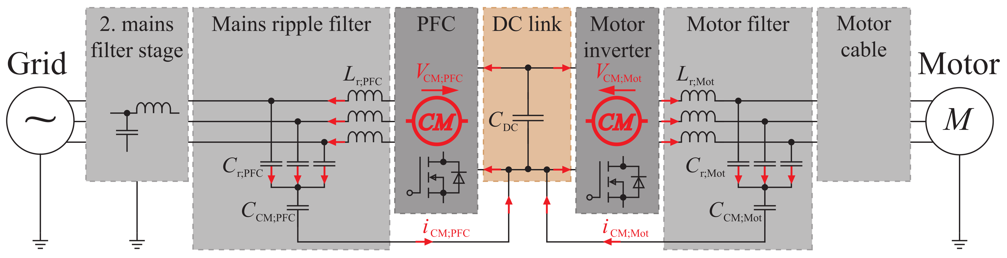
2.1. Experimental Validation Object

Initially, developed models introduced in [15] are compared with measurements. For the validation of the presented filter concept it is not required to operate a complete drive system as shown in 
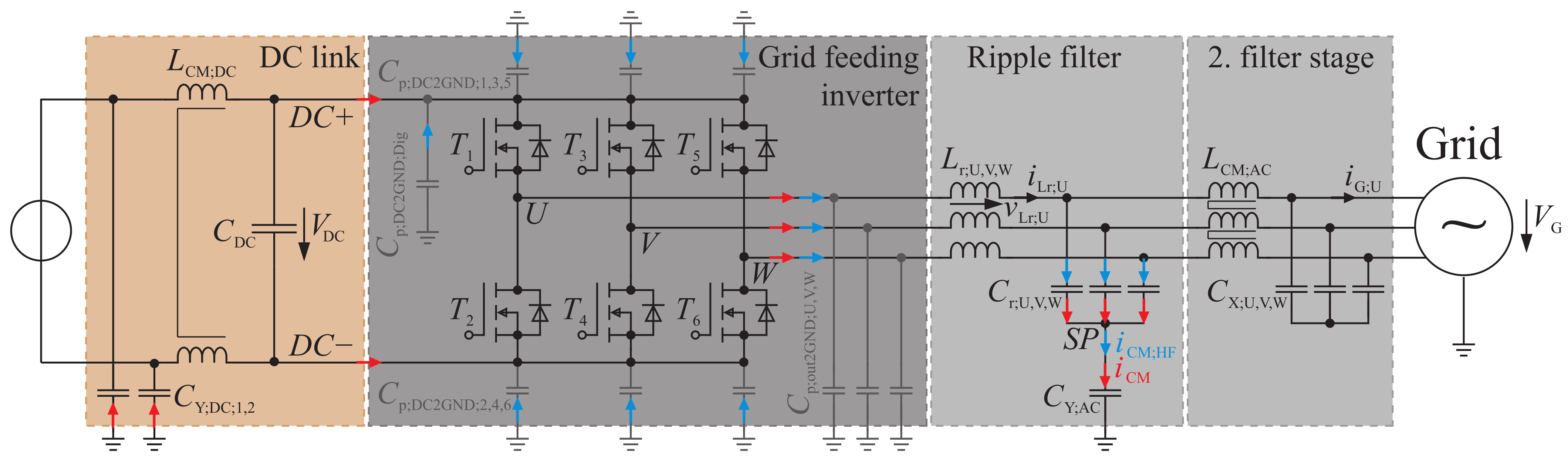
Figure 1. It is sufficient to perform the measurements on the power electronic system presented in 
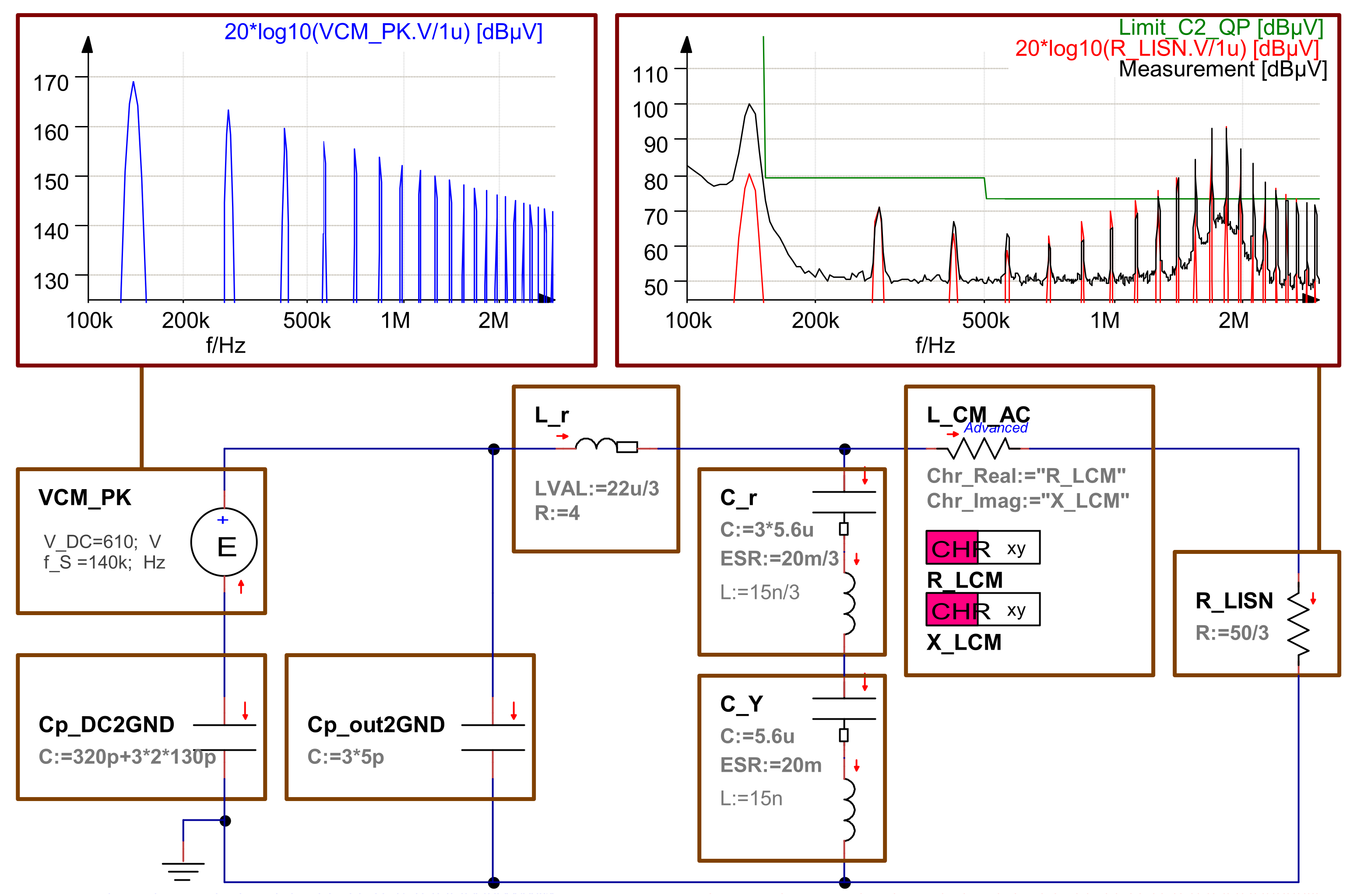
Figure 4. As necessary for the validation, the CM choke in the DC link absorbs almost the entire CM voltage-time area. One difference compared to the complete motor drive is that the load profile of the DC link CM choke regarding the flux linkage differs when the motor inverter is not operated. Consequently, the design results of this choke optimized with respect to losses would differ. Furthermore, without motor and motor cable a CM interference current path is eliminated due to the high capacitive coupling of the motor and cable to ground, which must be considered in the filter design of the complete motor drive system. Despite these differences the validation object is suitable to qualify the approach presented here. The main CM circuit is marked in red in Figure 4 and runs from the semiconductor modules T 1 T 6 through the ripple inductors L r ; U , V , W and capacitors C r ; U , V , W as well as the mains-side Y capacitor C Y ; A C to ground and closes through the Y capacitor on the DC side C Y ; D C and the CM choke L C M ; D C to the DC link potentials. Note that the CM capacitors in the ripple stage and the DC link are Y capacitors connected to ground. Independently of this, a CM current can also be generated without a Y capacitor via the parasitic ground capacitances, which are shown in gray in the figure, since the electrical distribution network has a ground reference.
If the predicted voltage and current waveforms, the voltage-time areas of the ripple inductors and the CM choke in the DC link as well as the interference levels at the considered grid feeding inverter correspond to those measured, the methodology can also be applied to the more complex systems considered previously. Once the validity of the models has been demonstrated, a size comparison can be provided between optimized back-to-back converter system using the novel and the conventional filter topology.
The grid feeding inverter is intended for connection to the public distribution network. Table 1 summarizes its electrical requirements and operating parameters. The DC link capacitor, the ripple inductors and the EMC filter are designed for a switching frequency of f S = 140 kHz . As a result, EMC limits need only be met from the second harmonic at a frequency of 2 f S = 280 kHz , which reduces the size of the filter components.
The prototype inverter used in the measurements is shown in Figure 5. The filters are designed in such a way that their components can be placed at the bottom of the device on a PCB with the same base area as the heat sink. Table 2 contains a list of the applied components with the relevant EMC properties. Note that most of the utilized passive components are not volume optimized.
The impedance of the CM choke on the mains side L C M ; A C cannot be described with frequency-independent parameters because the employed nanocrystalline core material has a strong dependence on frequency with respect to the complex permeability due to increasing eddy currents at higher frequencies. The impedance curve used in the simulations was measured with an impedance analyzer (see below) and is shown in the right diagram of Figure 6.
The frequency dependency of all other specified parameters is not as significant (e.g., L C r , L C Y ) or can be neglected for the modeling (e.g., R C r , R C Y ; A C ), allowing them to be described with frequency-independent values. The parameters were determined by measurements with the impedance analyzer.
The frequency dependence of the ripple inductors’ permeability is neglected, since it drops by only 5 % at the maximum frequency used in the EMI simulations ( 3 MHz ) due to the distributed air gaps in the core material. Furthermore, the winding capacitance of the ripple inductors can also be neglected in the simulations because the first parallel resonance only occurs at a frequency above 10 MHz .
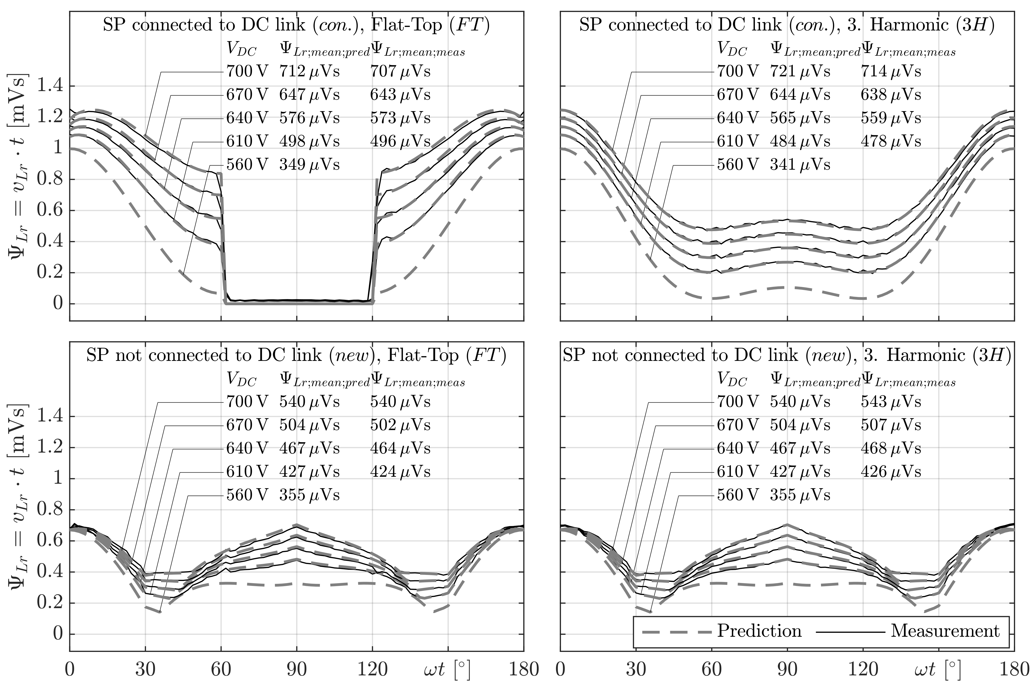
However, it must be considered that the inductance value of the ripple inductors is current-dependent due to the utilization of powder core material KoolMu 60u from Magnetics (https://www.mag-inc.com/Products/Powder-Cores/Kool-Mu-Cores (accessed on 19 July 2019)). On the one hand, their voltage-time area and the CM voltage-time area in the DC link CM choke are affected as a function of the load condition. In the left diagram of Figure 6, the partially empirical equations and parameters for calculating this dependency are provided and the result is compared with the measurement performed with a power choke tester. The current dependent inductance can be predicted with very high accuracy. On the other hand, the current dependent inductance value is reflected in higher interference emissions with increasing load currents as described in the following. the company and must therefore be written with a capital M: “Magnetics”.
The interference measurements are performed at an output power of approximately P o u t = 1.5 kW and a DC link voltage of V D C = 610 V . At the operating point with the highest mains current of approximately i G = 130 A , their inductance value drops from L d i f f = 22 μ H at zero current to 7 μ H . Due to the shifted phase currents of the three inverter stages the emissions does not increase in a proportional manner. Even when one ripple inductor momentarily carries a high current leading to a strongly reduced inductance, the other two inductors will at the same time carry a lower current and thus, relatively seen, maintain a higher inductance. Analyses show that the PK value increases by a maximum of 7 dB and the AV value by 5 dB at full load compared to the low load case.
Special attention is paid to the design of the DC link CM choke, which is designed having the complete motor drive system in mind. Since it must absorb the difference in CM voltage-time areas from both converters, which is relatively high in certain operating conditions, it must be ensured that the choke does not saturate at any operating point and that it is designed for a minimum of losses. The selected core material is a loss-optimized MnZn ferrite for the applied switching frequency with a relatively high saturation flux density of B s a t = 390 mT at a temperature of 100   ° C (N87 from TDK). To keep the leakage inductance as low as possible, two stacks of 5 cores R38.1 × 19.05 × 12.7 are wound with 2 windings of 2 turns each as shown in the right picture of Figure 7. The resulting low leakage inductance of L C M ; D C ; σ = 350 nH per winding including the connections to the two DC links resonates with the DC link capacitors at a frequency of approximately 43 kHz . Due to the damping caused by the losses in the CM choke and especially in the DC link capacitors, which have a relatively high Equivalent Series Resistance (ESR) at this frequency, the oscillation decayed to below 10 % of its initial amplitude after 5 oscillations following a voltage step in one of the two DC link voltages. Since the controller operates with a frequency of 12.5 kHz , no impact on the control is to be expected. However, a load step on the motor side will cause an oscillation with the resonance frequency on the mains side. At this frequency, however, no requirements exist regarding EMC or THD. As the switching frequency is substantially higher than the resonance frequency, no oscillations due to the switching operations of the semiconductors are to be expected. This topic will be subject to further studies in the future.
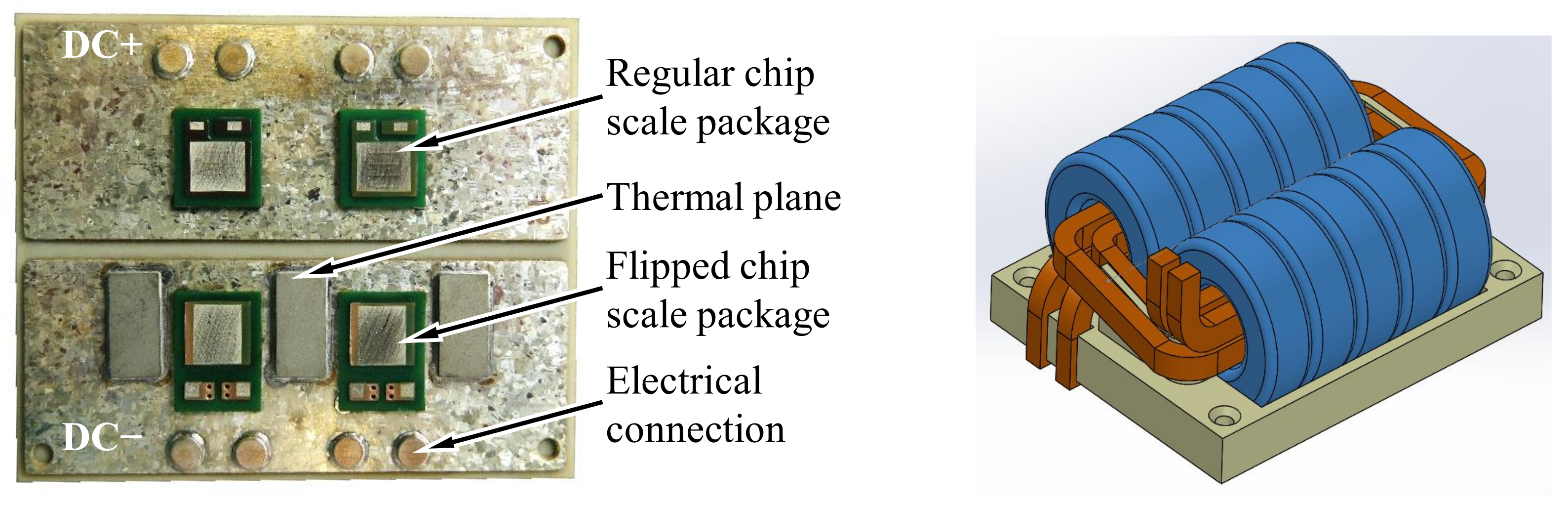
For the validation object, power modules depicted in Figure 7 have been EMC-optimized as described in [16]. The basis for the low-inductive design are Chip-Scale Packages (CSPs) of silicon carbide (SiC) Metal–Oxide–Semiconductor Field-Effect Transistor MOSFET dies, which are also used for the component SCTW100N120G2AG from ST in HiP247 package (https://www.st.com/en/power-transistors/sctw100n120g2ag.html (accessed on 7 October 2020)). The semiconductor dies are each embedded in a small circuit board. One module features four such SiC switches, two in parallel for both High Side (HS) and Low Side (LS).
In the first assembly step, the drain contact of the chip is sintered onto a copper foil. The contacting of the gate and the source is realized with microvias in PCB technology. The LS switches are flipped with respect to their relative position to the Direct Copper Bond (DCB). This is done in order to reduce the parasitic capacitance between the LS drain i.e., the half bridge output potential and the heat sink C p ; o u t 2 G N D ; U , V , W . To avoid imbalances with respect to the occurring parasitic capacitances, the copper areas of the D C + and D C potentials on the top side of the DCB are of equal size. In first approximation the capacitance between top and bottom copper areas can be simply determined using the equation for the capacitance of a plate capacitor and amounts to C p ; D C 2 G N D , 1 6 130 pF (area 33.9 mm × 13.25 mm , the ceramic material silicon nitride S i 3 N 4 is a dielectric with ϵ r = 8.0 and has a thickness of 250 μ m ).
Thermal planes, visible in the picture near the LS switches, are added in order to reduce the thermal resistance between the LS chips and the heat sink: Since the LS switches are flipped, their sinter connection, which have a much better thermal conductivity than the microvias, is not facing the DCB but the inverter PCB. The negative impact this has on the thermal properties is accepted in this case for the benefit of a decreased parasitic capacitance. The additional thermal planes are thermally highly conductive cuboids designed to alleviate thermal problems by transporting heat away from top of the CSPs via copper paths on the inverter PCB back down to the DCB.
The top side of the module is not wire bonded, but soldered onto a PCB. Therefore, the commutation and gate inductances are extraordinarily low allowing for extremely fast switching. Using the loss simulation approach in [17] the switching losses can be predicted neglecting the parasitic module inductances. Hence, it can be concluded that the switching speed is limited exclusively by the semiconductor properties (internal gate resistance, capacitances and transfer characteristic).

2.2. Utilized Measurement Devices

The inverter system described above was operated and monitored during operation using the following instruments:
  • Oscilloscope with 5 GHz bandwidth Tektronix MSO58;
  • 2 DC voltage sources Delta Elektronika SM1500-CP-30;
  • High-voltage, isolated, differential voltage probes PMK BumbleBee;
  • Current clamps Tektronix TCP0150;
  • Line impedance stabilization network 3 Rohde & Schwarz ESH3-Z6.
An Agilent 4294A impedance analyzer was used for impedance measurements. Furthermore a DPG10 power choke tester was applied for inductance measurements in dependence on the current. The evaluation of the interference emissions was performed with PK detector measurements using an EMC test receiver Rohde & Schwarz ESU-8.

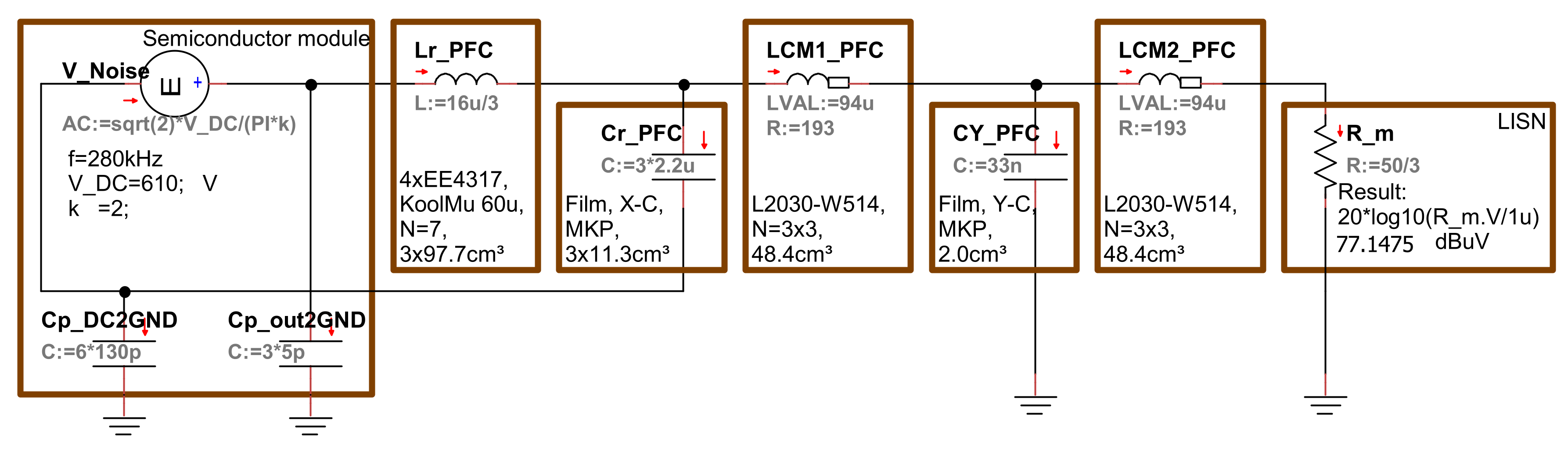
2.3. Filter Design Assumptions

After providing experimental evidence of the accuracy of the existing prediction methodology, conventional and novel filter topologies are compared using computational methods. As already mentioned, the analytical calculation tool presented in [15] is used for the calculations. It enables a large number of design possibilities to be calculated in a short time.
The models predict the operating behavior of back-to-back converter systems with AFE according to Figure 2 and Figure 3 respectively, assumed to have a rated power of 63 kW and being connected to the public distribution network. Mains phase Root Mean Square (RMS) voltage is V G = 230 V , mains frequency is f G = 50 Hz . The maximum DC link voltage is set to V D C = 610 V , a switching frequency of f S = 140 kHz and flat-top modulation is considered.
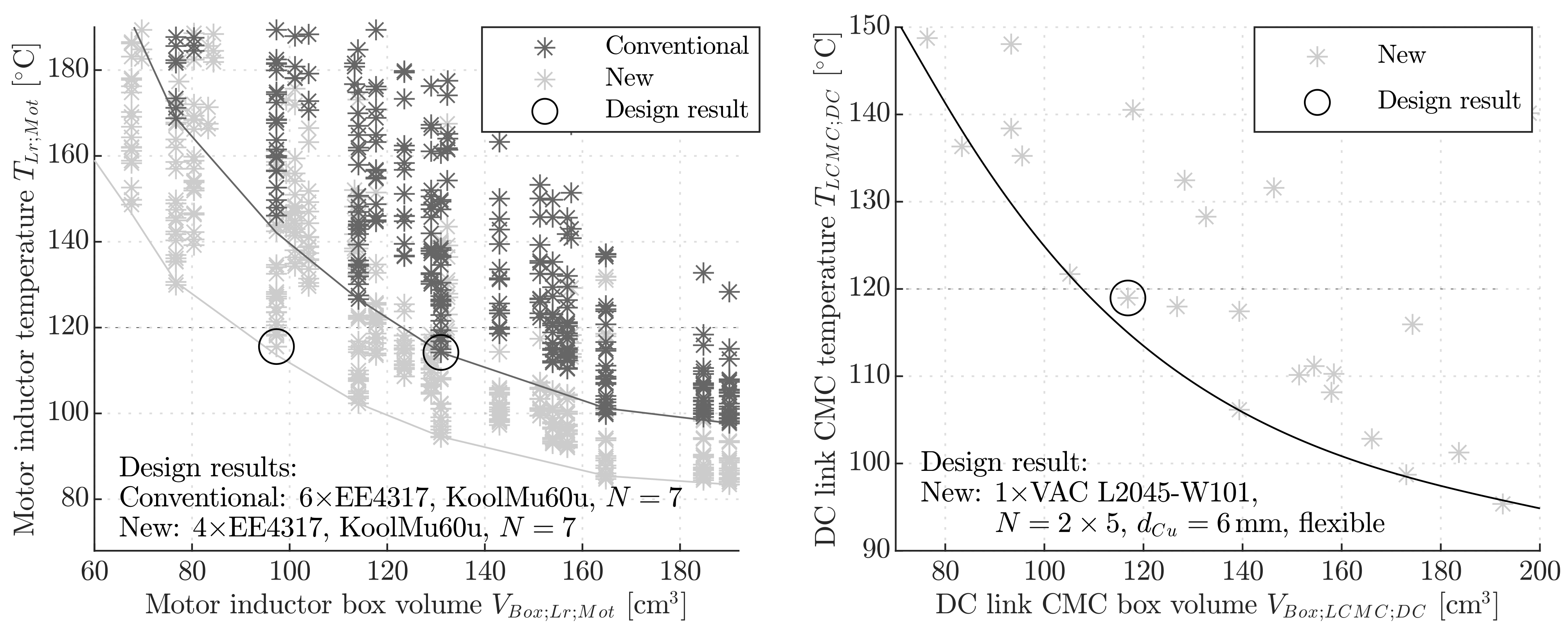
For thermal modeling it is assumed, that the ambient temperature is T a = 60   ° C maximum and that the winding temperature of the inductors and CM chokes must not exceed T L = 120   ° C . Furthermore, it is assumed that the entire surface of the inductors can dissipate a power of k = 50 W / ( m 2 K ) to the environment via forced air cooling.
The ripple inductors on the PFC and motor side as well as the DC link CM choke can be designed independently of all other passive components because they are configured according to the lowest losses and not according to EMC attenuation characteristics. Since PFC ripple inductors always absorb the difference between mains and DC link voltage, losses are maximum at full load. The output voltage on the motor side can be varied over a wide range, resulting in the voltage-time area of the associated ripple inductors being much higher than that of the PFC inductors. It makes sense to analyze and compare designs at the operating point of maximum losses. With the use of the analytical calculation tool mentioned above a motor voltage of 145 V and a motor current of 91.3 A is therefore chosen.
With respect to possible core materials, different powder materials are compared, namely the powder material KoolMu from Magnetics with relative permeability of 40, 60 and 90 and the amorphous iron based alloy material 2605SA1 Metglas (https://metglas.com/magnetic-materials/ (accessed on 20 February 2021)). Their parameters were taken from their respective datasheets and used to calculate the core losses applying the improved generalized Steinmetz equation [18,19,20]. The Steinmetz parameters are listed in Table 3. The factor for calculation with a sinusoidal excitation k p is converted for use in the generalized Steinmetz equation as described in [20]. The dependence of the core losses on the premagnetization [21] is neglected for simplicity. The core shapes considered for the design are limited to the standard cores available from the manufacturers. E cores are considered for the KoolMu cores and AMCC cores for the Metglas cores.
Since the permeability of the core materials strongly changes with the magnetic field strength, the dependence of the differential inductance of the inductors on the current is taken into account by the calculation tool (cf. left hand diagram of Figure 6). To simplify the calculation of the current ripple, the average differential inductance during a switching period corresponding to the instantaneous low-frequency load current is used. The error that occurs is negligible.
A single-layer rectangular winding with wires bent over the thinner edge is used as winding, which ensures a high copper fill factor and low HF copper losses in the components. Such rectangular wires are available in a large geometric variety. Therefore, the width and height of the winding wire are automatically calculated by the calculation tool, taking into account the necessary insulation distances and manufacturability. Those are assumed to be 1 mm between copper and core where the wire is surrounded by core material, 5 mm where the winding runs outside the core and 300 μ m from one turn to the next. The frequency-dependent resistance of the winding is calculated with a 2D FEM simulation at an assumed winding temperature of T L = 120   ° C . The results are used to determine the Low Frequency (LF) and HF copper losses. In this process, just the resistance in the winding part enclosed by core material is calculated. Since the HF copper losses are only a small part of the inductor losses, it is assumed that the current density distribution is identical in the winding part outside the core. To account for the copper losses in the winding part that is not enclosed by the core material, the resistance calculated with the FEM is multiplied by the winding factor. This is calculated analytically previously and specifies the ratio of the actual length of the winding wire to the length considered in the simulation.
For the design of the CM choke in the DC link it is important to note that there is no operating point at which all designed chokes have the maximum losses. In the case of motor start-up, core losses occur almost exclusively, because the current in the DC link is very low due to the low output voltage. At this operating point, the core losses are at a maximum. A CM choke optimized for this operating point would have a large number of turns and a winding wire with a low copper cross-section. In contrast to this, however, at maximum output power the copper losses are maximum, but the potential for core losses is not as pronounced. Therefore, several operating points must be considered for the design of the CM choke in the DC link. Table 4 shows the operating points used for the choke design.
Standard ring cores made of nanocrystalline core material from Vacuumschmelze (https://vacuumschmelze.com/products/Inductive-Components-and-Cores/Amorphous-and-Nanocrystalline-Cores (accessed on 17 February 2021)) are used in the design. Since the geometric dimensions are not very fine-grained, not as many variants as for the ripple inductor design can be calculated. In the loss modeling, the HF copper losses are neglected because the switching-frequency current is very low due to the high inductance value of the CM choke. The core losses are calculated using the generalized Steinmetz equation with the parameters specified in Table 3. The low-frequency copper losses result from the determined DC resistance of the flexible copper winding wire at a temperature of T L = 120   ° C and the DC link current. The latter and the voltage-time area that the CM choke must absorb are determined using the calculation tool presented in [15]. Furthermore, it must be ensured that the core material is not saturated at any operating point. It is also taken into account that the CM voltages are load dependent due to the current dependence of the differential inductance of the ripple inductors (cf. Section 3.1 and Section 3.2).
For the EMC filter design the following assumptions are made. Since the switching frequency is selected with f S = 140 kHz and EMC limits values exist from a frequency of 150 kHz , the filters are designed for the interference levels at the second harmonic of the switching frequency. The interference excitation is considered to be a square wave voltage with a voltage step corresponding to the DC link voltage V D C and the highest possible interference voltage value for the harmonic under consideration. The Fourier transformed value for these assumptions results in the PK interference voltage in the frequency domain V N o i s e :
V N o i s e = 2 V D C π k
where k is the number of the harmonic which is 2 for the design frequency of 280 kHz .
In order to comply with the EMC regulation limit values on the mains side according to IEC 61800-3 Class C2, further filter components are required in addition to the ripple filter. For the frequency of 280 kHz the PK limit value is 79 dB μ V . To enable the cable shield to be eliminated on the motor side, the PK interference voltage must not exceed 80 dB μ V in the frequency range 150– 500 kHz in accordance with the CISPR 14 standard. For this purpose, the interference voltage on the motor side is measured at an input impedance of the measuring device of 1500 Ω .
The EMC filters are designed according to the PK value. Although the PK and AV values differ by only about 5 dB for a LF sinusoidal excitation, the limits according to IEC 61800-3 Class C2 differ by 13 dB . However, the AV value of the interference can be reduced to the desired difference to the PK value using frequency dithering according to [22,23]. Since the measurement bandwidth of 9 kHz is much smaller than the average switching frequency, the AV value can be reduced widely by more than 10 dB . The PK value cannot be influenced by frequency dithering.
For the size comparison, only the CM filter volume is considered. It is assumed that EMC optimized power modules are utilized. For the conventional topology, this means a minimum ground capacitance of the half-bridge output nodes C p ; o u t 2 G N D according to the design rules in [16]. In contrast, in the case of using the CM filter concept with the CM choke in the DC link, the parasitic capacitances of the DC link potentials C p ; D C 2 G N D must be minimized. In the simulations, it is assumed that the module layout is optimized to reduce these capacitances to 5 pF per phase. For the other parasitic ground capacitances of the semiconductor module, a total capacitance of 6 × 130 pF is considered.
As described in [14] the overall capacitance value of all Y capacitors on the mains side must be limited due to safety requirements to a total value of 35 nF . Behind the ripple inductors on the mains and motor side respectively, X capacitors with non-restricted capacitance value can be used for CM filtering because they do not have to be connected to the ground potential. The CM capacitors C C M ; P F C and C C M ; M o t in Figure 2 and Figure 3 can be omitted. The three capacitors C r ; P F C and C r ; M o t , respectively, are used on each side, each connected to one of the three phases. Thus they have an effect for filtering the CM and DM interferences. Their connection between the mains and motor sides when using the new filter topology or to the DC link potential when using the conventional filter topology must be very low inductive. Assuming three X capacitors with a capacitance value of 2.2 μ F each and a parasitic inductance of 20 nH , the impedance of the CM current path is determined exclusively by the inductance from the fourth harmonic on.
The required size of the DM filter is not influenced by the components of the CM filter in this case. Although leakage inductances of the CM chokes have an influence on the DM attenuation, but in this case they have such a minor influence with values in the range of only 100– 200 nH that they can be neglected. To minimize the DM filter, additional DM filter chokes are needed to reduce the size of the X capacitors.
The design is done with simple circuit simulation with the simulation program Portunus (https://www.adapted-solutions.com/en/home-englisch/ (accessed on 28 February 2021)). Due to the limited number of available cores made of nanocrystalline core material from Vacuumschmelze, no calculation with the optimization tool for the CM filter is required.
As almost the entire voltage-time area is absorbed by the CM choke in the DC link or by the ripple inductors, and outside the ripple stages the ripple currents are negligible, only the LF copper losses are considered for further required CM chokes. The inductance and resistance values of the CM chokes are calculated according to the cross-section and path length of the utilized core, the complex permeability of the nanocrystalline core material at the design frequency of 280 kHz , as well as the number of turns.

3. Results and Discussion

3.1. Comparison of Predicted and Measured Current and Voltage Waveforms

Since the CM voltage is absorbed by the DC link, the current and voltage waveforms differ from those using the conventional filter topology. To increase the understanding of the system, current and voltage waveforms in the ripple stage are initially analyzed. The left diagram of Figure 8 shows the comparison of measurement (gray) and prediction (red) of the ripple inductor and mains current at an output power of P o u t = 25 kW and operation with flat-top modulation over one mains period in phase U. For better comparability, the predicted inductor current waveform is shown with the envelope of minimum and maximum current i L r ; m i n , i L r ; m a x .
In the measured waveforms of the inductor and mains currents, small inhomogeneities can be seen at multiples of Δ ω t = 60 ° . The cause can be explained by the fact that at these points in time the switch, which is permanently turned on, is changed (at ω t 60 ° from T 6 to T 1 ). However, the requirements regarding the THD are still met.
Slight differences can be recognized between the positive and negative inductor current half-waves with regard to the minimum and maximum values. They are caused by the fact that always all top transistors are turned on simultaneously at the beginning of a switching period.
The diagram on the right in Figure 8 shows the curves of inductor current and voltage over a switching period at the arbitrarily chosen mains angle of ω t = 20.8 ° . The representation of the control signals shows that the half bridge output of phase W is currently clamped to the DC minus potential ( T 6 is permanently turned on). The control signal value of 0 indicates that the bottom semiconductor is activated. If the value of 1 is assigned to the control signal, the respective top switch is turned on. Occurring dead times ( t d e a d = 125 ns ) could be assigned to one of both possible states depending on the inductor current direction, but are neglected by the calculation tool, resulting in small time deviations from the measured curves of the inductor voltage (here at ω t = 20.83 ° ). As can be seen, the developed analytical calculation tool [15] enables a precise prediction of all current and voltage characteristics.
It can be seen that the voltage across the ripple inductor changes not only when the switching state of the associated half-bridge changes, but also when that of the other two half-bridges changes. The reason for this is the absence of a low-impedance connection of the filter to the DC link potentials. As a result, the CM voltage drops across the DC link potentials. Assuming current-independent inductance values of the ripple inductors, the CM voltage changes by one third of the DC link voltage for each change in switching state. However, since the inductance value of the ripple inductors is current-dependent and different mains currents flow in the three inductors due to the phase shift of 120 , the CM voltage steps and thus also the inductor voltage steps differ from each other when the switching state of the three half-bridges changes. In the example shown at ω t = 20.8 ° , the current in phase U is the smallest compared to the other phases, the inductance value of the ripple inductor is the highest and consequently the CM voltage step when switching phase U is the lowest. At a DC link voltage of V D C = 610 V , the CM voltage step at switching in phase U at this operating point is only 176 V instead of 203 V and the inductor voltage changes by 434 V instead of 407 V . Consequently, for the accurate prediction of the voltage-time areas in the ripple inductors and the DC link CM choke, the current dependence of the inductance value of the ripple inductors L r = f ( I ) must be taken into account.

3.2. Voltage Time Area of the Ripple Inductor and CM Choke

For the design of inductive components, the determination of the losses is of central importance. Only if the voltage-time areas in the inductors are correctly determined, the core losses can be calculated with high accuracy. For the validation of the design results regarding the core losses from Section 3.5, the predicted voltage-time areas are compared with those measured.
Figure 9 presents the voltage-time areas absorbed by the ripple inductor Ψ L r = v L r · t for different configurations as a function of the mains angle ω t for 5 different DC link voltages and an output power of P o u t = 11 kW in reactive power neutral operation c o s φ = 1 at a switching frequency of f S = 140 kHz and a mains voltage of V G = 228 V in each case. The flux linkage Ψ L r corresponds to the area below the inductor voltage-time curve when the inductor voltage is positive during a switching period 1 / f S . Illustratively, the voltage-time area for the switching period shown in the right hand diagram of Figure 8 can be calculated with the time interval when the top semiconductor of phase U is activated as Ψ L r = 110 V × 4.84 μ s = 0.532 mVs . This value can also be found in the bottom left diagram at a mains angle of ω t = 20.8 ° and a DC link voltage of V D C = 610 V . The magnitude of the negative voltage-time area is almost the same. The low-frequency component and the occurring losses can be neglected.
Since the waveforms are identical from ω t = 180 ° to 360 , the plots are limited to a half mains period. The capacitor star point S P is either connected to the DC minus potential ( c o n . ) which is related to the conventional filter topology or not connected ( n e w ) what corresponds to the operation with the new filter topology. In addition, the inverter is optionally operated with the injection of a 3rd harmonic ( 3 H ) and with flat-top modulation ( F T ).
The flux linkages calculated with the analytical model are shown by the gray dashed lines. It can be seen that the flux linkages can be predicted with high accuracy in all operating conditions. More substantial deviations between measurement and prediction occur in operation with flat-top modulation shortly after another half-bridge transistor is clamped. The filter-frequency oscillations excited during this process slightly increase the voltage-time area in the inductor for a short time. Additionally, there are small dead-time related calculation inaccuracies.
The voltage-time area waveforms for operation with an injected 3rd harmonic and flat-top modulation are identical when the filter is not connected to the DC link ( n e w ). The reason for this is that the adjusted voltage vectors in the space vector diagram are the same for these two operating conditions and the voltage-time area generated by the zero component of the α β 0 system (CM) does not occur in the ripple inductor but in the DC link CM choke in this setup configuration. In contrast, in the case of a low-impedance connection between the ripple capacitor star point and the DC link ( c o n . ), the ripple inductor must absorb the switching-frequency CM voltage. Therefore, its voltage-time area is considerably higher which leads to higher core loss potential. The low frequency CM voltage drops across the ripple capacitors C r ; U , C r ; V , C r ; W . Since the CM voltage differs in operation with imprinted 3rd harmonic and flat-top modulation, the voltage-time-area waveforms are also different.
The disproportionate increase of the voltage-time area with the DC link voltage Ψ L r ; m e a n = f ( V D C ) is caused by the disproportionate increase of the difference between DC voltage and mains voltage. However, it is noticeable that the increase in the mean value of the voltage-time area in the ripple inductors rises with an exponent of approximately 3.2 when the conventional filter topology is used ( c o n . ), whereas this exponent is only approximately 1.9 when the filter topology with DC link CM choke is applied ( n e w ). It can be concluded from this that the ripple inductors are unburdened particularly regarding core loss potential at high DC link voltages when the new filter topology is used.
As mentioned earlier, when using ripple inductors with current-dependent inductance applying the new filter topology, the CM voltage changes as a function of the load condition and thus also influences the voltage-time area that the DC link CM choke absorbs. Figure 10 shows the voltage-time areas over half a mains period for three different load conditions. It can be predicted with high accuracy.
As the load increases, the voltage-time area becomes lower, reducing the potential for core losses. This has a positive influence on the design of the choke because the copper losses increase with the load and thus the overall loss profile is more balanced as a function of the load condition.

3.3. EMC Measurements

The CM emissions of the system with the new filter concept described in Section 2.1 are modeled and measured. In Figure 11 the circuit model is depicted for the prediction of CM emissions. As can be seen in the diagrams, the evaluation of the interference levels measured by the test receiver with the measurement bandwidth of 9 kHz is already included in the voltage source model of the interference excitation V C M _ P K . For this purpose, the equation
Δ V = e l n 2 · Δ f f B W 2 2
given in [24] is implemented in the circuit simulation. For the CM interferences, the ripple inductors, the resistors of the Line Impedance Stabilization Network (LISN), the X capacitors and the parasitic capacitances of the DC link potentials to ground are each connected in parallel. This is taken into account in the simulation by a factor of three or one third (see Figure 11). In the right-hand diagram the red curve depicts the predicted emissions, while the black curve shows the result of the interference measurement, in the frequency range between 100 kHz and 3 MHz . It can be recognized that only the switching-frequency harmonic at 140 kHz exceeds the prediction for CM emissions. According to the inductance and capacitance values of the used components listed in Table 2, these interference levels can be clearly attributed to DM interferences, which will not be analyzed further here.
The interference emissions can be reproduced from the second harmonic onwards with the presented circuit simulation. This only requires consideration of the CM path shown in blue in Figure 4. It can be concluded, that the ground capacitances of the DC link potentials C p ; D C 2 G N D play a key role for the modeling these results. These parasitic capacitances are so high that, above a frequency of about 400 kHz , their impedance is lower than that of the CM current path via the DC side Y capacitor and the DC link CM choke, which is marked in red in Figure 4.
The limit exceedance by about 20 dB at a frequency of approximately 1.7 MHz arises due to the resonance of the CM inductance of the ripple inductors L r / 3 with the parasitic capacitance of the DC link potentials to ground C p ; D C 2 G N D . Due to the strong capacitive coupling of the DC link potentials to digital ground caused by the PCB design and the DC link voltage measurement, a portion of C p ; D C 2 G N D ; D i g = 320 pF is added to the parasitic ground capacitance caused by the semiconductor modules C p ; D C 2 G N D ; 1 6 .
This oscillation can also be seen in the inductor voltage in the right-hand diagrams of Figure 8. However, in this measurement the semiconductor modules were removed from the heat sink. As a result, the resonant frequency increases to approximately 3.3 MHz corresponding to the lower ground capacitance of the DC link potentials ( C p ; D C 2 G N D = C p ; D C 2 G N D ; D i g ) and the interference emissions are reduced by approximately 10 dB . The related EMC interference measurement results are shown in the left diagram of Figure 12.
In contrast to the design rules worked out in [16], it can be concluded from these results that when using the introduced filter concept the ground capacitance of the DC link potentials should ideally be minimized.
The right diagram of Figure 12 shows the interference emissions when wired capacitors with a capacitance value of C p ; o u t 2 G N D ; 1 3 = 480 pF each are additionally connected between the half-bridge output nodes and ground. It can be seen that with this measure the resonance at 3.3 MHz which exceeds the limit value can be suppressed. Due to their low impedance, these capacitors return the CM interference current back to the source and can thus be regarded as the first CM filter stage. Since the capacitors and especially their connections with wires have a very high parasitic inductance of about 90 nH , there is a significant resonance at approximately 24 MHz which exceeds regulation limits. However, the interference emissions at the frequencies in the MHz range can be expected to be below the limit values if the ground capacitances of the half-bridge output nodes are not generated by wired capacitors, but by parasitic module capacitances.

3.4. Derivation of Design Rules for an EMC Optimized Power Module

From these results, design rules for the semiconductor modules when using the new filter topology can be derived. In contrast to the design rules from [16], when using the new filter concept presented here, not the ground capacitances of the half-bridge output potentials C p ; o u t 2 G N D but those of the DC link potentials C p ; D C 2 G N D must be minimized in order to optimize EMC. Therefore, not the bottom but the top semiconductors in the power module have to be flipped. In addition, parasitic capacitive couplings of the DC link potentials to all other electrical potentials, such as digital supply and ground potentials as well as measurement lines, need to be minimized. Furthermore, the parasitic capacitances of the half-bridge output nodes should be high and must be the same in all three half-bridges to avoid the generation of CM currents. With each switching operation, the associated ground capacitance of the half-bridge output node is reloaded by two thirds of the DC link voltage. The amount of charge required for this is exactly the same as the amount of charge required for reloading the other two capacitances that change their voltage by one third of the DC link voltage, assuming all half-bridge outputs have the same ground capacitance. Due to the fact that the directions of the currents are distributed in such a way that the current flowing out of the half-bridge outputs is exactly as high as the current flowing in, the change of the switching states of the half-bridges does not cause a CM interference.

3.5. Design Comparison

After verifying the models, the back-to-back converters when using the conventional and the new filter topology can now be optimized according to to assumptions in Section 2.3 and compared with each other in terms of the required volumes.
Figure 13 illustrates the design results for the ripple inductors of the PFC. The left diagram shows the losses and the right diagram the calculated temperature as a function of the inductor volume. From the large number of more than 600 calculated inductor variants, a Pareto front is obtained for each of the assumptions made, which is shown with the solid lines. Based on this, the respective loss and volume optimized inductors can be determined (new filter concept: 3xEE4317, KoolMu 60u, N = 7 , A C u = 6.0 mm × 2.5 mm , L n o m = 22 μ H , V = 80.4 cm 3 , P L r = 32.9 W , conventional filter concept: 4xEE4317, KoolMu 60u, N = 7 , A C u = 6.0 mm × 2.5 mm , L n o m = 29 μ H , V = 97.7 cm 3 , P L r ; M o t o r = 40.8 W ).
For the motor inductor, only the dependence of the volume on the temperature is shown in the left diagram of Figure 14. Due to the higher loss potential, the size difference of the motor ripple inductors is larger than that of the PFC inductors. This results in an inductor with 6 stacked EE4317 cores (6xEE4317, KoolMu 60u, N = 7 , A C u = 6.0 mm × 2.5 mm , L n o m = 44 μ H , V = 131 cm 3 , P L r = 53.9 W ) for the conventional filter topology and an identical inductor but with only 4 stacked EE4317 cores (4xEE4317, KoolMu 60u, N = 7 , A C u = 6.0 mm × 2.5 mm , L n o m = 29 μ H , V = 97.7 cm 3 , P L r = 39.4 W ) for the design with CMC in the DC-link.
The design result of the CM choke in the DC link with respect to the calculated temperatures is shown in the right-hand diagram of Figure 14. Based on the set conditions in Section 2.3, the optimal choke has the core L2045-W101 and a winding with a cross-section of approximately 16 mm 2 . The predicted winding diameter of 6 mm , which corresponds to a cross-section of approximately 28 mm 2 , is rather large, which is understandable, because flexible winding wire has a lower copper fill factor than solid wire. The maximum power dissipation is P L ; C M C ; D C = 35 W and occurs at full load (second operating point in Table 4).
Table 5 compares the required net volumes for the different subassemblies when using the conventional and the new filter topology. The real assembly requires a larger volume because, on the one hand, the PCB and the ventilation duct requires additional space and, on the other hand, the components have to be placed at a distance from each other due to the required heat dissipation and, in some cases, the minimization of electromagnetic couplings. Since it can be assumed that the actually required volume must be scaled by the same factor in each case, the net volumes for both setup variants are comparable.
It can be seen that already the total net volume of the ripple inductors and the CM choke in the DC link when using the new filter topology is lower than the total volume for the ripple inductors when using the conventional filter topology (sum of the first three lines in the table, 651 cm 3 compared to 686 cm 3 ). The main reason for this is that only the difference between the two CM voltages has to be absorbed by the CM choke in the DC link.
In addition, when a DC link CM choke is employed, the CM interference voltages across the ripple capacitors on the mains and motor sides are significantly lower compared to the conventional filter topology because the impedance of the CM choke is factors higher than the CM impedance of the PFC or motor inductors. This enables further filter volume to be saved.
Figure 15 shows exemplarily the design result for the CM filter on the mains side when using the conventional filter topology. The interference excitation is modeled with the voltage source on the left side V _ N o i s e which is parameterized according to Equation (1). The remaining interference voltage on the LISN is reproduced with the resistance R _ m , whose value is only 50 Ω / 3 for CM interference due to the parallel connection of the resistors of all three phases. The ripple stage consists of the previously designed ripple inductors and the ripple capacitors, which are the same on the mains and motor sides for both filter topologies (X capacitors, MKP, 3 C r ; P F C = 3 C r ; M o t = 3 × 2.2 μ F , V B o x = 3 × 11.3 cm 3 ) and are also required to provide DM attenuation. For the conventional filter topology an LCL CM filter stage is additionally required (two CM chokes VAC L2030-W514, N = 3 × 3 , V B o x = 48.4 cm 3 and a Y capacitor MKP, C Y ; P F C = 33 nF , V B o x = 2.0 cm 3 ), whereas if the filter topology with CM choke in the DC link is applied, only one more small CM choke (VAC L2025-W344, N = 3 × 2 , V B o x = 25.3 cm 3 ) is necessary.
On the motor side, only Y capacitors with a total capacitance value of C Y ; M o t = 2 × 100 nF (MKP, V B o x = 2 × 3.7 cm 3 ) is required behind the ripple stage to comply with the limit values (cf. Section 2.3) when the new filter topology is applied. When using the conventional filter topology, the CM interference voltage at the ripple capacitors C r ; M o t is still so high that a CM choke (VAC L2030-W514, N = 3 × 3 , V B o x = 48.4 cm 3 ) and Y capacitors (MKP, C Y ; M o t = 2 × 220 nF , V B o x = 2 × 7.0 cm 3 ) must be inserted.
The calculations in Table 5 show that the total CM filter volume in this example can be reduced by 17.5 % when using the filter topology with the CM choke in the DC link.

4. Conclusions

In this paper a novel filtering concept for back-to-back converter systems was presented. The main CM current path is designed in such a way that only a single CM choke in the DC link absorbs the entire CM voltage-time area from both converters. Furthermore, this concept has the advantage that the component only absorbs the difference between the CM voltages from the mains and motor side and thus its core losses are very low at most operating points if all semiconductors controlled synchronously.
The CM filter attenuation of the first filter stage is higher by multiples compared to the conventional filter topology, because the inductance of the CM choke is typically orders of magnitude higher than that of the ripple inductors, which usually absorb the CM voltage. On a validation object with a power of 63 kW it was shown that the total CM filter volume can be reduced by approximately 17.5 % . The concept is particularly beneficial if unshielded cables are used on the motor side and EMC requirements therefore must be met, or if the cable shields can thus be eliminated. It is also advantageous that the ripple inductors on the mains and motor side are unburdened with regard to the core loss potential, because they now only absorb the DM voltage-time area, and their size can therefore be reduced. Due to the lower dependence of the voltage-time area absorbed by the ripple inductors on the DC link voltage when using the new filter topology, the concept is particularly beneficial for high DC link voltages.
Furthermore, the filter concept allows the application of flat-top modulation in both converter stages almost without the excitation of filter-frequency oscillations, even when the motor output voltage is very low.
It was also shown on the validation object that at high parasitic capacitances of the DC link potentials to ground, the dominant CM current does not flow via both ripple stages but via these parasitic capacitances and only one ripple stage. Together with the CM inductance of the ripple inductors, they cause a pronounced resonance, which leads to increased interference emissions in the frequency range of the resonant frequency.
From this finding it can be derived that when using the filter topology presented in this paper, EMC optimized semiconductor modules should be designed in such a way that parasitic ground capacitances of the two DC link potentials are minimal. Therefore, not the LS but the HS chips have to be flipped. The parasitic capacitances of the half-bridge output potentials to ground have a filtering effect for high-frequency CM noise and must therefore not be limited. However, it must be ensured that they are as equal as possible in all half bridges.
In the future, further studies and EMC-optimized setups are necessary to validate the effectiveness of the presented concept also at high frequencies.

Author Contributions

Conceptualization, S.H. and E.H.; methodology, S.H.; hardware and software for control signal generation, M.B.; experiments, S.H. and M.B.; validation, S.H.; investigation, S.H.; writing—original draft preparation, S.H.; supervision, E.H.; funding acquisition, E.H. All authors have read and agreed to the published version of the manuscript.

Funding

This research was funded by the European Center of Power Electronics (ECPE) within the Lighthouse Program grant numbers 2018.II/PC13 and 2018.II/PC14.

Institutional Review Board Statement

Not applicable.

Informed Consent Statement

Not applicable.

Data Availability Statement

Measurement data and datasets generated during and/or analysed in the presented study are available from the corresponding authors upon reasonable request.

Conflicts of Interest

The authors declare no conflict of interest.

Abbreviations

The following abbreviations are used in this manuscript:
AFEActive front end
AVAverage
CMCommon mode
CSPChip scale package
DCBDirect copper bond
DMDifferential mode
EMCElectromagnetic compatibility
ESREquivalent series resistance
MOSFETMetal–oxide–semiconductor field-effect transistor
HFHigh frequency
LFLow frequency
LISNLine impedance stabilization network
LSLow side
MKPPolypropylene (dielectric of film capacitor)
PKPeak
RMSRoot mean square
SiCSilicon carbide
THDTotal harmonic distortion
WBGWide band gap

References

  1. Ran, L.; Gokani, S.; Clare, J.; Bradley, K.; Christopoulos, C. Conducted electromagnetic emissions in induction motor drive systems. I. Time domain analysis and identification of dominant modes. IEEE Trans. Power Electron. 1998, 13, 757–767. [Google Scholar] [CrossRef]
  2. Finlayson, P. Output filters for PWM drives with induction motors. IEEE Ind. Appl. Mag. 1998, 4, 46–52. [Google Scholar] [CrossRef]
  3. Erdman, J.; Kerkman, R.; Schlegel, D.; Skibinski, G. Effect of PWM inverters on AC motor bearing currents and shaft voltages. IEEE Trans. Ind. Appl. 1996, 32, 250–259. [Google Scholar] [CrossRef]
  4. Chen, S.; Lipo, T.; Fitzgerald, D. Source of induction motor bearing currents caused by PWM inverters. IEEE Trans. Energy Convers. 1996, 11, 25–32. [Google Scholar] [CrossRef]
  5. Akagi, H.; Tamura, S. A Passive EMI Filter for Eliminating Both Bearing Current and Ground Leakage Current From an Inverter-Driven Motor. IEEE Trans. Power Electron. 2006, 21, 1459–1469. [Google Scholar] [CrossRef]
  6. Matheson, E.; von Jouanne, A.; Wallace, A. Evaluation of inverter and cable losses in adjustable speed drive applications with long motor leads. In Proceedings of the IEEE International Electric Machines and Drives Conference, Seattle, WA, USA, 9–12 May 1999. IEMDC’99, Proceedings (Cat. No.99EX272). [Google Scholar] [CrossRef]
  7. Yi, P.; Murthy, P.K.S.; Wei, L. Performance evaluation of SiC MOSFETs with long power cable and induction motor. In Proceedings of the 2016 IEEE Energy Conversion Congress and Exposition (ECCE), Milwaukee, WI, USA, 18–22 September 2016. [Google Scholar] [CrossRef]
  8. Kampen, D.; Burger, M. Drive system loss reduction by allpole sine filters. In Proceedings of the PCIM Europe 2016; International Exhibition and Conference for Power Electronics, Intelligent Motion, Renewable Energy and Energy Management, Nuremberg, Germany, 10–12 May 2016; pp. 144–147. [Google Scholar]
  9. Videt, A.; Messaoudi, M.; Idir, N.; Boulharts, H.; Vang, H. PWM Strategy for the Cancellation of Common-Mode Voltage Generated by Three-Phase Back-to-Back Inverters. IEEE Trans. Power Electron. 2017, 32, 2675–2686. [Google Scholar] [CrossRef]
  10. Duesterhoeft, W.C.; Schulz, M.W.; Clarke, E. Determination of Instantaneous Currents and Voltages by Means of Alpha, Beta, and Zero Components. Trans. Am. Inst. Electr. Eng. 1951, 70, 1248–1255. [Google Scholar] [CrossRef]
  11. Taniguchi, K.; Ogino, Y.; Irie, H. PWM technique for power MOSFET inverter. IEEE Trans. Power Electron. 1988, 3, 328–334. [Google Scholar] [CrossRef]
  12. Kolar, J.; Ertl, H.; Zach, F. Influence of the modulation method on the conduction and switching losses of a PWM converter system. IEEE Trans. Ind. Appl. 1991, 27, 1063–1075. [Google Scholar] [CrossRef]
  13. Wyss, J.; Biela, J. Volume optimization of a 30 kW boost PFC converter focusing on the CM/DM EMI filter design. In Proceedings of the 2017 19th European Conference on Power Electronics and Applications (EPE’17 ECCE Europe), Warsaw, Poland, 11–14 September 2017. [Google Scholar] [CrossRef]
  14. Boillat, D.O.; Kolar, J.W.; Muhlethaler, J. Volume minimization of the main DM/CM EMI filter stage of a bidirectional three-phase three-level PWM rectifier system. In Proceedings of the 2013 IEEE Energy Conversion Congress and Exposition, Denver, CO, USA, 15–19 September 2013. [Google Scholar] [CrossRef]
  15. Hoffmann, S.; Hoene, E.; Zeiter, O.; Kuczmik, A.; Lang, K.D. Effective method for filter design and semiconductor and inductors loss calculation. In Proceedings of the 2016 18th European Conference on Power Electronics and Applications (EPE’16 ECCE Europe), Karlsruhe, Germany, 5–9 September 2016. [Google Scholar] [CrossRef]
  16. Domurat-Linde, A.; Hoene, E. Analysis and Reduction of Radiated EMI of Power Modules. In Proceedings of the 2012 7th International Conference on Integrated Power Electronics Systems (CIPS 2012), Nuremberg, Germany, 6–8 March 2012. [Google Scholar]
  17. Kuczmik, A.; Hoffmann, S.; Hoene, E. Double pulse vs. indirect measurement: Characterizing switching losses of integrated power modules with wide bandgap semiconductors. In Proceedings of the 2020 10th International Conference on Integrated Power Electronics Systems (CIPS), Berlin, Germany, 24–26 March 2020. [Google Scholar]
  18. Reinert, J.; Brockmeyer, A.; Doncker, R.D. Calculation of losses in ferro- and ferrimagnetic materials based on the modified Steinmetz equation. IEEE Trans. Ind. Appl. 2001, 37, 1055–1061. [Google Scholar] [CrossRef]
  19. Li, J.; Abdallah, T.; Sullivan, C. Improved calculation of core loss with nonsinusoidal waveforms. In Proceedings of the Conference Record of the 2001 IEEE Industry Applications Conference, 36th IAS Annual Meeting (Cat. No.01CH37248), Chicago, IL, USA, 30 September–4 October 2001. [Google Scholar] [CrossRef]
  20. Venkatachalam, K.; Sullivan, C.; Abdallah, T.; Tacca, H. Accurate prediction of ferrite core loss with nonsinusoidal waveforms using only Steinmetz parameters. In Proceedings of the 2002 IEEE Workshop on Computers in Power Electronics, 2002. Proceedings, Mayaguez, PR, USA, 3–4 June 2002. [Google Scholar] [CrossRef] [Green Version]
  21. Muhlethaler, J.; Biela, J.; Kolar, J.W.; Ecklebe, A. Core losses under DC bias condition based on Steinmetz parameters. In Proceedings of the The 2010 International Power Electronics Conference-ECCE ASIA, Sapporo, Japan, 21–24 June 2010. [Google Scholar] [CrossRef]
  22. Johnson, S.; Zane, R. Custom Spectral Shaping for EMI Reduction in High-Frequency Inverters and Ballasts. IEEE Trans. Power Electron. 2005, 20, 1499–1505. [Google Scholar] [CrossRef]
  23. Gonzalez, D.; Balcells, J.; Santolaria, A.; Bunetel, J.C.L.; Gago, J.; Magnon, D.; Brehaut, S. Conducted EMI Reduction in Power Converters by Means of Periodic Switching Frequency Modulation. IEEE Trans. Power Electron. 2007, 22, 2271–2281. [Google Scholar] [CrossRef]
  24. Wang, Z.; Wang, S.; Kong, P.; Lee, F.C. DM EMI Noise Prediction for Constant On-Time, Critical Mode Power Factor Correction Converters. IEEE Trans. Power Electron. 2012, 27, 3150–3157. [Google Scholar] [CrossRef]
Figure 1. Simplified circuit diagram of a back-to-back converter with AFE in standard 2-level topology segmented into EMC-relevant blocks.
Energies 14 02814 g001
Figure 2. Conventional EMC filter concept for back-to-back converters with AFE, CM current loops for PFC ( i C M ; P F C ) and motor inverter ( i C M ; M o t ) depicted in red, the generated CM voltages are absorbed by the ripple inductors L r ; P F C and L r ; M o t , respectively.
Energies 14 02814 g002
Figure 3. New CM filter concept with one common CM choke for the PFC and the motor inverter, only the main CM current path between the ripple filters is shown, CM currents via parasitic capacitances to the heatsink are disregarded here, the CM voltage time area is reduced to only the difference of both CM voltages.
Energies 14 02814 g003
Figure 4. Circuit diagram of the validation object, 3-phase 2-level grid feeding inverter with a DC link CM choke, a ripple stage and one additional EMC filter stage, parasitic ground capacitances are depicted in gray and CM circuit loops in red and blue.
Energies 14 02814 g004
Figure 5. Picture of the public grid connected 63 kW motor drive system with active front end, the motor inverter was not operated.
Energies 14 02814 g005
Figure 6. Current dependency of the differential inductance of the ripple inductor and its calculation approach (left) and frequency dependent CM impedance and phase angle of the CM choke on the mains side (right).
Energies 14 02814 g006
Figure 7. Populated DCB of the EMC optimized power module used for validation, equipped with four SiC MOSFETs, each in CSP, and additional thermal planes on the LS (left) and 3D model of the CM choke in the DC link with low parasitic stray inductance (right).
Energies 14 02814 g007
Figure 8. Comparison between predicted and measured waveforms in the ripple inductor during one mains period (left) and one switching period (right).
Energies 14 02814 g008
Figure 9. Comparison between predicted and measured voltage time areas absorbed by the ripple inductors in dependence on the mains angle at five different DC link voltages with and without connection of the capacitor star point S P and DC minus potential applying flat-top modulation or imprinted third harmonic.
Energies 14 02814 g009
Figure 10. Comparison between predicted and measured voltage time areas of the DC link CM choke in dependence on the mains angle for three load conditions. Prediction and measurement are in very good agreement demonstrating the validity of the underlying model, due to experimental limitations the 63 kW curve is only predicted.
Energies 14 02814 g010
Figure 11. Simplified model for HF CM currents i C M ; H F (see also blue arrows in Figure 4) with interference excitation ( V C M _ P K ), the PK spectrum of the excitation is depicted in blue on the top left, the predicted and measured PK interference levels in red and black, respectively, on the top right, prediction and measurement are in very good agreement except for the interference level at 140 kHz .
Energies 14 02814 g011
Figure 12. EMC measurement results reducing the parasitic ground capacitance of the DC link potentials to C p ; D C 2 G N D = C p ; D C 2 G N D ; D i g = 320 pF (left) and increasing the parasitic ground capacitance of the half bridge output nodes C p ; o u t 2 G N D = 1.44 nF (right).
Energies 14 02814 g012
Figure 13. Design results of the PFC ripple inductors for the conventional filter structure and the introduced new filter concept, power losses (left) and temperature (right) as a function of the box volume, operating parameters V G = 230 V , f G = 50 Hz , S = 63 kVA , cos φ = 1 , V D C = 610 V , f S = 140 kHz , flat-top modulation.
Energies 14 02814 g013
Figure 14. Design results of the motor ripple inductors (left) and CM choke in the DC link for the conventional filter structure and the introduced new filter concept, operating parameters V G = 230 V , f G = 50 Hz , S = 63 kVA , cos φ = 1 , V D C = 610 V , f S = 140 kHz , flat-top modulation.
Energies 14 02814 g014
Figure 15. Design result of the CM filter on the mains side using the conventional filter concept, interference excitation is the voltage source V _ N o i s e , design frequency is 2 f S = 280 kHz , assumption of an EMC optimized power modules with C p ; D C 2 G N D = 780 pF and C p ; o u t 2 G N D = 15 pF , voltage drop across the resistor R _ m reproducing the behavior of the LISN and the test receiver must not exceed the limit value of 79 dB μ V .
Energies 14 02814 g015
Table 1. Requirements and operating parameters of the validation object.
ParameterValue
Mains voltage V G = 230 / 400 V
Mains frequency f G = 50 Hz
Maximum output power P o u t = 63 kW
DC link voltage range V D C = 610 700 V
Switching frequency f S = 140 kHz
EMC requirementIEC 61800-3 Class C2
Table 2. Utilized components and their relevant EMC properties.
ComponentDesignatorDescriptionEMC Properties
Semiconductors T 1 T 6 2 × SiC MOSFET C p ; D C 2 G N D ; 1 6 = 130 pF
ST SCT100N120G2D2AG C p ; D C 2 G N D ; D i g = 320 pF
DC link capacitor C D C 8 × CeraLink FA10, 2.5 μ F , 900 V C C D C = 20 μ F
DC link CM choke L C M ; D C 10 × TDK R38.1 × 19.05 × 12.7, L C M ; D C = 144 μ H ,
N87, N = 2 × 2 L C M ; D C ; σ = 350 nH
DC link Y capacitors C Y ; D C ; 1 , C Y ; D C ; 2 TDK B32034B4224, MKP C Y ; D C = 220 nF
Ripple inductors L r ; U , L r ; V , L r ; W 3 × EE4317, KoolMu 60u, N = 7 Figure 6, L r ( I = 0 ) = 22 μ H
Ripple capacitors C r ; U , C r ; V , C r ; W TDK B32926C3565, MKP C r = 5.6 μ F ,
L C r = 15 nH ,
R C r = 20 m Ω
Mains Y capacitor C Y ; A C TDK B32926C3565, MKP C Y ; A C = 5.6 μ F ,
L C Y ; A C = 15 nH ,
R C Y ; A C = 20 m Ω
Mains CM filter choke L C M ; A C VAC, T60006-L2050-V565, N = 3 × 4 Figure 6, L C M ; A C ; σ = 940 nH
Mains filter capacitors C X ; U , C X ; V , C X ; W 2 × TDK B32926C3685, MKP C X = 13.6 μ F
Table 3. Steinmetz parameters of the considered core materials.
MaterialSinus Excitation
Proportional Factor k p
Frequency
Exponent α Fe
Flux Density
Exponent β Fe
KoolMu 40u 5.6 × 10 6 W / cm 3 1.45 2.09
KoolMu 60u, KoolMu 90u 5.0 × 10 6 W / cm 3 1.36 1.77
Metglas 2605SA1 1.36 × 10 6 W / cm 3 1.51 1.74
Vitroperm 500F 7.15 × 10 9 W / cm 3 1.82 2.08
Table 4. Considered operating points for the CM choke design.
Phase Motor Voltageand
and Current V Mot , I Mot
Output Fre-
Quency f Mot
Phase Shift between
Mains and Motor Voltage
0, 91.3 A 0-
230 V , 91.3 A 50 Hz 60 °
150 V , 91.3 A 50 Hz 60 °
Table 5. Comparison of the required net filter component box volume for the conventional and the new filter topology, assumed PK limit value on the mains side is 79 dB μ V and on the motor side 80 dB μ V .
ComponentConventional
Filter Topology
New Filter
Topology
PFC ripple inductor 3 × 97.7 cm 3 3 × 80.4 cm 3
Motor ripple inductor 3 × 131.0 cm 3 3 × 97.7 cm 3
CM choke in the DC link- 116.9 cm 3
CM filter on the mains side 132.8 cm 3 63.3 cm 3
CM filter on the motor side 96.4 cm 3 41.4 cm 3
Total volume 914.1 cm 3 754.7 cm 3
Publisher’s Note: MDPI stays neutral with regard to jurisdictional claims in published maps and institutional affiliations.

