Article

Broadband Circuit-Oriented Electromagnetic Modeling for Power Electronics: 3-D PEEC Solver vs. RLCG-Solver

1
Advanced Power Semiconductor Laboratory, ETH Zurich, 8092 Zurich, Switzerland
2
UAq EMC Laboratory, Università degli Studi dell’Aquila, 67100 L’Aquila, Italy
3
Department of Computer Science, Electrical and Space Engineering, Luleå University of Technology, SE-971 87 Luleå, Sweden
*
Author to whom correspondence should be addressed.
Energies 2021, 14(10), 2835; https://doi.org/10.3390/en14102835
Submission received: 20 March 2021 / Revised: 10 May 2021 / Accepted: 12 May 2021 / Published: 14 May 2021
(This article belongs to the Special Issue Electromagnetic Modeling in Power Electronics)

Abstract

:
Broadband electromagnetic (EM) modeling increases in importance for virtual prototyping of advanced power electronics systems (PES), enabling a more accurate prediction of fast switching converter operation and its impact on energy conversion efficiency and EM interference. With the aim to predict and reduce an adverse impact of parasitics on the dynamic performance of fast switching power semiconductor devices, the circuit-oriented EM modeling based on the extraction of equivalent lumped R-L-C-G circuits is frequently selected over the Finite Element Method (FEM)-based EM modeling, mainly due to its lower computational complexity. With requirements for more accurate virtual prototyping of fast-switching PES, the modeling accuracy of the equivalent-RLCG-circuit-based EM modeling has to be re-evaluated. In the literature, the equivalent-RLCG-circuit-based EM techniques are frequently misinterpreted as the quasi-static (QS) 3-D Partial Element Equivalent Circuit (PEEC) method, and the observed inaccuracies of modeling HF effects are attributed to the QS field assumption. This paper presents a comprehensive analysis on the differences between the QS 3-D PEEC-based and the equivalent-RLCG-circuit-based EM modeling for simulating the dynamics of fast switching power devices. Using two modeling examples of fast switching power MOSFETs, a 3-D PEEC solver developed in-house and the well-known equivalent-RLCG-circuit-based EM modeling tool, ANSYS Q3D, are compared to the full-wave 3-D FEM-based EM tool, ANSYS HFSS. It is shown that the QS 3-D PEEC method can model the fast switching transients more accurately than Q3D. Accordingly, the accuracy of equivalent-RLCG-circuit-based modeling approaches in the HF range is rather related to the approximations made on modeling electric-field induced effects than to the QS field assumption.

1. Introduction

Fast switching power semiconductor devices have a great potential to further increase the performance of advanced power electronic systems (PES), which represent a key enabler for highly efficient generation, distribution, and use of electrical energy. During fast switching transients, the system dynamic performance is strongly influenced not only by the device design but also by the layout parasitics. Accordingly, design optimization of circuit and/or package layouts is required in order to fully utilize the fast switching capabilities of new generations of silicon (Si) power metal–oxide–semiconductor field-effect transistors (MOSFETs), and especially of emerging wide-band gap (WBG) power semiconductor devices, i.e., gallium nitride high-electron-mobility transistors (GaN-HEMTs) and silicon carbide (SiC) power MOSFETs. The prediction of layout parasitics and layout optimization using electromagnetic (EM) modeling evolves as a constitutive step of the PES design. The main aim of using EM modeling tools is to estimate the electrical system performance before actual hardware prototyping. Commonly investigated aspects are conduction and switching power losses, conducted and radiated electromagnetic interference (EMI), over-voltages, over-currents, current- and voltage-slopes, and stability. Power electronics (PE) applications involve the current and voltage signals in a wide frequency range, i.e., line frequency ( 50 Hz ), switching frequency (from tens of kHz up to MHz range) and high frequency associated to switching transients (from ≈ 50 MHz up to ≈ 1 GHz ), implying the need for accurate and computationally affordable broadband electromagnetic characterization. The broadband measurements of parasitics in multichip power modules lead to extraction of simplified equivalent circuits used for modeling the package EM behavior [1,2,3], frequently neglecting mutual inductive and capacitive coupling effects. The equivalent electrical circuits of discrete packages can be extracted based on impedance measurements [4], S-parameter measurements [5] or Time Domain Reflectometry (TDR) [6]. Additionally, to achieve a good match between measurements and EM simulations, it is highly important to understand the measurement setup in terms of calibration, excitations ports and measurement accuracy in different frequency ranges [7]. Accordingly, the parasitics extraction of power modules and PE circuit layouts based on experimental measurement procedures is quite limited and computational electromagnetics represents the key enabler for broadband electromagnetic characterization enabling a more accurate virtual prototyping of PES [8].
With the tremendous increase of computational power available on personal computers and server machines, solving Maxwell’s equations numerically on a large domain with hundreds of thousands unknowns becomes feasible. As EM modeling at the system level gains more and more attention in recent decades, powerful EM modeling tools dedicated for PE applications have been developed. Selecting the right EM tool for the specified application should be based on selecting the right numerical technique, which in turn depends on the layout geometry and the modeling accuracy requested in different frequency ranges. For example, for the EM modeling of printed circuit board (PCB) layouts with surface mounted devices (SMD), typically the so-called 2.5D (or 3D planar) EM simulators such as, e.g., ANSYS HFSS 3D Layout and KEYSIGHT Momentum are used. These simulators are based on the assumption of dominant two-dimensional (2-D) current distribution, such as in PCB multilayer structures, including the current through PCB vias in a computationally efficient way. On the other hand, in PE applications, the modeling domain often cannot be simplified and the current distribution has to be calculated in arbitrary three-dimensional (3-D) geometries, e.g., PCBs with discrete TO-packages and/or power modules. Hence, EM simulators which can accurately model 3-D current flow are required.
For the dimensions of typical power modules (several cm to some low tens of cm) with fast switching power semiconductor devices, i.e., with current/voltage transients in the range of several ns, the quasi-static (QS) EM field assumption is still valid, whereas the full-wave EM field has to be taken into account to represent longer structures such as, e.g., motor cables, or to simulate radiated EMI. In the state-of-the-art broadband EM modeling for PE applications, two types of numerical techniques are frequently employed for solving numerically the Maxwell’s equations: Finite Element (FE)-based methods and equivalent-circuit-based methods. The FE modeling typically does not apply any simplifications on the Maxwell’s equations and calculates the solutions for broadband EM field distribution by discretizing the 3-D modeling volume in small mesh elements. As EM modeling considering the low- and high-frequency effects with the same accuracy is a very challenging task, FEM EM field solvers are commonly specialized for either high frequency (HF) or low-frequency (LF) EM simulations. The main benefit of using the equivalent-circuit-based methods is a typically lower computational cost for extracting the layout parasitics in a wide frequency range, i.e., from dc to hundreds of MHz, however, at the price of lower modeling accuracy. The idea behind all equivalent-circuit based methods comes from the Partial Element Equivalent Circuit (PEEC) method. While the PEEC method is a stand-alone numerical technique, the equivalent-circuit-based modeling tools employ several numerical techniques to derive equivalent circuits of layout parasitics. For example, the QS EM simulation tool, ANSYS Q3D, employs the FEM and the Method-of-Moments (MoM), and hence, it is related in the literature to both 3D-PEEC method [9,10] and Finite Element Analysis [11,12]. The Q3D derives equivalent circuits of layout parasitics in a form of R-L-C-G lumped elements, where R-L and C-G are calculated by decoupling the electric and magnetic field components in the Maxwell’s equations. A similar approach is also used in [13], where the capacitive and inductive effects are calculated by two independent solvers, a 3-D MoM electrostatic and a 3-D MoM magnetostatic solver, respectively. In [11], decoupled modeling of capacitive and inductive layout behavior was treated as a QS EM field assumption. In particular, a less accurate HF modeling using the RLCG-based modeling tools has been attributed to limitations of the QS field assumption and engineers resort to full-wave FEM EM modeling tools for modeling HF EM field effects more accurately. However, the capacitive layout effects can become dominant in the frequency range above hundreds of MHz for which the coupling between the magnetic and electric field components can start to have a higher impact and the QS assumption is still valid. Accordingly, the simplifications adopted in the RLCG-based EM modeling tools are often not well investigated in terms of their accuracy for accurate capturing of HF effects under the QS EM field assumption. The differences between the RLCG EM modeling approach and a QS 3D-PEEC solver for the fast switching PE applications have not been addressed in a comprehensive way so far. The aim of this paper is to provide a comprehensive overview of these numerical engines in terms of modeling accuracy and overall capability for the extraction of broadband EM macromodels of PCB circuit and power semiconductor package layouts.

2. The State-of-the-Art Device-Circuit Layout Coupled Modeling

The simulations of PE circuits are commonly based on modeling power semiconductor devices using a switch model with look-up tables describing the switching and conduction energy losses [14,15,16]. This guarantees fast simulations of power converters with a high number of power semiconductor devices, but lacks in accurate modeling of the respective switching transients. The switching transients are strongly influenced by non-linear C-V and I-V device characteristics as well as the circuit layout parasitics [17], which in turn determines the device energy losses and electromagnetic interference (EMI) noise levels. Energy losses and EMI noise become the key design aspects of power converters implementing fast switching power semiconductor devices. The virtual prototyping of power converters, especially the accurate prediction of the generated EMI noise, the device stress, the current and voltage slopes and the ringing, requires equivalent electrical models of circuit layout parasitics and Spice-based compact device models. Therefore, the computational cost is increasing in comparison to the standard PE circuit simulators [16].
The state-of-the-art device-circuit layout coupled modeling for PE applications can be described by a diagram showed on Figure 1. The EM modeling starts from the three-dimensional (3D) model of the circuit layout and the selection of a numerical technique used for solving Maxwell’s equations. The most known numerical techniques used in computational electromagnetics for PE are the FEM, the MoM and the PEEC method. Solving numerically Maxwell’s equations leads to an EM macromodel in a form of a multi-port linear network, where the ports represent the selected nodes in 3-D layout structure, whose values can be then extracted from the circuit simulation. The multi-port linear network describes the input-output response of the circuit layout either in the time or the frequency domain. To consider the influence of circuit layouts on the system performance, the EM macromodel has then to be simulated together with the electrical models of PE circuit components such as magnetic components, capacitors, gate drivers, and power semiconductor devices. A circuit simulator is used to calculate the respective current and voltage transient waveforms.

2.1. Time Domain EM Macromodeling

Time domain macro-modeling refers to representing the EM performance of circuit layout in time domain by means of the impulse or step response at each port or the time-domain state-space model. The impulse response, i.e., derivative of step response, of the system describes in time-domain all the information contained in the poles and residues of a frequency domain macro-model. When the impulse response is available, it is convolved with the external signals at the ports allowing the circuit simulations coupling time-domain EM macro-models and (non)linear models of power devices and other electrical components. Time-domain impulse response can be directly extracted from Network Analyzer and TDR measurements, or from a transient analysis performed using commercial EM modeling tools typically based on, e.g., Finite Difference Time Domain (FDTD) method or Transmission Line Method (TLM). The time-domain state-space model can also be calculated by numerical techniques such as the PEEC method. As measurements of multi-port networks in a wide frequency range can be very challenging and the standard measurement equipment is typically designed for Z 0 = 50 Ω , time-domain computational electromagnetics seems to be attractive. However, directly importing an impulse response matrix or a time-domain state-space model to circuit simulators is not supported by any of commercial circuit simulators. Therefore, in PE, frequency domain EM modeling is typically used for extracting the layout parasitics and generating the equivalent electrical models suitable for the time-domain simulations. This means that the frequency-to-time transformation is inherently needed and stability and passivity have to be enforced if not originally satisfied by the frequency-domain dataset. As a consequence, the modeling accuracy may be affected. Namely, a passive model matches a non-passive dataset up to a specified threshold accuracy, which is related to the amount of passivity violation in the data [18].

2.2. Frequency Domain EM Macromodeling

The frequency domain EM field solution at the ports is calculated in N f frequency points in the form of S, Z, or Y network parameters. In the case of S-parameters, S = [ S i j ( f m ) ] , where i , j = 1 N p , N p is number of ports, and m = 1 N f , a characteristic impedance Z 0 has to be defined. Such a multi-port linear network represents the broadband frequency behavior of the modeled circuit layout, which is by nature a passive circuit. In order to simulate the frequency domain EM macromodel in the time-domain circuit simulations, an equivalent electrical circuit (netlist) has to be generated. For the S n × n matrix, either a state-space model or a rational-model using the poles-residues representation is extracted fitting to the calculated samples S i j ( f m ) , where i , j = 1 n [19]. The most common technique for the extraction of pole-residue rational model is the Vector Fitting (VF) technique [20]. If the passivity of the rational-model is not satisfied, an enforcement passivity procedure is then applied in order to preserve the physical properties of modeling layout [18]. Finally, an equivalent circuit (netlist) can be synthesized from the pole-residue model or the state-space model [19]. For an accurate broadband EM macro-model, it is mandatory to perform a frequency sweep over a wide frequency range resulting in a large number of frequency samples. Circuit simulators such as, e.g., KEYSIGHT ADS and ANSYS Nexxim implement algorithms for direct conversion of S-parameter to time-domain based on either a conversion to impulse response (e.g., Inverse Fast Fourier Transformation) and convolution or via the state-space model generation. Within this paper, we refer to this method as quasi-time-domain macro-modeling, since first S-parameters have to be provided in a large number of frequency points covering a wide frequency range.

3. Circuit-Oriented 3-D Electromagnetic Modeling

Electromagnetic tools used in PE for the extraction of circuit layout parasitics are typically based on the numerical techniques such as the FEM, MoM, and the PEEC method. Hereby, the numerical technique of choice determines the definition of the ports representing the placement of electrical components in the circuit layout, the structure mesh properties, and the broadband EM modeling accuracy.
An accurate extraction of layout parasitics can be performed by using powerful numerical engines based on the FEM. The FEM-based EM solvers resort to the meshing of the entire volume of the modeling domain and approximating the EM fields on this volume mesh. On the other hand, the methods derived from the integral form of Maxwell’s equations such as MoM and the PEEC method adopt a volumetric mesh based on the concept of the Green’s function [21]. Differently from the FEM-based modeling, the latter avoid the use of absorbing boundary conditions to approximate unbounded media. Another advantage is the possibility to extract impedance of non-closed current paths in a wide-frequency range by defining the input and output ports, while in the three-dimensional (3-D) FEM-based EM solvers, only closed current paths can be defined [7]. In PE applications it is often challenging to define common return current paths, and specialized, therefore the equivalent-RLCG-circuit-based solvers [11,13,22] have been frequently employed in engineering practice for the parasitic extraction and generation of EM macromodels. The RLCG solvers are often related to the 3-D PEEC-based modeling, but there are major differences between these two numerical techniques.

3.1. 3D-PEEC Solver

The 3-D PEEC method [23] leads to a large equivalent circuit coupling magnetic and electric field effects which can be described by the PEEC system matrix (1) using the modified nodal analysis [24],
j ω P 1 A T A R + j ω L p + Y d 1 ( ω ) · Φ ( ω ) I ( ω ) = I s ( ω ) V s ( ω )
where I ( ω ) and Φ ( ω ) represent the unknown distribution of currents and electric potentials in the discretized 3-D modeling domain, respectively, P accounts for the coefficients of potential, L p is the partial inductance matrix, and A is the connectivity matrix, the matrix R and Y d ( ω ) are diagonal, representing the resistances of elementary conductor cells, and the impedances of dispersive and lossy dielectric cells, respectively, [25]. Namely, Y d ( ω ) can be written in the form of real and imaginary part, G + j ω C e , which reduces to only j ω C e for non-lossy dielectrics. The effects of electric and magnetic field components are taken into account by P and L p , respectively. The size of P , L p , R and Y d ( ω ) , A are defined by the PEEC mesh. Namely, the PEEC mesh leads to N volume elementary cells and N p elementary cell nodes, so that P is N p × N p matrix, L , R and Y d are N × N matrices, A is N × N p matrix. Here, it should be noted that the inter-dependency of the electric and magnetic fields, i.e., coupling between electric and magnetic field components, are taken into account in a mathematically rigorous way by using a common PEEC mesh for calculating P , L p and R matrices. The full-wave PEEC modeling is also described by (1), however P and L p are then complex matrices. Furthermore, the QS and full-wave PEEC formulation can be extended to include magnetic materials [26]. In the QS PEEC formulation without dielectrics, i.e., the (R,L,P) PEEC method, the PEEC system matrix reduces to (2),
j ω P 1 A T A R + j ω L p · Φ ( ω ) I ( ω ) = I s ( ω ) V s ( ω ) .
The computational cost of the PEEC EM modeling is defined by the order of the system matrix, ( N p + N ) × ( N p + N ) , where ( N p + N ) can reach more than 100 k unknowns for the actual modeling structures in PE applications. For extracting EM model of the layout, the access to only small number of internal nodes is needed, and Model-Order-Reduction (MOR) techniques [27,28] can be employed to reduce the system complexity and speed-up the system solution in a large number of frequency points. Further simplifications of the 3-D PEEC modeling can be performed by neglecting electric field induced effects, which leads to the QS (R,L) PEEC formulation, implemented in the well-known EM tools for inductance extraction, FastHenry [29] and Inca3D [30]. Similarly, a simulation tool FastCap [31] based on the charge-potential relation, was used for independent extraction of capacitances, which can be associated to the P matrix in the (R,L,P) PEEC method. Combining R and L matrices extracted from, e.g., FastHenry or Inca3D, and the C -matrix extracted analytically or using, e.g., FastCap, an equivalent circuit-oriented EM modeling, referred in this paper to the equivalent-RLCG-circuit-based EM modeling, has been frequently adapted for PE applications [32,33,34].

3.2. RCLG-Solvers

The calculation of electric and magnetic field effects in the QS RLCG solvers are based on two independent solvers, a RL solver and a CG solver, for the extraction of inductive and capacitive circuit behavior, respectively, [11,13]. The EM field distribution to be simulated is approximated on a 3-D modeling structure using the equivalent lumped R-L-C-G circuit representation. By enforcing the Kirchhoff laws to independent nodes and loops, the RLCG system matrix can be written in the form of (3),
G + j ω C A T A R + j ω L · Φ ( ω ) I ( ω ) = I s ( ω ) V s ( ω ) ,
where C matrix represents the capacitances between conductors, G models the conductances of lossy dielectrics, R and L model resistance and inductances of conductors, respectively. In particular, using the RLCG solvers, the user first defines the points of interest in 3-D modeling structures, which are then used as input modeling nodes N c . Each input modeling node is associated to a surface cell (patch) on a conductor, where Y C ( G + j ω C )-matrix elements model the electric-field induced effects, i.e., the complex admittances of the surface cells. Volume cells are defined between two input modeling nodes, so that the matrix Z L ( R + j ω L ) model the magnetic-field induced effects, i.e., the self- and mutual-complex impedances of the volume cells. The computation of Z L and Y C is based on two independent EM solvers implementing different types of mesh. Namely, in a comparison to the 3-D PEEC solver, surface and volume cells are further discretized by smaller mesh elements to calculate Z L and Y C matrices. This leads to structured differences between the 3D-PEEC (2) and 3D-RLCG modeling (3). While in the 3-D PEEC methods, R is diagonal matrix, in a RLCG modeling approach, non-diagonal R elements model the real part of the non-zero mutual impedance between two volume cells. In addition, in the RLCG method, the presence of dielectric is included within the Y C matrix modeling the Joule losses by G and the capacitive effects by C , while the 3-D PEEC method includes also the inductive behavior of current paths through dielectric material. Accordingly, the equivalent circuit is formed based on a smaller number of input modeling nodes, i.e., ports, so that the size of the original RLCG system matrix is significantly reduced in comparison to the 3D-PEEC system of equations. In particular, adding more input nodes, the size of equivalent circuit is increasing and the complexity of RLCG-solvers increases towards the complexity of 3-D PEEC solvers. In the Q3D, a RLCG matrix element can be represented an equivalent Transmission Line Model (TLM), i.e., distributing R , L , G , and C uniformly across a system of coupled transmission lines. This makes the RLCG solver of Q3D computationally efficient, however not mathematically rigorous. Furthermore, in the presence of non-lossy dielectrics or without dielectrics, the system matrix of RLCG solvers reduces to (4),
j ω C A T A R + j ω L · Φ ( ω ) I ( ω ) = I s ( ω ) V s ( ω ) .
Comparing (4) and (2), it can be seen that the 3-D PEEC system of equations for the QS PEEC formulation without dielectrics has the same form as the RLCG system matrix without dielectrics and with non-lossy dielectrics. Due to this resembling, the RLCG EM modeling is sometimes misinterpreted as 3-D PEEC modeling in the literature, e.g., [9]. In [10], the inaccuracy of HF modeling in Q3D was addressed only for an example of a long transmission line for which it was assumed that the QS assumption becomes invalid above 100 MHz . It was shown that the accuracy of modeling capacitive effects in Q3D can be improved by using TLM and dividing the structure in smaller parts, which corresponds to adding more internal nodes as previously discussed. Here in this paper, the RLCG-based equivalent circuit modeling in the Q3D is investigated with respect to modeling the capacitive HF effects to show that the inaccuracies are not related to the QS field assumptions as often stated in the literature [10,11] but rather to the approximation of the 3-D PEEC modeling approach.
The 3D-PEEC method has been recognized as a numerical technique with a high potential for broadband EM modeling in PE [35,36,37]. It has been often used assuming a regular mesh with parallelepipeds as basic elements, which allows PEEC matrices, R , L p , and P , to be computed fast based on closed-form analytical formulas [38]. However, this prevents using the standard meshing algorithms and thus, modeling of more complex 3-D geometries. With the increasing requirements to accurately capture the skin and proximity HF effects over a wide frequency range for modeling complex geometries without any limitations, the 3-D FEM-based EM simulations have recently received more and more attention [7].

3.3. Comparison between FEM-, RLCG- and PEEC-Based EM Modeling

A comprehensive analysis on the differences between the 3-D PEEC method, the RLCG method with two independent RL and CG solvers, and the 3-D FEM with respect to predicting the fast switching transients of power semiconductor devices is based on a double pulse test (DPT) circuit with a non-optimized layout developed so that it promotes the high parasitic effects and can be accurately modeled by all three numerical techniques. As shown in Figure 2, the DPT circuit layout includes PCB tracks, two TO packages of a free-wheeling diode, and a power MOSFET. The EM frequency-domain macromodel of the layout is extracted by three solvers: (1) the well-known RLCG solver of ANSYS Q3D Extractor [22], (2) the powerful FEM solver of ANSYS HFSS [7], and (3) a 3-D PEEC solver developed in-house [37].
The accuracy of EM modeling can be defined at three levels as shown in Figure 1. The first level (L1) is the geometry import and definition of ports, the second level (L2) is the meshing and solver accuracy, and the third level (L3) is extraction of EM macro-model for time-domain simulations. The modeling example under test is designed so that further geometry simplifications are not required for any of the three numerical techniques. Namely, the bond-wires of TO-packages are modeled by non-orthogonal parallelepipeds [39] and the other parts are modeled by orthogonal PEEC cells.

3.3.1. Ports

The length of ports is kept small in order to minimize the effects of different port definitions between the solvers [7,40]. Moreover, once the S-parameters are extracted in the frequency range [ 0 GHz , 1 GHz ] in N f points, they are imported in the same way in the ANSYS Nexxim circuit simulator, which internally uses the state-space modeling to generate the quasi-time-domain EM macro-models. Therefore, the same modeling accuracy at the level L3 is assumed for all three numerical techniques in the time-domain, and only the differences due to different numerical techniques affecting the modeling accuracy at the level L2 are emphasized.
The DPT circuit defines four connected areas, referred to as nets, and six ports, P i + and P i , where i = 1 6 , marked in Figure 2 by different colors. In comparison to the ports P1-4 with the references (P i ) to the ground (GND) plane, the ports P5 and P6 are differential ports with the internal nodes P5− and P6−, respectively, which do not belong to the GND net. Using the HFSS FEM solver, only 6 × 6 S-parameters can be extracted, while both the PEEC solver and the RLCG solver of Q3D return 12 × 12 S-parameters directly. For the calculation of S-parameters, the characteristic impedance Z 0 = 50 Ω is used. In the next step, S 6 × 6 parameters are generated from the Q3D and PEEC S 12 × 12 parameters, with the aim to make the time-domain simulations with the PEEC and Q3D S-parameters equivalent to the time-domain simulations with the S parameters calculated using the HFSS. By importing S 6 × 6 matrix into the ANSYS Nexxim circuit simulator, the P i ports of the components, i.e., an inductor L load , a diode D DUT , a power MOSFET M DUT , and two voltage sources V test and V Gdrive , are connected between the corresponding ports P i + and the circuit GND, i.e., reference 0 [41]. In this way, the potential of port P i + in the transient simulation with S 6 × 6 parameters represents the voltage between P i + and P i in the transient simulation with S 12 × 12 matrix.

3.3.2. Mesh

The highest frequency of interest for the EM modeling of fast switching transients is set to 1 GHz . The frequency range below 1 MHz is referred to as LF, whereas the HF range is defined as f 1 MHz .
The HFSS 3-D FEM solver has a powerful meshing procedure implementing an adaptive mesh refinement technique. This allows achieving an optimized mesh for the solution frequency f 0 and the maximum variation of S-parameters Δ S in two consecutive iterations, as initially specified by the user, automatically. In the HFSS simulations, f 0 is set to 1 GHz and Δ S to 0.1 % . This leads to 314 K tetrahedra.
The Q3D mesh is determined by the RL and the CG solvers, and each solver uses a different mesh. The RL solver uses a LF-optimized FEM to calculate the dc solution ( R dc , L dc ), modeling the current distribution across the whole cross section of conductors. A MoM solver based on the surface approximation is used to calculate the ac solution ( R ac , L ac ), assuming that the skin effect is fully developed so that the current is distributed only on the surface of the conductor. The transition between the dc and ac solution is estimated based on the modeling geometry and the frequency-dependent skin depth. In the Q3D simulations, an adaptive mesh strategy is used similar to the one used in the HFSS 3-D FEM solver. A relative convergence error for iterative RLCG solvers in Q3D is set to 0.1 % . This results in the numbers of mesh elements equal to 10.5 K triangles, 35.5 K triangles, and 158 K tetrhedra for the CG, ACRL, DCR solvers, respectively.
The mesher implemented for the PEEC method first cuts the modeling structure in sub-domains and then runs the mesh with a specified maximum size of PEEC elements. The PEEC solver developed in-house can implement two types of mesh: uniform mesh and non-uniform mesh. The uniform mesh can capture the broadband EM behavior of a modeling structure more accurately but it requires a higher number of unknowns for larger structures. The PEEC non-uniform mesh has to be carefully implemented to capture both LF and HF effects with the same accuracy. A more accurate modeling with the non-uniform PEEC mesh would currently imply a higher number of unknowns. The in-house hexahedral PEEC mesher works as follows: firstly, the modeling structure shown in Figure 2 is cut into sub-regions in order to remove hanging nodes, cf. Figure 3a. This operation leads to 813 regions. Then, each region is locally meshed with an uniform criterion leading to 20,860 branch currents and 4867 node potentials, cf. Figure 3b. Finally, this PEEC mesh leads to the minimum and maximum PEEC elements size of 0.5 μ m and 1.5 mm , respectively.

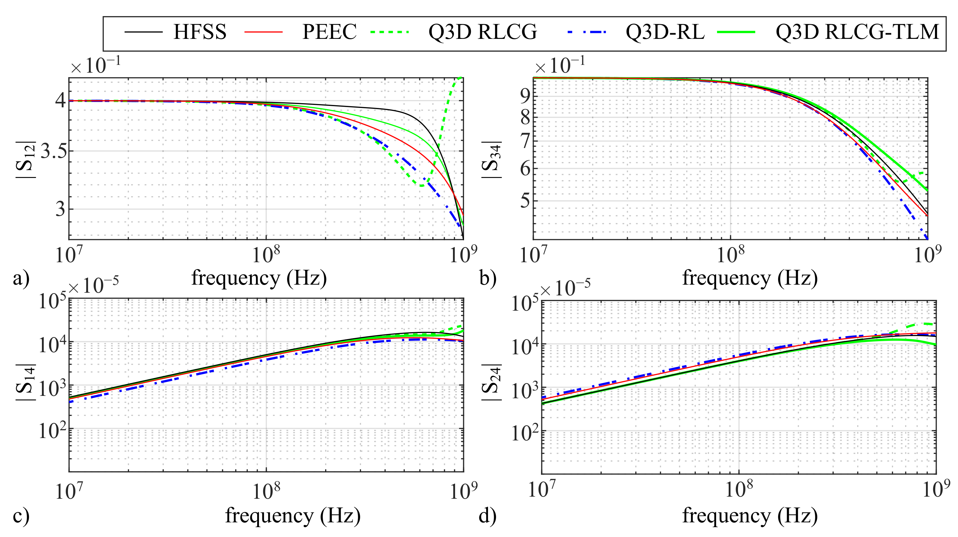
3.3.3. Resulting S-Parameters

The S-parameters were first calculated by the in-house developed PEEC solver, the HFSS 3-D FEM solver, the Q3D RLCG-solver and Q3D RL-solver. They are shown in Figure 4. In the Q3D, S-parameters can be calculated either by an equivalent TLM or a lumped RLGC model. The TLM distributes the lumped resistances (R), inductances (L), conductances (G) and capacitances (C) uniformly across a system of coupled transmission lines, which corresponds to adding more internal nodes in between the input modeling nodes. The S-parameters, S 12 , S 14 , S 34 , and S 24 , are selected to show the differences between the modeling approaches. S 14 and S 24 contribute to the gate-power loops coupling, while S 12 and S 34 are associated to the power loop impedance and the gate loop impedance, respectively. In the HF range, the PEEC S-parameters are physically more closer to the HFSS S-parameters than the Q3D RLCG S-parameters. To fully match the PEEC and HFSS S-parameters is challenging mainly due to the PEEC mesh requirements.
As explained in Section 3.2, the TLM can increase accuracy for certain modeling structures in power electronics. Using the Q3D RLCG model, the S 12 and S 34 show a higher deviation from the S-parameters calculated by the HFSS 3-D FEM solver and the PEEC solver, as it can be seen in Figure 4a,b, respectively. In particular, the accuracy of S 12 and S 34 is improved by using the Q3D RLCG-TLM, while the S 14 and S 24 , shown in Figure 4c,d, calculated by the Q3D RLCG-TLM show still a visible deviation from the corresponding HFSS and PEEC S-parameters in the HF range above 100 MHz . The effects of electric-field induced couplings can be identified by comparing the Q3D-RLCG and Q3D-RL S-parameters.
The importance of these differences observed in the S-parameters calculated by five different methods is evaluated by modeling the switching transients of power MOSFETs as shown in the next section.

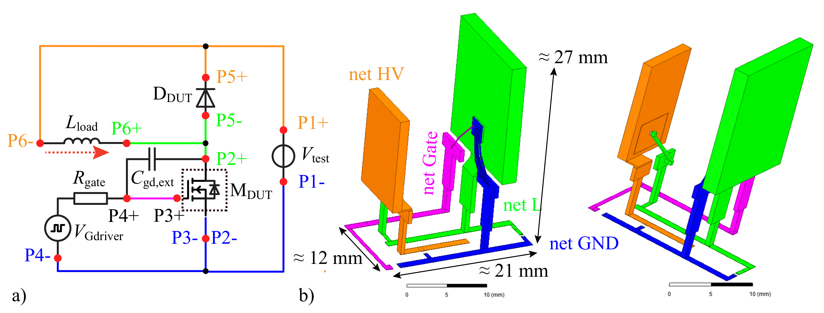
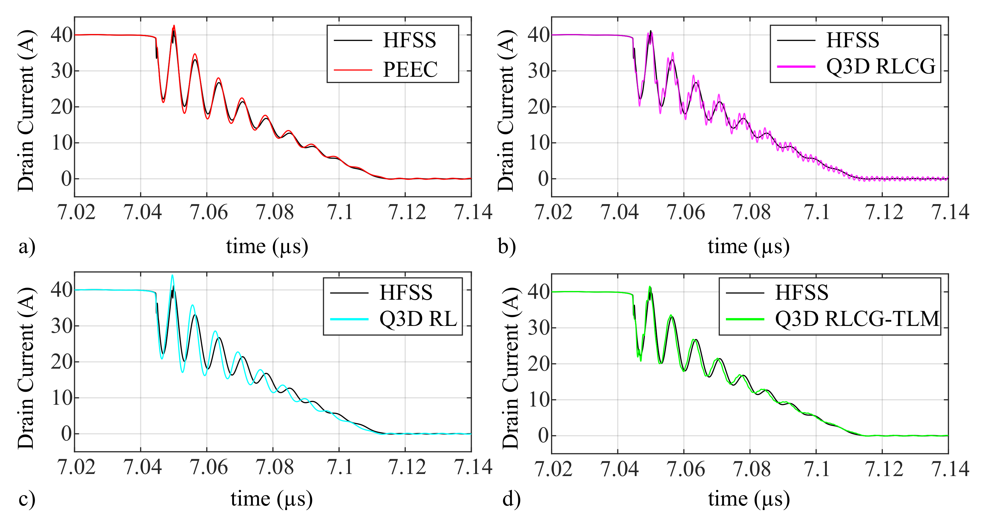
4. Device-Circuit Layout Coupled Simulations

The aim of this section is to demonstrate the main differences between three numerical techniques with respect to predicting fast switching transients of power semiconductor devices, such as Si Super Junction (SJ) and SiC power MOSFETs. The potential differences between switching transient simulations are demonstrated on two examples, implementing the EM macromodels, i.e., S 6 × 6 parameters, as extracted by the PEEC solver developed in-house, and the commercial tools ANSYS Q3D and HFSS (see above). The current commutation between a SiC diode D DUT (IDWD40G120C5) [42] and a power MOSFET M DUT is simulated in ANSYS Nexxim using the DPT circuit shown in Figure 2. As layout optimization is crucial for achieving the best performance of fast switching power devices, M DUT is in the first example modeled as a fast switching high efficiency Si SJ power MOSFET (IPP60R180C7), M DUT 1 , Ref. [43] and in the second example as a SiC trench power MOSFET (IMZ120R030M1H) [44] ( M DUT 2 ), using the vendor-provided Spice models.

4.1. Example 1

The first example demonstrates the simulation of HF oscillations in the power loop amplified from the gate loop oscillations via the high transconductance of the MOSFET, i.e., i d g m V gs modeling M DUT 1 as a 600 V , 180 m Ω fast switching Si SJ power MOSFET. The current waveforms simulated in ANSYS Nexxim using the DPT circuit from Figure 2a with the PEEC-, Q3D- and HFSS- S 6 × 6 parameters are shown in Figure 5 for M DUT 1 switching the current I L = 40 A at V test = 400 V for R gate = 2 Ω and C gd , ext = 10 pF .
The detailed comparison of the drain current, i d , waveforms in Figure 6a demonstrates the main differences of three numerical techniques.
A good matching between the transient simulations with the PEEC- and HFSS- 6 × 6 S-parameters, cf. Figure 5a and Figure 6a, points out that the QS field assumption used by the PEEC solver is still valid. The S 6 × 6 parameters extracted by the Q3D RLCG solvers with and without the TLM introduce HF ringing of the drain current, which is not observed in the transient simulations using the PEEC- and HFSS- S 6 × 6 parameters, see Figure 5b,d and Figure 6a. By using the S 6 × 6 parameters from Q3D-RL Solver, the i d waveform does not contain the HF ringing, however, a mismatch to the i d waveform simulated with the HFSS S 6 × 6 parameters is visible, cf. Figure 5c. Comparing the i d waveforms at the beginning of the current switching transient as shown in Figure 7a, it can be observed that the S 6 × 6 parameters from the Q3D-RL solver, not modeling electric field effects, do not capture the first current valleys modeled by the PEEC- and HFSS-S 6 × 6 parameters, while the Q3D RLCG- and Q3D RLCG-TLM-S 6 × 6 parameters introduce additional HF oscillations. The differences of the EM modeling approaches can quantitatively evaluated by comparing the spectra of the turn-off current waveforms as shown in Figure 6b. The Q3D RLCG model leads to higher amplitude harmonics around 600 MHz 700 MHz , which is shifted towards 800 MHz 1 GHz and reduced by using the TLM approach. Accordingly, the TLM improves the accuracy of the Q3D RLCG modeling in a wider frequency range, however the distributed RLCG coupled transmission line system set automatically by the Q3D, does not eliminate all HF inaccuracies. Taking the current spectrum simulated by the HFSS-S 6 × 6 parameters as reference, the maximum errors of the spectra simulated by the 3-D PEEC-, the Q3D RLCG-, the Q3D RLCG-TLM- and the Q3D RL-S 6 × 6 parameters are 14.1 % , 32.6 % , 33.5 % and 18.3 % , respectively.

4.2. Example 2

The second example presents the current switching waveforms of a 1.2 kV , 30 m Ω SiC trench power MOSFET containing HF ringing mainly caused by the layout parasitics. The transient current switching waveforms simulated using different S 6 × 6 parameters and their spectra are shown in Figure 7 and Figure 8. The comparison in Figure 7a and Figure 8a shows that the transient simulations with the PEEC- and HFSS-S 6 × 6 parameters capture the same resonance frequency of HF oscillations of ≈ 98 MHz but with different amplitudes. This leads to higher amplitude of HF harmonics in the spectrum calculated by the 3-D PEEC-S 6 × 6 parameters in comparison to the spectrum of the HFSS-S 6 × 6 parameters. To better match the 3-D PEEC modeling with HFSS 3-D FEM modeling, an optimized non-uniform meshing is required. On the other hand, the transient simulations with the S 6 × 6 parameters extracted by the Q3D RLCG and RL solvers contain the HF oscillations shifted by ≈ 2 MHz in the resonant frequency, cf. Figure 7b,c. The S 6 × 6 parameters extracted by the Q3D RLCG solver, cf. Figure 7b, additionally contribute to a higher damping that can be attributed to higher capacitive effects modeled by the Q3D-RLCG S-parameters. The TLM improves the Q3D RLCG modeling, however, similarly to the previous example, the spectra calculated by the Q3D RLCG with and without TLM both show high amplitude harmonics in the HF range not observed in the spectra calculated by HFSS 3-D FEM, Q3D RL, and 3-D PEEC methods. Taking the current spectrum simulated by the HFSS-S 6 × 6 parameters as reference, the maximum errors of the spectra simulated by the 3-D PEEC-, the Q3D RLCG-, the Q3D RLCG-TLM- and the Q3D RL-S 6 × 6 parameters are 39 % , 74 % , 75 % and 51 % , respectively.

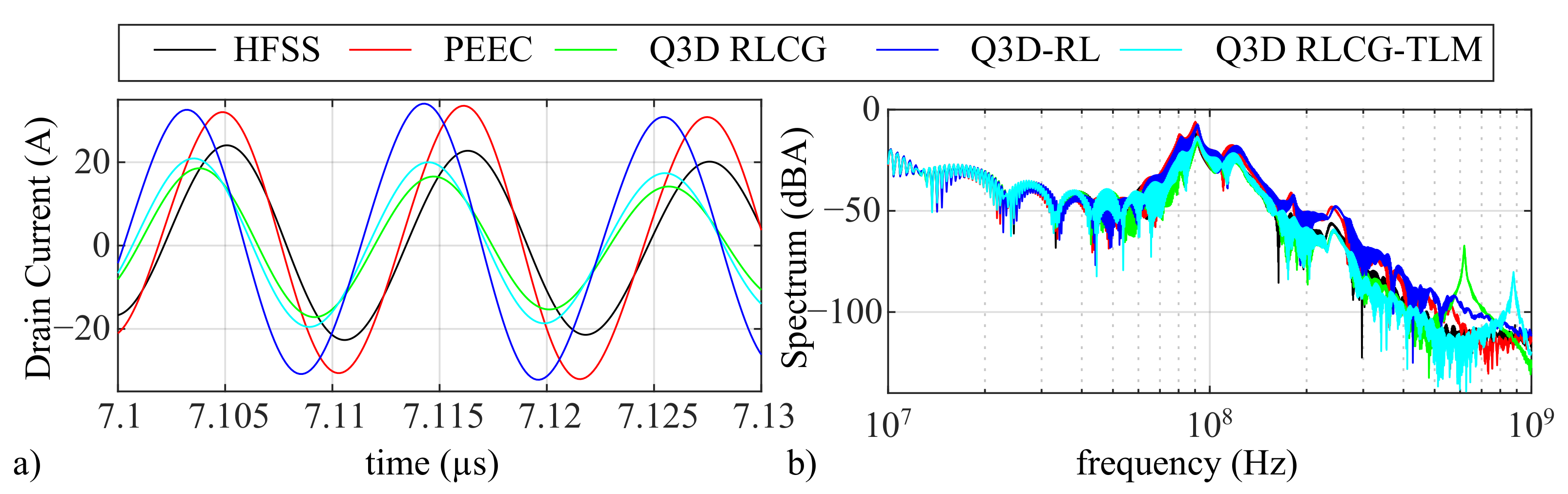
4.3. Results Analysis

The differences observed in the transient simulations of the MOSFET drain current using the two examples described above demonstrate the capabilities of three numerical techniques, the FEM, the equivalent-RLCG-circuit method, and the PEEC method, used in computational electromagnetics for PE applications. Similarly to [22], the performed analysis also points out that consideration of the broadband frequency range is necessary for accurately capturing the fast switching transitions of modern power devices. Namely, under the QS field assumption, which can be assumed for a large number of PE applications, it is shown that the PEEC-based EM modeling can be as accurate as the well-established FEM-based EM modeling. The frequency range up to hundreds of MHz is important for accurate simulations of PE circuits and their layouts. The RLCG-equivalent-circuit-based methods have to be used carefully since here the modeling of electric-field induced coupling effects is approximated in comparison to the 3-D PEEC modeling, leading to pronounced artificial oscillations and/or overestimation of capacitive effects. As long as a layout features dominantly inductive behavior, the modeling using the Q3D RL-solver, the PEEC solver, and the HFSS 3-D FEM solver is behaving more similar. To accurately capture HF ringing behavior originating from both magnetic and electric field coupling effects often occuring in the switching transients of power semiconductor device due to layout parasitics, the FEM-based or the PEEC-based EM solvers represent a better alternative than the RLCG-equivalent circuit EM solvers.

5. Conclusions

This paper shows the capabilities of three numerical techniques, the PEEC method, the HFSS 3-D FEM, and the Q3D RLCG-equivalent-circuit method typically used for broadband EM modeling of PES. Special attention is given to the differences between the QS 3-D PEEC- and the RLCG-equivalent-circuit-based EM modeling, which have been frequently overlooked so far. The HFSS 3-D FEM solver has a high potential for modeling broadband EM behavior of power converters. However, the FEM-based EM solvers require that the ports are small in size and referenced to a common return current path. Here, in general, the PEEC method offers a higher flexibility in setting-up of the ports. In addition, the commercial FEM-based EM solvers are typically optimized for either LF or HF EM simulations, whereas the required accuracy of broadband EM modeling depends on the application. The broadband capabilities and accuracy of the PEEC method are shown on a modeling example of a 3-D structure rather simplified in comparison to circuit layout geometries in real applications. This is mainly do to the present difficulties with automatized PEEC meshing of more complex structures. Consequently, the current on-going research on the PEEC method is focusing on the development of a PEEC mesher which can automatically handle more complex geometries, and a broadband surface-based PEEC formulation for capturing HF effects at lower computational costs.

Author Contributions

Conceptualization, I.K.-B., D.R., G.A., J.E., and U.G.; methodology, I.K.-B., D.R., G.A., J.E., and U.G.; software, I.K.-B., and D.R.; validation, I.K.-B., and D.R.; formal analysis, I.K.-B., D.R., G.A., J.E., and U.G.; investigation, I.K.-B., D.R., G.A.; resources, I.K.-B., D.R., G.A., J.E., and U.G.; data curation, I.K.-B., and D.R.; writing–original draft preparation, I.K.-B.; writing–review and editing, I.K.-B., D.R., G.A., J.E., and U.G.; visualization, I.K.-B.; supervision, I.K.-B.; project administration, I.K.-B.; funding acquisition, U.G. All authors have read and agreed to the published version of the manuscript.

Funding

This research received no external funding.

Conflicts of Interest

The authors declare no conflict of interest.

Abbreviations

The following abbreviations are used in this manuscript:
MDPIMultidisciplinary Digital Publishing Institute
DOAJDirectory of open access journals
EMElectromagnetic
PEPower electronics
PESPower electronic systems
HFHigh Frequency
LFLow Frequency
SiCSilicon Carbide
PEECPartial Element Equivalent Circuit
FEMFinite Element Method
3-Dthree-dimensional

References

  1. Liu, T.; Wong, T.T.; Shen, Z.J. A new characterization technique for extracting parasitic inductances of SiC power MOSFETs in discrete and module packages based on two-port S-parameters measurement. IEEE Tran. Power Electron. 2018, 33, 9819–9833. [Google Scholar] [CrossRef]
  2. Lemmon, A.; Graves, R. Parasitic extraction procedure for silicon carbide power modules. In Proceedings of the 2015 IEEE International Workshop on Integrated Power Packaging (IWIPP), Chicago, IL, USA, 3–6 May 2015; pp. 91–94. [Google Scholar]
  3. Shahabi, A.; Lemmon, A.N. Multibranch Inductance Extraction Procedure for Multichip Power Modules. IEEE J. Emerg. Sel. Top. Power Electron. 2020, 8, 272–285. [Google Scholar] [CrossRef]
  4. Mukunoki, Y.; Nakamura, Y.; Konno, K.; Horiguchi, T.; Nakayama, Y.; Nishizawa, A.; Kuzumoto, M.; Akagi, H. Modeling of a SiC MOSFET with focus on internal stray capacitances and inductances, and its verification. IEEE Tran. Ind. Appl. 2018, 54, 2588–2597. [Google Scholar] [CrossRef]
  5. Pace, L.; Defrance, N.; Videt, A.; Idir, N.; De Jaeger, J.C.; Avramovic, V. Extraction of Packaged GaN Power Transistors Parasitics Using S-Parameters. IEEE Tran. Electron. Devices 2019, 66, 2583–2588. [Google Scholar] [CrossRef]
  6. Iida, H.; Hasegawa, K.; Omura, I. Mutual inductance influence to switching speed and TDR measurements for separating self-and mutual inductances in the package. In Proceedings of the 31st International Symposium on Power Semiconductor Devices and ICs (ISPSD), Shanghai, China, 19–23 May 2019; pp. 503–506. [Google Scholar]
  7. Kovacevic-Badstuebner, I.; Grossner, U.; Popescu, D. Tools for Broadband Electromagnetic Modeling of Power Semiconductor Packages and External Circuit Layouts. In Proceedings of the 32nd International Symposium on Power Semiconductor Devices and ICs (ISPSD), Vienna, Austria, 13–18 September 2020; pp. 388–391. [Google Scholar] [CrossRef]
  8. Popescu, D.; Treiber, M. Broadband TCAD mixed-mode simulation framework for predictive modeling of fast dynamic switching events. In Proceedings of the 31st Int. Sym. on Power Semiconductor Devices and ICs (ISPSD), Shanghai, China, 19–23 May 2019; pp. 327–330. [Google Scholar]
  9. Le, Q.; Evans, T.; Peng, Y.; Mantooth, H.A. PEEC Method and Hierarchical Approach Towards 3D Multichip Power Module (MCPM) Layout Optimization. In Proceedings of the IEEE International Workshop on Integrated Power Packaging (IWIPP), Toulouse, France, 24–26 April 2019; pp. 131–136. [Google Scholar] [CrossRef]
  10. Che, C.; Zhao, H.; Guo, Y.; Hu, J.; Kim, H. Investigation of Segmentation Method for Enhancing High Frequency Simulation Accuracy of Q3D Extractor. In Proceedings of the IEEE International Conference on Computational Electromagnetics (ICCEM), Shanghai, China, 20–22 March 2019; pp. 1–3. [Google Scholar] [CrossRef]
  11. Jorgensen, A.B.; Munk-Nielsen, S.; Uhrenfeldt, C. Overview of Digital Design and Finite-Element Analysis in Modern Power Electronic Packaging. IEEE Trans. Power Electron. 2020, 35, 10892–10905. [Google Scholar] [CrossRef]
  12. Zeng, Y.; Yi, Y.; Liu, P. An Improved Investigation into the Effects of the Temperature-Dependent Parasitic Elements on the Losses of SiC MOSFETs. Appl. Sci. 2020, 10, 7192. [Google Scholar] [CrossRef]
  13. Gabriadze, G.; Chiqovani, G.; Gheonjian, A.; Oganezova, I.; Demurov, A.; Kutchadze, Z.; Bunlon, X.; Ajebbar, F.; Jobava, R. Enhanced PEEC Model Based on Automatic Voronoi Decomposition of Triangular Meshes. IEEE Trans. Electromagn. Compat. 2020, 62, 2196–2208. [Google Scholar] [CrossRef]
  14. Liu, H.; Huang, X.; Lin, F.; Yang, Z. Loss Model and Efficiency Analysis of Tram Auxiliary Converter Based on a SiC Device. Energies 2017, 10, 2018. [Google Scholar] [CrossRef] [Green Version]
  15. Alimeling, J.H.; Hammer, W.P. PLECS-piece-wise linear electrical circuit simulation for Simulink. In Proceedings of the IEEE 1999 International Conference on Power Electronics and Drive Systems. PEDS’99 (Cat. No.99TH8475), Hong Kong, China, 27–29 July 1999; Volume 1, pp. 355–360. [Google Scholar] [CrossRef]
  16. Muesing, A.; Kolar, J.W. Successful online education—GeckoCIRCUITS as open-source simulation platform. In Proceedings of the 2014 International Power Electronics Conference (IPEC-Hiroshima 2014—ECCE ASIA), Hiroshima, Japan, 18–21 May 2014; pp. 821–828. [Google Scholar] [CrossRef]
  17. Stark, R.; Tsibizov, A.; Nain, N.; Grossner, U.; Kovacevic-Badstuebner, I. Accuracy of Three Inter-Terminal Capacitance Models for SiC Power MOSFETs under Fast Switching. IEEE Trans. Power Electron. 2021. [Google Scholar] [CrossRef]
  18. Triverio, P.; Grivet-Talocia, S.; Nakhla, M.S.; Canavero, F.G.; Achar, R. Stability, Causality, and Passivity in Electrical Interconnect Models. IEEE Trans. Adv. Packag. 2007, 30, 795–808. [Google Scholar] [CrossRef] [Green Version]
  19. Romano, D.; Antonini, G.; Grossner, U.; Kovacvic-Badstuebner, I. Circuit synthesis techniques of rational models of electromagnetic systems: A tutorial paper. Int. J. Numer. Model. Electron. Netw. Devices Fields 2019, 32. [Google Scholar] [CrossRef]
  20. Gustavsen, B.; Semlyen, A. Rational approximation of frequency domain responses by vector fitting. IEEE Trans. Power Deliv. 1999, 14, 1052–1061. [Google Scholar] [CrossRef] [Green Version]
  21. Ekman, J. Electromagnetic Modeling Using the Partial Element Equivalent Circuit Method. Ph.D. Thesis, Lulea University of Technology, Lulea, Sweden, 2003. [Google Scholar]
  22. Schroeder, A.; Wunsch, B.; Kicin, S. Wideband Macro-Modelling of Power Modules for Transient Electromagnetic Analysis. In Proceedings of the 11th International Conference on Integrated Power Electronics Systems (CIPS), Berlin, Germany, 24–26 March 2020; pp. 1–5. [Google Scholar]
  23. Ruehli, A.E.; Antonini, G.; Jiang, L. Circuit Oriented Electromagnetic Modeling Using the PEEC Techniques; John Wiley & Sons, Inc.: Hoboken, NJ, USA, 2017. [Google Scholar]
  24. Ho, A. Ruehli, P. Brennan, C. The modified nodal approach to network analysis. IEEE Trans. Circuits Syst. 1975, 22, 504–509. [Google Scholar]
  25. Hartman, A.; Romano, D.; Antonini, G.; Ekman, J. Partial Element Equivalent Circuit Models of Three-Dimensional Geometries Including Anisotropic Dielectrics. IEEE Trans. Electromagn. Compat. 2018, 60, 696–704. [Google Scholar] [CrossRef]
  26. Kovacevic-Badstuebner, I.; Romano, D.; Antonini, G.; Lombardi, L.; Grossner, U. Full-Wave Computation of the Electric Field in the Partial Element Equivalent Circuit Method Using Taylor Series Expansion of the Retarded Green’s Function. IEEE Trans. Microw. Theory Tech. 2020, 68, 3242–3254. [Google Scholar] [CrossRef]
  27. Nguyen, T.S.; Duc, T.L.; Tran, T.S.; Guichon, J.M.; Chadebec, O.; Meunier, G. Adaptive Multipoint Model Order Reduction Scheme for Large-Scale Inductive PEEC Circuits. IEEE Trans. Electromagn. Compat. 2017, 59, 1143–1151. [Google Scholar] [CrossRef]
  28. Romano, D.; Antonini, G. Partitioned Model Order Reduction of Partial Element Equivalent Circuit Models. IEEE Trans. Components, Packag. Manuf. Technol. 2014, 4, 1503–1514. [Google Scholar] [CrossRef]
  29. Kamon, M.; Tsuk, M.; White, J. FASTHENRY: A multipole-accelerated 3-D inductance extraction program. IEEE Trans. Microw. Theory Tech. 1994, 42, 1750–1758. [Google Scholar] [CrossRef]
  30. Vialardi, E.; Clavel, E.; Chadebec, O.; Guichon, J.M.; Lionet, M. Electromagnetic simulation of power modules via adapted modelling tools. In Proceedings of the 14th International Power Electronics and Motion Control Conference (EPE-PEMC), Ohrid, Macedonia, 6–8 September 2010; pp. T2-78–T2-83. [Google Scholar] [CrossRef] [Green Version]
  31. Nabors, K.; White, J. FastCap: A multipole accelerated 3-D capacitance extraction program. IEEE Trans. Comput. Aided Des. Integr. Circuits Syst. 1991, 10, 1447–1459. [Google Scholar] [CrossRef] [Green Version]
  32. Cottet, D.; Paakkinen, M. Scalable PEEC-SPICE modelling for EMI analysis of power electronic packages and subsystems. In Proceedings of the 8th Electronics Packaging Technology Conference, Singapore, 6–8 December 2006; pp. 871–878. [Google Scholar] [CrossRef]
  33. Ardon, V.; Aime, J.; Chadebec, O.; Clavel, E.; Guichon, J.M.; Vialardi, E. EMC Modeling of an Industrial Variable Speed Drive With an Adapted PEEC Method. IEEE Trans. Magn. 2010, 46, 2892–2898. [Google Scholar] [CrossRef] [Green Version]
  34. Rondon-Pinilla, E.; Morel, F.; Vollaire, C.; Schanen, J.L. Modeling of a Buck Converter With a SiC JFET to Predict EMC Conducted Emissions. IEEE Trans. Power Electron. 2014, 29, 2246–2260. [Google Scholar] [CrossRef] [Green Version]
  35. Musing, A.; Heldwein, M.L.; Friedli, T.; Kolar, J.W. Steps Towards Prediction of Conducted Emission Levels of an RB-IGBT Indirect Matrix Converter. In Proceedings of the Power Conversion Conference (PCC), Nagoya, Japan, 2–5 April 2007; pp. 1181–1188. [Google Scholar] [CrossRef]
  36. Evans, P.L.; Castellazzi, A.; Johnson, C.M. Design Tools for Rapid Multidomain Virtual Prototyping of Power Electronic Systems. IEEE Trans. Power Electron. 2016, 31, 2443–2455. [Google Scholar] [CrossRef]
  37. Kovacevic-Badstuebner, I.; Grossner, U.; Romano, D.; Antonini, G.; Ekman, J. A more accurate electromagnetic modeling of WBG power modules. In Proceedings of the IEEE 30th International Symposium on Power Semiconductor Devices and ICs (ISPSD), Chicago, IL, USA, 13–17 May 2018; pp. 260–263. [Google Scholar] [CrossRef]
  38. Kovacevic-Badstuebner, I.; Romano, D.; Lombardi, L.; Grossner, U.; Ekman, J.; Antonini, G. Accurate Calculation of Partial Inductances for the Orthogonal PEEC Formulation. IEEE Trans. Electromagn. Compat. 2021, 63, 82–92. [Google Scholar] [CrossRef]
  39. Ruehli, A.E.; Antonini, G.; Esch, J.; Ekman, J.; Mayo, A.; Orlandi, A. Nonorthogonal PEEC formulation for time- and frequency-domain EM and circuit modeling. IEEE Trans. Electromagn. Compat. 2003, 45, 167–176. [Google Scholar] [CrossRef] [Green Version]
  40. Kovacevic-Badstuebner, I.; Stark, R.; Grossner, U.; Guacci, M.; Kolar, J.W. Parasitic Extraction Procedures for SiC Power Modules. In Proceedings of the 10th International Conference on Integrated Power Electronics Systems (CIPS), Stuttgart, Germany, 20–22 March 2018; pp. 1–6. [Google Scholar]
  41. Sun, W. Accurate EM simulation of SMT components in RF designs. In Proceedings of the IEEE Radio Frequency Integrated Circuits Symposium (RFIC), Honolulu, HI, USA, 4–6 June 2017; pp. 140–143. [Google Scholar] [CrossRef]
  42. Infineon. 5th Generation CoolSiC 1200V Schottky Diode (IDWD40G120C5). Available online: https://www.infineon.com/dgdl/Infineon-IDWD40G120C5-DataSheet-v02_00-EN.pdf?fileId=5546d462689a790c016933d56ffd548f (accessed on 14 May 2021).
  43. Infineon. CoolMOS C7 600 V PowerTransistor (IPP60R180C7). Available online: https://www.infineon.com/dgdl/Infineon-IPP60R180C7-DS-v02_00-EN.pdf?fileId=5546d4624cb7f111014d483fe4ba707b (accessed on 14 May 2021).
  44. Infineon. CoolSiC 1200V SiC Trench MOSFET Silicon Carbide MOSFET (IMZ120R030M1H). Available online: https://www.infineon.com/dgdl/Infineon-IMZ120R030M1H-DataSheet-v02_02-EN.pdf?fileId=5546d46269e1c019016a92fdcc776696 (accessed on 14 May 2021).
Figure 1. Diagram showing the state-of-the-art device-circuit layout modeling.
Energies 14 02835 g001
Figure 2. EM modeling of fast switching transients based on a DPT circuit: (a) the DPT circuit schematic with marked connected areas and 12 ports, (b) 3D circuit layout including PCB tracks and two TO-packages for a free-wheeling diode and a power switch.
Energies 14 02835 g002
Figure 3. PEEC meshing procedure: (a) cutting the 3-D modeling domain, and (b) meshing.
Energies 14 02835 g003
Figure 4. The magnitude of selected S parameters calculated in the HF range by the PEEC solver developed in-house, the HFSS 3-D FEM solver, the Q3D RLCG-solver, the Q3D RLCG-solver with TLM, and the Q3D RL-solver: (a) S 12 , (b) S 14 , (c) S 34 and (d) S 24 .
Energies 14 02835 g004
Figure 5. Simulations of HF oscillations observed in the drain current waveform of a fast switching Si SJ power MOSFET M DUT 1 for I L = 40 A , V test = 400 V , R gate = 2 Ω , C gd , ext = 10 pF using the extracted S 6 × 6 parameters: (a) HFSS vs. PEEC, (b) HFSS vs. Q3D RLCG, (c) HFSS vs. Q3D RL, and (d) HFSS vs. Q3D RLCG-TLM.
Energies 14 02835 g005
Figure 6. Detailed comparison of current waveforms shown on Figure 5: (a) the zoom of all waveforms at the beginning of the switching transition, and (b) the spectrum of turn-off current waveforms.
Energies 14 02835 g006
Figure 7. Simulations of HF oscillations observed in the drain current waveform of a SiC trench power MOSFET M DUT 2 for I L = 40 A , V test = 600 V , R gate = 1 Ω , C gd , ext = 1 pF using the extracted 6 × 6 S-parameters: (a) HFSS vs. PEEC, (b) HFSS vs. Q3D RLCG, (c) HFSS vs. Q3D RL, and (d) HFSS vs. Q3D RLCG-TLM.
Energies 14 02835 g007
Figure 8. Detailed comparison of current waveforms shown on Figure 7: (a) the zoom of all waveforms at the beginning of the switching transition, and (b) the spectrum of current switching waveforms.
Energies 14 02835 g008
Publisher’s Note: MDPI stays neutral with regard to jurisdictional claims in published maps and institutional affiliations.

