1. Introduction
Transformerless threephase, twolevel architectures are widely used for power converters due to their good harmonic characteristics; however, they exhibit poor common-mode performance.
The problem of common-mode currents (CMCs) is a very sensitive issue in electric drives. Rapidly varying PWM-frequency common-mode voltages (CMVs) at the output of an inverter cause common-mode currents to flow through the usually capacitive common-mode paths that exist between the inverter and the ground. This may lead to partial discharges, faults, and electromagnetic interference (EMI) that in turn can cause the inverter control to trip [
1,
2].
One of the most common paths for CMCs in electric motor drives is through the shaft bearings, because of the parasitic capacitance between stator and rotor [
3]. CMCs can damage the bearings causing premature motor failure. This problem has been thoroughly studied and modeled [
4,
5], and many solutions have been proposed to reduce or compensate for its effects, including common-mode transformers [
6] and active filters [
7,
8].
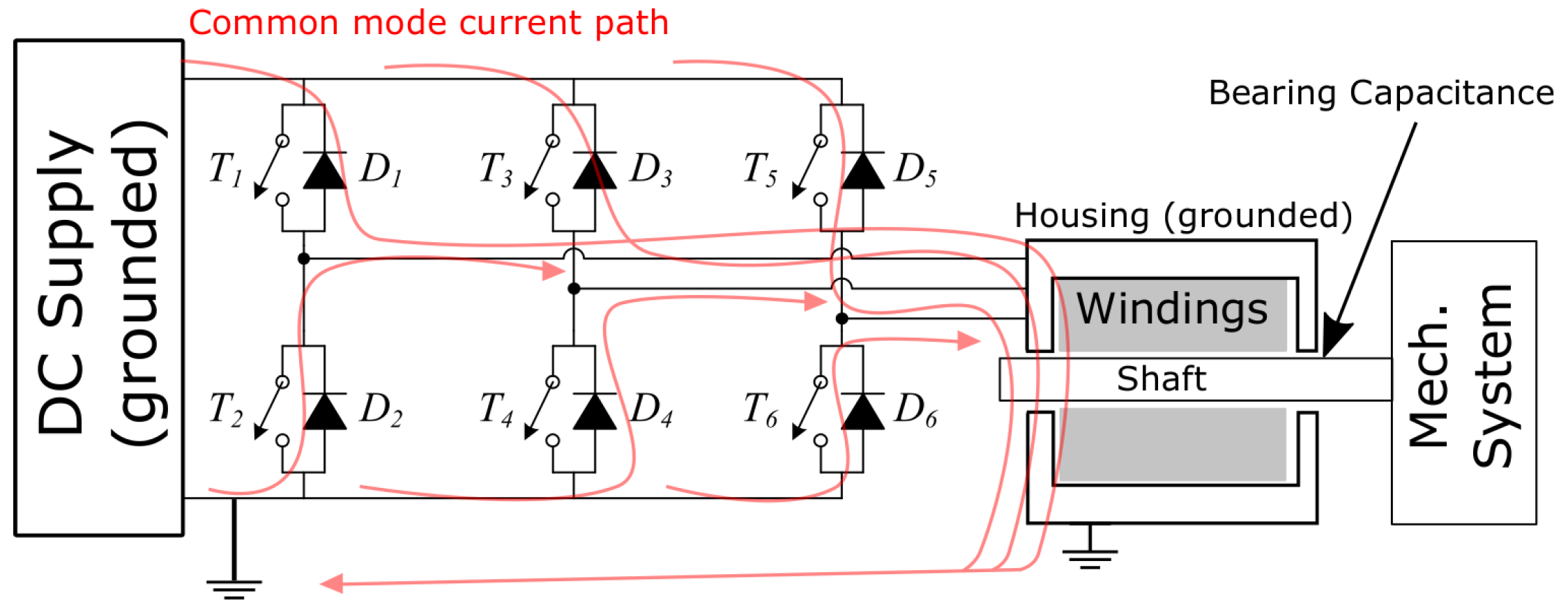
In automotive traction drives, CMCs are the source of EMI and possible resonance phenomena [
9]. Possible return current paths include the braided shield of the motor cable, the metallic vehicle body and parasitic capacitance among the vehicle components [
10], as shown in
Figure 1, where the common mode current path is highlighted for a three-phase full-bridge electrical drive. These problems can be mitigated by suitable mechanical packaging and cable routing [
11] and by shielding and isolating the traction system from the vehicle chassis, although this will not protect the motor bearings from suffering the effects of CMCs [
12].
For the above reasons, researchers have been active in finding new solutions to reduce this undesired current, and reducing the common mode voltage variation is one of the most investigated solutions. In fact, the leakage current is proportional to the voltage derivative over the parasitic capacitance in the common-mode circuit.
Wide-bandgap devices and the consequent increase of the operating frequency of converters is increasing performance [
13] and reliability [
14], but it is also making CMV reduction even more necessary [
15].
This paper explores the performance of a three-phase converter named H8 [
16,
17] with the focus on motor drive application. Different semiconductors and modulation strategies are evaluated having the three-phase full-bridge (H6) architecture as a benchmark.
2. Modulations for Common-Mode Voltage Mitigation
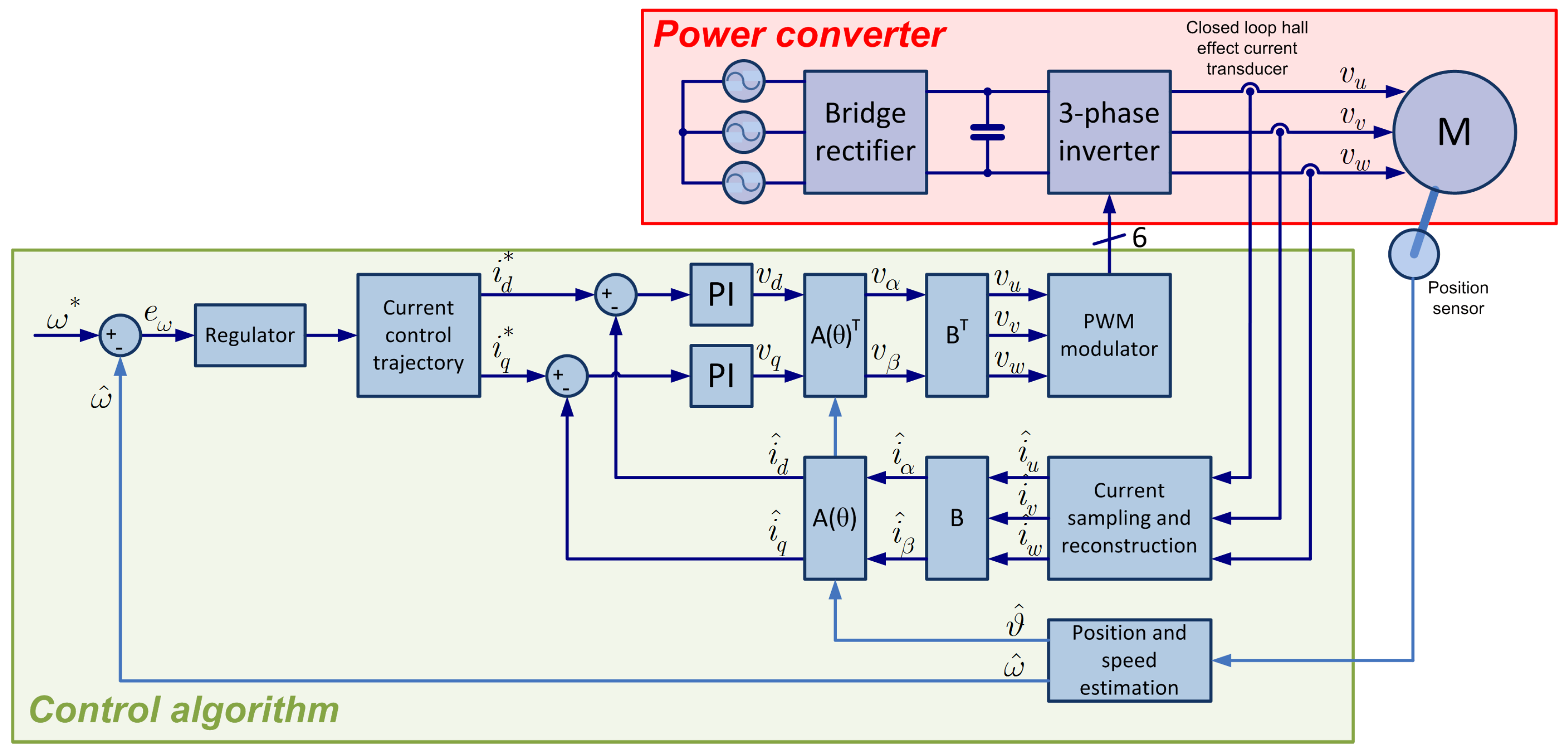
Figure 2 shows the general layout of an electric motor drive. The type of the motor is not specified, as the scheme has a general validity. The “Current control trajectory” block is customized depending on the kind of the machine: Surface Permanent Magnet machines (SPM) would normally feature a zero direct current, whereas Internal Permanent Magnet (IPM) as well as Synchronous Reluctance machines (SRM) would have an optimized current reference generation. Induction machines would also have an additional control loop for the control of the flux.
The energy flow between source and mechanical output is normally controlled by the combination of a power electronic converter, where the control of the energy flow actually occurs, and an electromechanical converter, i.e., an electrical machine, that acts as drive mechanism. Basically, the utility input is rectified by means of either a controlled or an uncontrolled rectifier and then converted again into AC to supply the motor with a three-phase voltage adjusted in magnitude and frequency using a modulation technique. A battery can be used instead of the utility grid to provide the DC link. The direct connection of the battery to the metallic chassis of the car and the machine bearing and parasitic capacitance to the housing would constitute the common-mode path.
Space vector PWM (SVPWM) is the most common kind of modulation for coping with this problem. A constant CMV is not difficult to obtain in principle: it suffices to only use states having the same CMV. Nevertheless, this approach has its own drawbacks, that in some cases prevent its use. Many authors have pursued a reduction of the CMV employing variations of the basic SVPWM [
18,
19,
20]. In principle, each technique has its own drawbacks, like distortion, partial elimination of the CMV [
19], or increased current ripple. This section reports a brief survey of existing reduced CMV PWMs (RCMV-PWM).
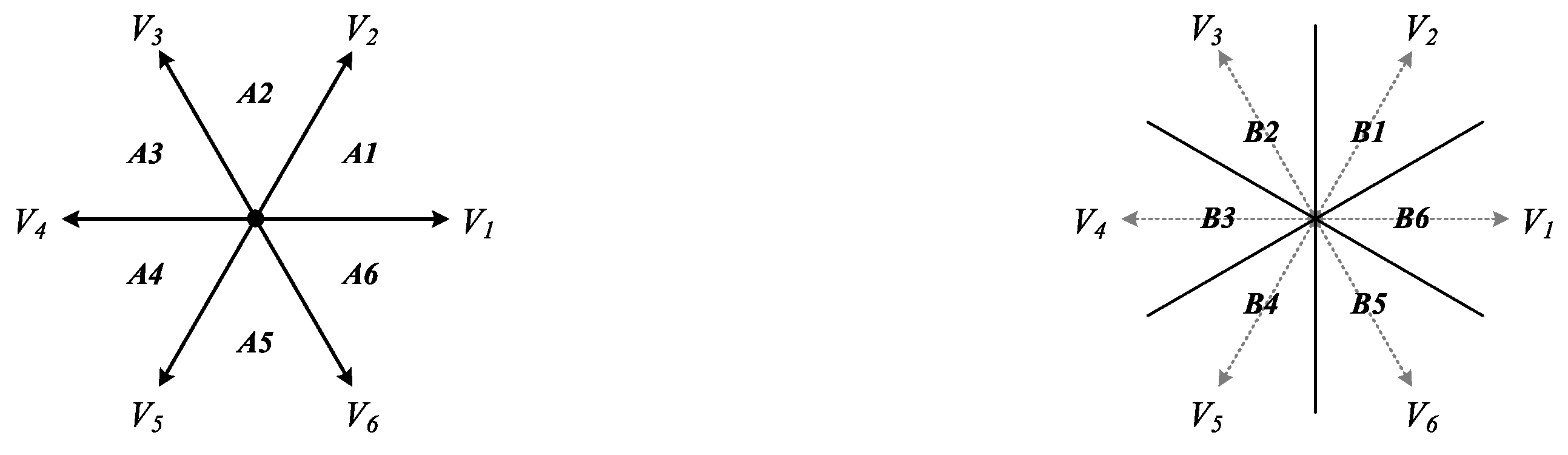
Unlike SVPWM, which uses of all the possible space vectors, RCMV-PWM methods employ only subsets of the active ones [
19]. These methods are briefly described in the following, while vector patterns for each are listed in
Table 1 considering the operating regions defined in
Figure 3.
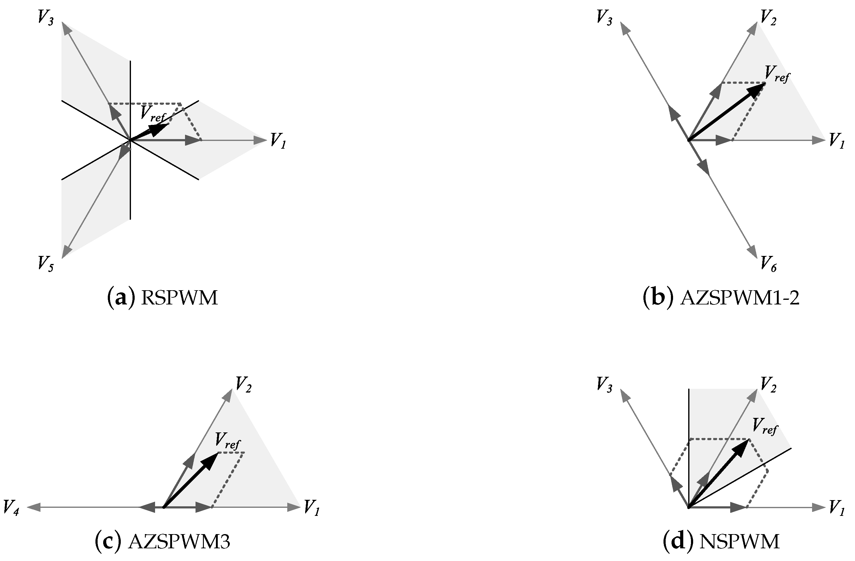
Active Zero-State (AZSPWM): two opposite active vectors are used in place of the zero-voltage vectors and . Three variations on this idea (AZSPWM1-3) can be found in literature; they differ in the adoption of different combinations of opposite vectors.
Remote States (RSPWM): this method uses three active vectors 120° apart. Two groups are determined (-- and --) and, within each group, different vector sequences can be chosen. Four variations can be found in literature for this type of modulation, referred to as RSPWM1, RSPWM2A, RSPWM2B, and RSPWM3.
Near States (NSPWM): given a reference, the closest voltage vector and its two neighbors are used. They are sequenced to minimize the number of switching events. Within each sampling interval there is one of the bridge legs undergoing zero switching events.
Discontinuous (DPWM): differs from regular SVPWM for using only one of the two zero states; therefore, CMV undergoes one less step of variation.
Each RCMV-PWM technique yields different frequency and polarity of CMV. RSPWM1 and RSPWM2 have theoretically no CMV variation, which is the most favorable condition. In RSPWM3, CMV is constant for each 60° interval. With AZSPWM2 and AZSPWM3, the CMV has the same frequency as the PWM, but with smaller steps relative to SVPWM. All the other techniques have higher CMV frequency and/or step size, therefore they are less attractive. SVPWM, AZSPWM1, DPWM1, and NSPWM result in inverter legs switching one at a time, while all the other RCMV-PWMs techniques determine simultaneous switching of two legs. This causes large (sometimes intolerably so) output ripple due to line-to-line output voltage reversals.
In conclusion, only NSPWM and AZSPWM1 are practical methods for reducing the CMV in two-level three-phase motor drives.
Figure 4 shows the output voltage generation of the different modulation strategies, highlighting the eligible voltage vectors. A reference voltage in the first sextant is considered and the length of the used vectors is proportional to the time they are applied.
3. Modulations for the H8 Architecture
The main idea behind the proposed H8 inverter is the reduction of the CMV by decoupling the AC and DC sides with power switches [
16]; this strategy has already been proven effective for single-phase photovoltaic inverters. A dedicated PWM technique was developed for CMV reduction alongside the proposed H8 architecture, exploiting the SVM degrees of freedom.
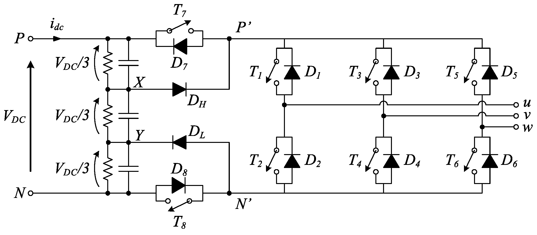
3.1. Architecture of the Converter
Figure 5 shows the H8 inverter architecture. Deriving from the traditional three-phase bridge structure (H6) with the addition of two switches, it was named “H8”. In addition to the two additional active devices, at the DC side, there is a network composed of a three-level voltage divider and two clamping diodes. The following subsections offer a detailed description of the added parts.
3.1.1. Voltage Divider
Three series capacitance form the DC Link, (
Figure 6a) with the purpose of obtaining intermediate voltage levels:
These two levels are useful to match the CMV values respectively during the odd (
,
,
) and even (
,
,
) active states, as will be further explained in
Section 3.2. In order to ensure a good partition of the voltage across the capacitors (i.e., not determined by their ESRs), three resistors were added in parallel to them and their value has to be as small as possible compatibly with their power losses.
3.1.2. DC Decoupling and Voltage Clamping
As shown in
Figure 6b, H8 includes two switching devices referred to as
and
which decouple the AC and DC path during the diode free-wheeling. On the contrary, during active states they are kept on, so to ensure the usual conduction path from the DC source to the inverter legs. In this condition they inevitably introduce on-state losses that detriment the overall efficiency of the converter. However, if they are chosen accurately, this drawback can still have an acceptable impact. As a matter of fact, the six H6 devices in the bridge must withstand the entire supply voltage, whereas across
and
only one third of it appears, so they can be chosen with a smaller breakdown voltage, which usually goes with smaller on-state resistance. It is also worth mentioning that, on the other hand, their current rating must be the same as the other six devices.
Moving to the diodes named and , the first is placed between the intermediate point of the divider X and the top bridge rail, labelled as ; reciprocally, the latter is placed between the negative bridge rail () and the intermediate point of the divider Y. The diodes have the function of fixing the floating bridge voltage during the freewheeling phases. Actually, they happen to be off for most of the time, since they are only forced on for a short period, when the inverter enters a zero state. The actual duration of this period depends on the time necessary for the charge redistribution to occur and this, given a certain supply voltage, is ultimately up to physical parameters of the components, such as stray capacitances and resistances. This process is more deeply explained in the following section dedicated to the reduction of the CMV. As a conventional three-phase full bridge, the H8 inverter must introduce a dead-time during the transition between two active vectors. In the usual operation, the decoupling devices are commutated at the same time as the full-bridge ones, making the dead-time compensation the same as the H6 converter. Since and are connected in series, there is the possibility to choose different switching instants for the decoupling devices and the full-bridge devices. For example, by switching off the decoupling device before the corresponding full-bridge one during a state transition, one of the or diodes would be forced to carry the current, increasing the speed of the transient. During this intermediate state, the effective output voltage would be the same as the corresponding resistive divider. The drawbacks of this operation mode are the possibility to unbalance the capacitive divider, to increase the current rating of the diodes, and to make the dead-time compensation a more challenging task.
Although it would be theoretically possible to choose any voltage subdivision, choosing to divide the DC voltage into three equal parts allows to match the intrinsic
configuration of the H6 modulation, as shown in
Table 2.
3.2. Common-Mode Voltage Variations Reduction
Together with the H8 architecture, this paper proposes a particular SVM aimed at reducing CMV variations, called constant common-mode voltage SVM (CCMV SVM) [
16]. CCMV SVM uses a subset of the possible voltage vectors, alternating between using the odd and the even numbered states only and simultaneously commanding the decoupling switches T7 and T8 with a definite pattern. This yields a constant CMV of
or
(
Table 2, rightmost column). The main drawback is that this technique can be used only for modulation indexes up to 0.5 [
16].
Table 2 shows the inverter output common mode voltage values both for a conventional H6 three-phase inverter and for the H8 inverter with the CCMV SVM. With H6, the CMV varies from 0 to
, undergoing a
step at each commutation. The H8 converter, on the other hand, presents two values of CMV:
for the even states, and
for the odd ones, thanks to the decoupling devices
and
on the DC side and to the clamping diodes
and
.
3.3. Space Vector Modulation
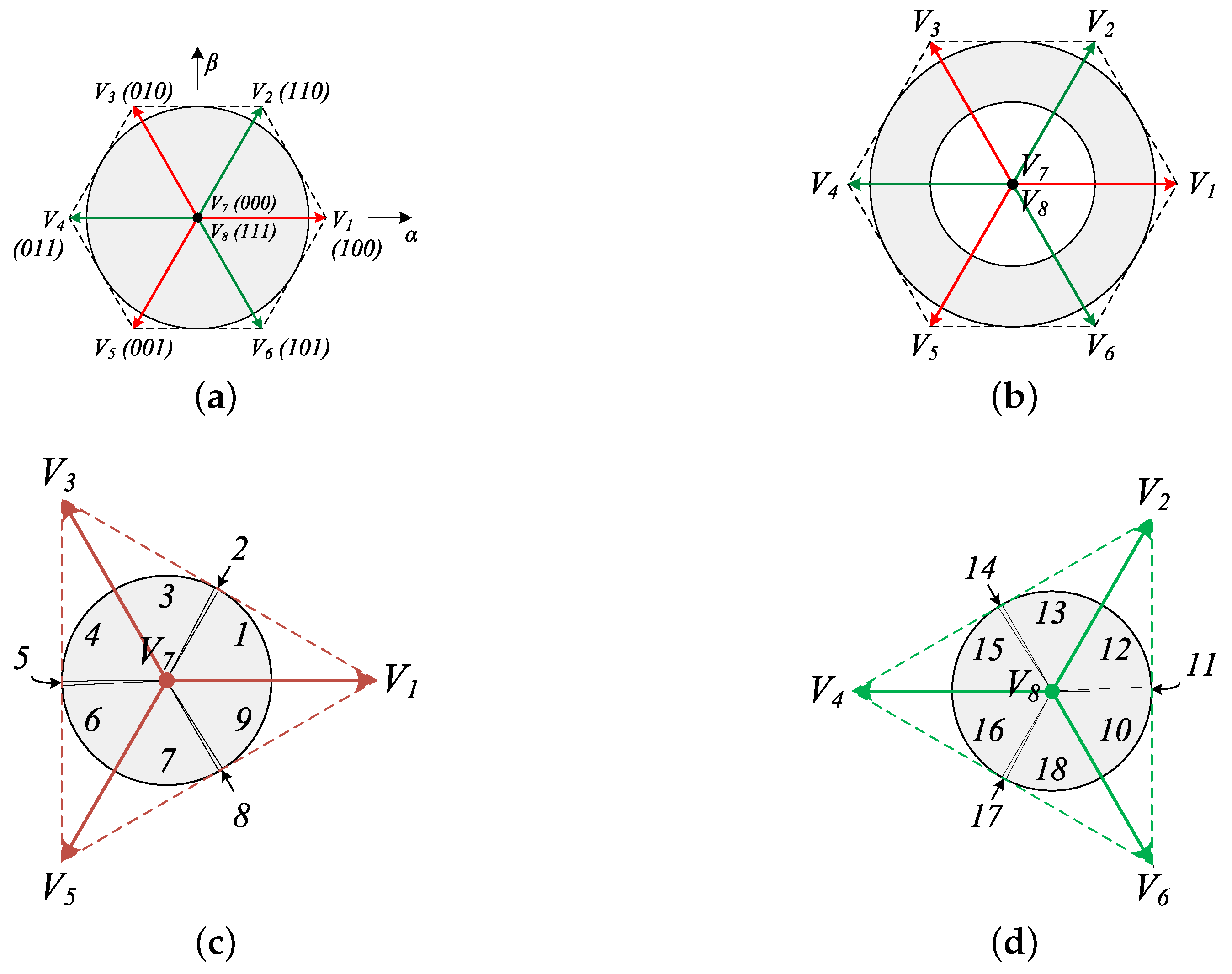
The CCMV SVM adopted for driving the H8 inverter aims to make CMV vary as little as possible. As another mandatory feature, the converter must ensure single-leg commutations, in order for the modulation to be actually feasible.
Figure 7a shows the space vector representation with the corresponding full-bridge configuration in the
plane that will be used in the following analysis. As stated above, the main drawback of this modulation technique is that it applies only to modulation indexes less than 0.5 (shaded areas in
Figure 7c,d). Therefore, a different PWM scheme must be used whenever higher modulation indexes are needed. Traditional SVPWM with DC side decoupling during the inactive states can be adopted in such cases, extending the modulation index range up to
(shaded area in
Figure 7b). SVPWM performs worse than CCMV SVM in terms of CMV; nevertheless, it performs better with the H8 topology than it would if it was used with a conventional three-phase inverter. The two following subsections give a detailed description of the two modulation strategies.
3.3.1. Constant Common-Mode Voltage Space Vector Modulation (CCMV SVM)
CCMV SVM maintains a constant output CMV, using only vectors with the same
.
Table 2 shows the
ratio for the eight SVM states. It is easy to calculate that even active vectors (
,
and
) have
, while odd active vectors (
,
and
) have
. This is true also for the H6, as documented by the thriving literature of optimized modulations that achieve constant common mode voltage [
18] One drawback is that those modulations do not use any inactive vectors (
,
), resulting in more than one bridge leg commutating simultaneously. If the H8 architecture is adopted, thanks to DC decoupling,
values for the inactive vectors are equal to those of the active states, so that it is possible to maintain the CMV constant using all the odd vectors, active and inactive (
,
,
and
), or using the even ones (
,
,
and
). As already mentioned, on each transition from an active vector to an inactive one, the CMV equals
or
, causing a
variation of the CMV.
The reference vector is synthesized in the
plane switching between the two nearest odd or even vectors with the addition of the proper (odd or even) inactive state. The vectors that can be reached using this modulation technique are inside two equilateral triangles with vertices on the used active vectors (
Figure 7c,d). The highest modulation index that can be maintained throughout the full circle is 0.5. SVPWM is used for higher modulation indexes, as described in
Section 3.3.2.
The
plane can be divided into several zones. Considering the odd vectors (
Figure 7c), there are six 60°-wide zones (nr. 1, 3, 4, 6, 7 and 9), plus 3 very narrow slices (zones 2, 5 and 8). The narrow zones are for representing space vector states used for just a single PWM period, and are necessary for having a smooth transition between the two adjacent zones. An equivalent zone partition can be adopted if even vectors are used.
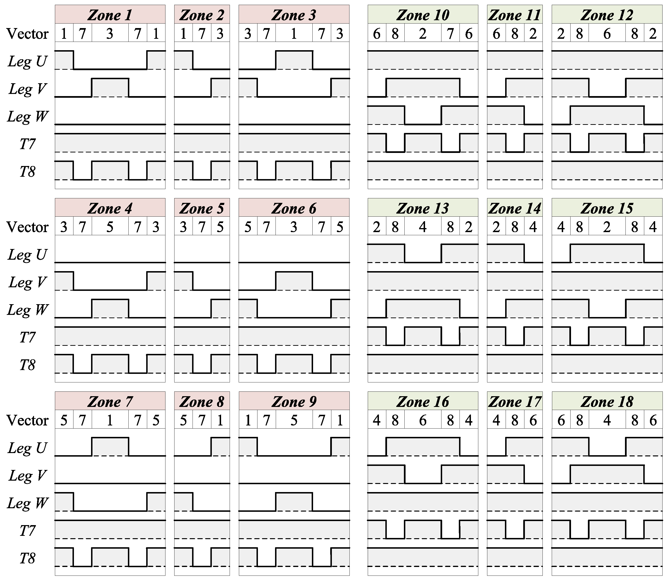
Table 3 reports the vectors used in all the zones for both even and odd vectors CCMV SVM. In order to obtain symmetrical switching periods, one of the two active states in the 60°-wide zones is equally divided in two time slots placed at the beginning and end of each sequence.
Figure 8 shows the output pulse pattern obtained during a switching period for each
plane zone, for even and odd vectors. For the narrow slices (zones 2, 5, 8, 11, 14 and 17), no symmetry is necessary. Moreover, the position of these zones in the
plane means that the modulation values for the two active states will be approximately the same. Since they have only three states instead of five, these intermediate states last half as long as the others, to limit the output current ripple.
3.3.2. Space-Vector Modulation
Considering the voltage limit of the CCMV SVM, when the modulation index exceeds 0.5, an automatic switch to the SVPVM is performed. The duration of inactive vectors during each PWM period is equally divided between
and
; therefore, each sequence has a central symmetry and active states are placed to minimize the switching events with respect to the adjacent inactive states. The DC decoupling switches T7 and T8 are turned off during the zero states. The resulting pulse pattern is shown in
Figure 9, along with the evolution of CMV. It is worth mentioning that this modulation applied to a traditional three-phase converter would exhibit CMV varying from zero to
within each PWM period, whereas the H8 architecture limits the
excursion to
. In comparison to CCMV SVM, more common-mode voltage is present, but still the H8 structure helps to keep its excursion limited.
4. Experimental Results
A prototype of the proposed H8 converter architecture was designed, fabricated and deeply tested. The prototype can be easily converted to H6 topology by disabling T7 and T8 gate drivers and short-circuiting the associated switching devices. In this way H6 SVPWM, H8 SVPWM and H8 CCMV SVM solutions can be implemented and tested using the same prototype, allowing an easy comparison between the three solutions in terms of power quality and efficiency, while a comparison between silicon IGBTs and wide band-gap (SiC) power MOSFETs can be done, simply replacing the switching devices.
The load of the converter was a three phase RL configuration, using a star connection (10 + 2 mH for each phase); while the bus voltage was fixed at 250 V. The prototype uses a PWM frequency of 10 kHz, and produces, at the output, a fundamental frequency of 50 Hz. Although the impedance of the RL load is different from that of an electrical machine, which would have a small resistance and a back electromotive force, this experimental setup can still be used to evaluate the efficiency and common mode voltage performance, since they do not depend on the load but only on the power converter.
4.1. H6 versus H8: Power Quality and Efficiency
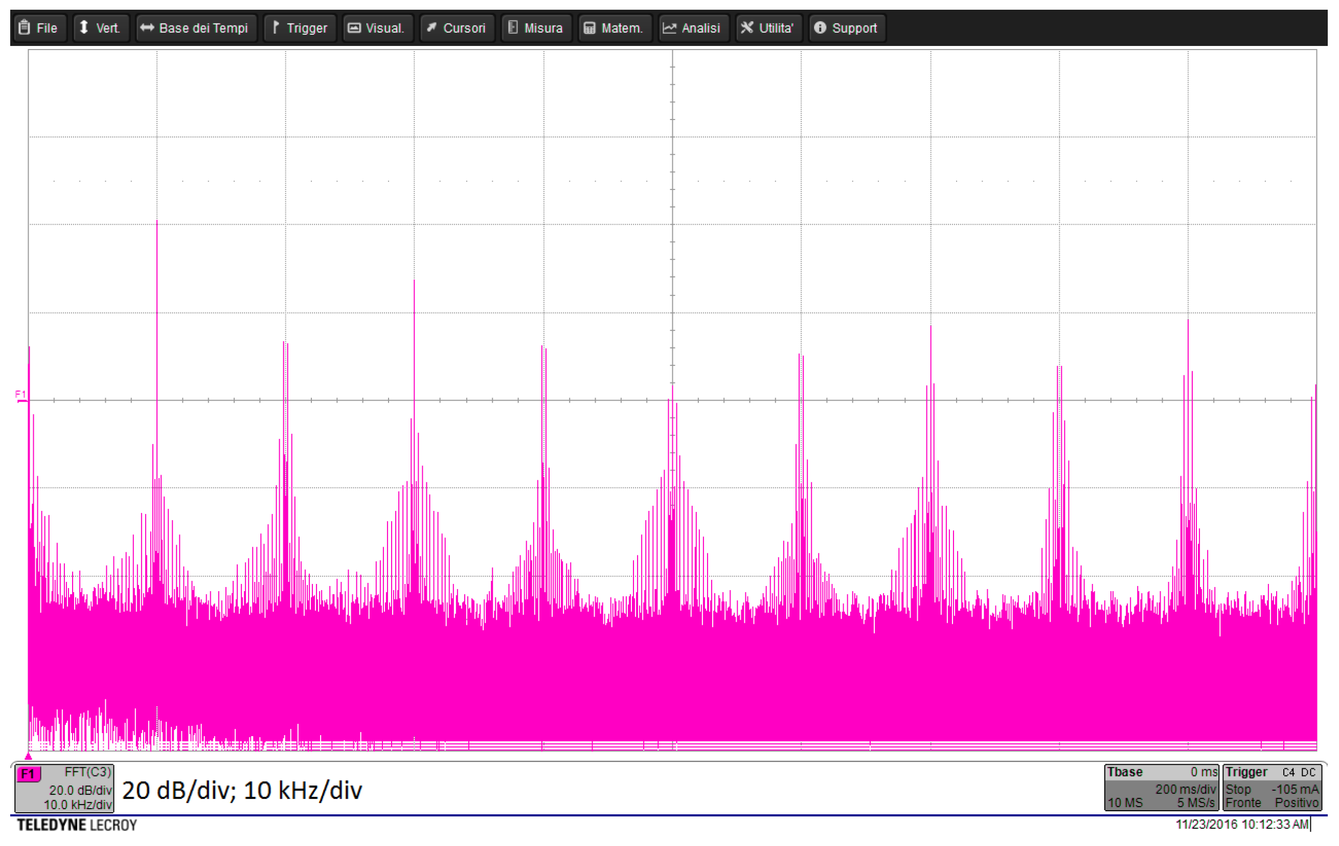
According to [
16], CMV reduction is a key element for both electric drives and photovoltaic applications. As it can be seen from
Figure 10 and
Figure 11, H8 CCMV SVM excels for the
harmonic content. Using the H8 topology and the proposed CCMV SVM, all the harmonics in the spectrum are lower, as summarized in
Table 4.
Regarding the line to line output voltage (
in the following), H6 SVPWM, H8 SVPWM perform in a very similar way as depicted in
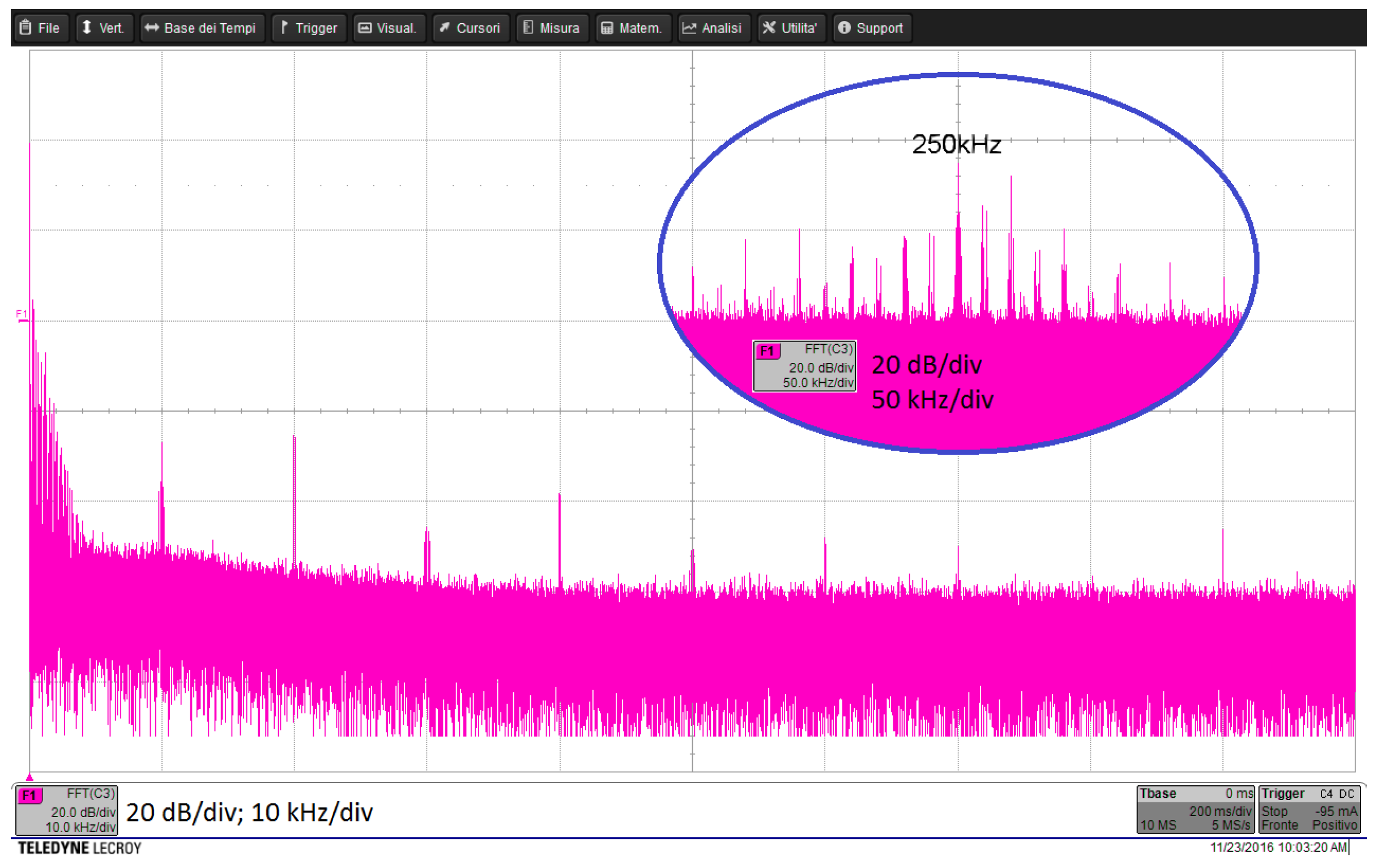
Figure 12, while H8 CCMV SVM shows a similar behavior for all the harmonics components except for the 10 kHz harmonic, that is about 15 dB higher, and a lower spectral components around 250 kHz (as highlighted in the box in
Figure 12).
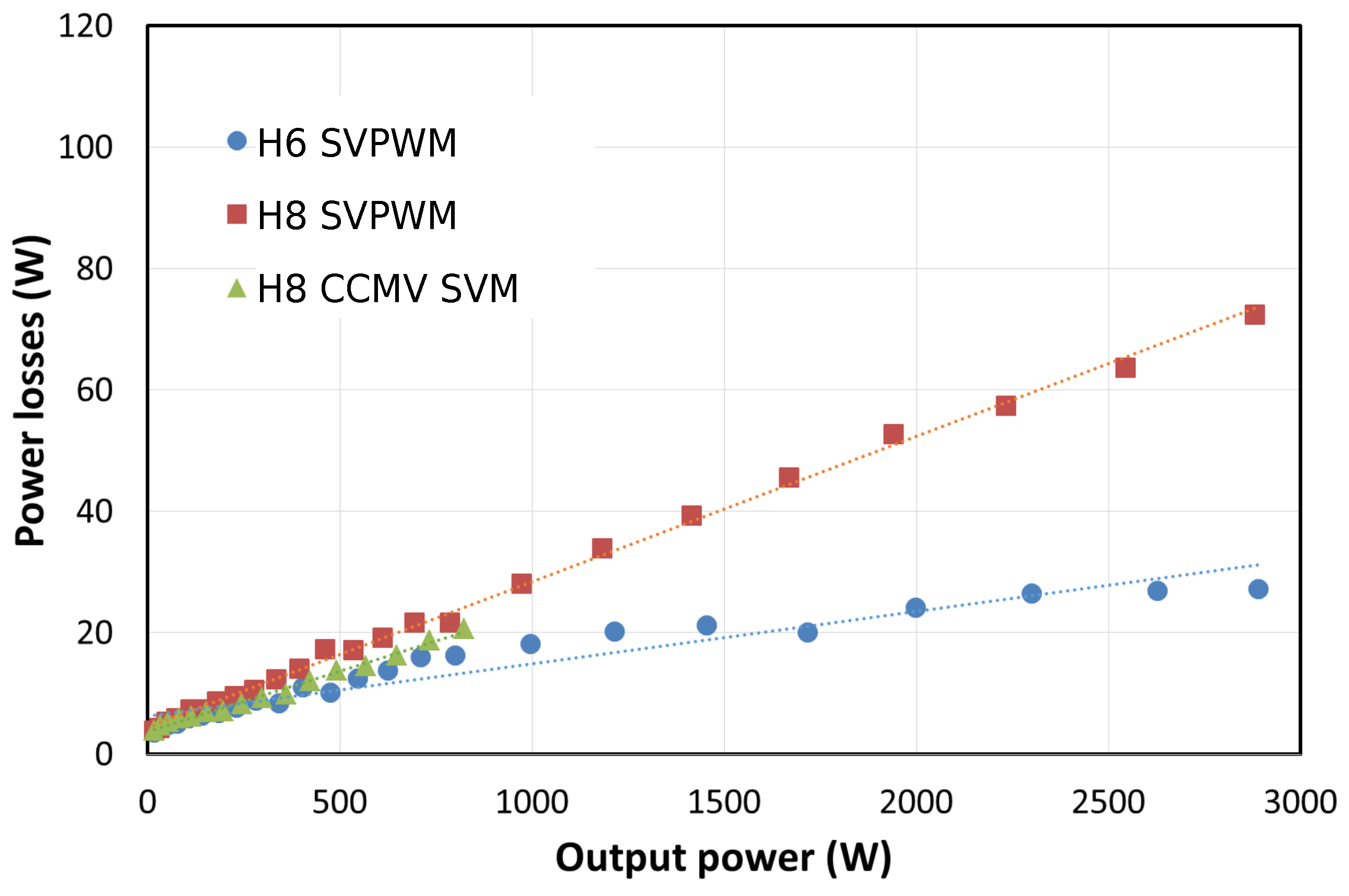
After this comparison in terms of spectral quality, the behavior in terms of efficiency was investigated comparing traditional silicon IGBTs and SiC power MOSFETs. At first the prototype was tested using Infineon IKW50N650H5 IGBTs as switching devices. Efficiency tests were made using H6 SVPWM, H8 SVPWM and H8 CCMV SVM configurations. As expected,
Figure 13 confirms that H6 SVPWM performs better than the other two configurations regardless of the value of the modulation index
m.
H8 CCMV SVM, on the other hand, can work with modulation indexes up to (
), and in this condition it features an efficiency only 0.5% lower than the best in class H6 SVPWM. The losses are 31.2 W for H8 CCMV SVM versus 26.4 W for H6 SVPWM (+18%), as summarized in
Table 5.
Rohm SCT2120AF SiC power MOSFETs, (650 V, 29 A) are then used for the next batch of tests. With a modulation index up to
it is possible to compare the three solutions,
Figure 14 shows the results, while
Table 6 reports some analytical data. Using SiC power MOSFETs, H6 results better than H8.
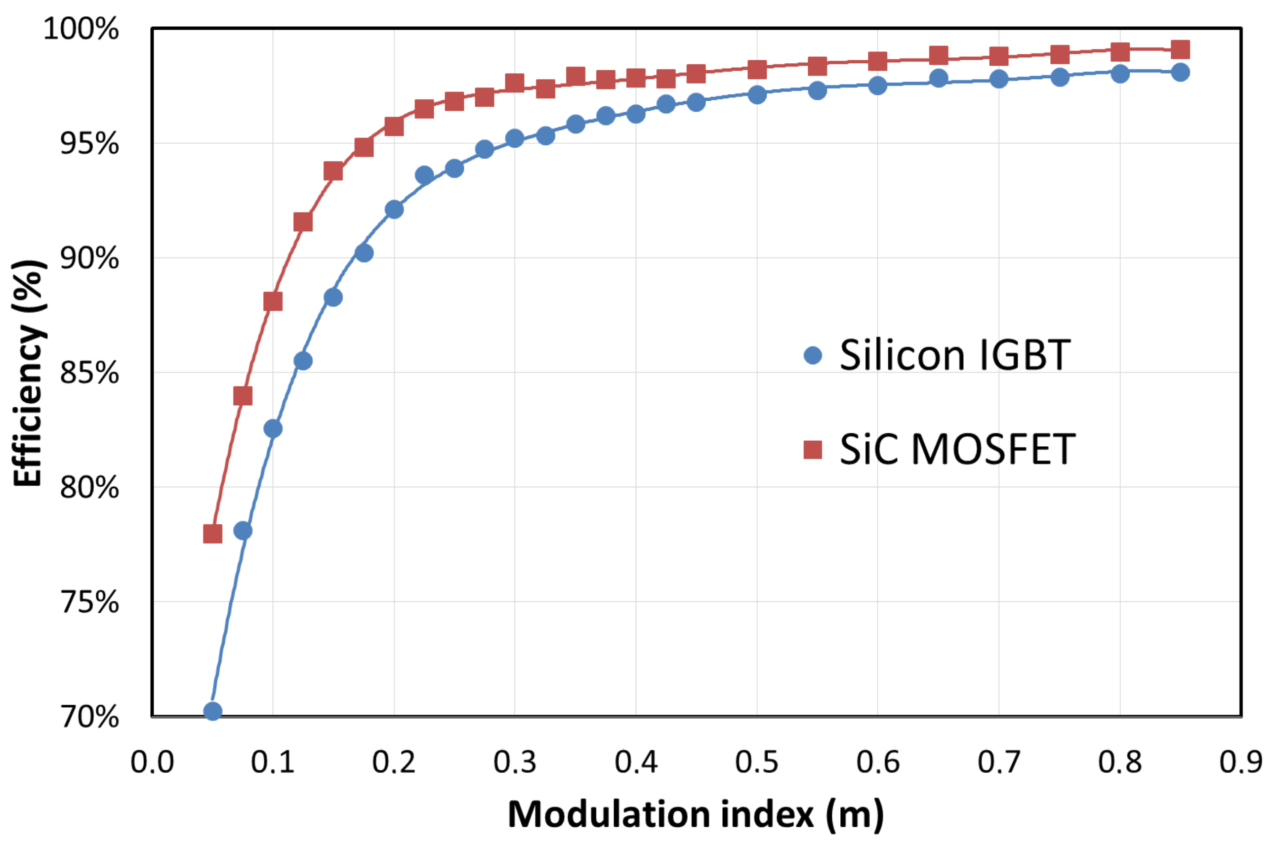
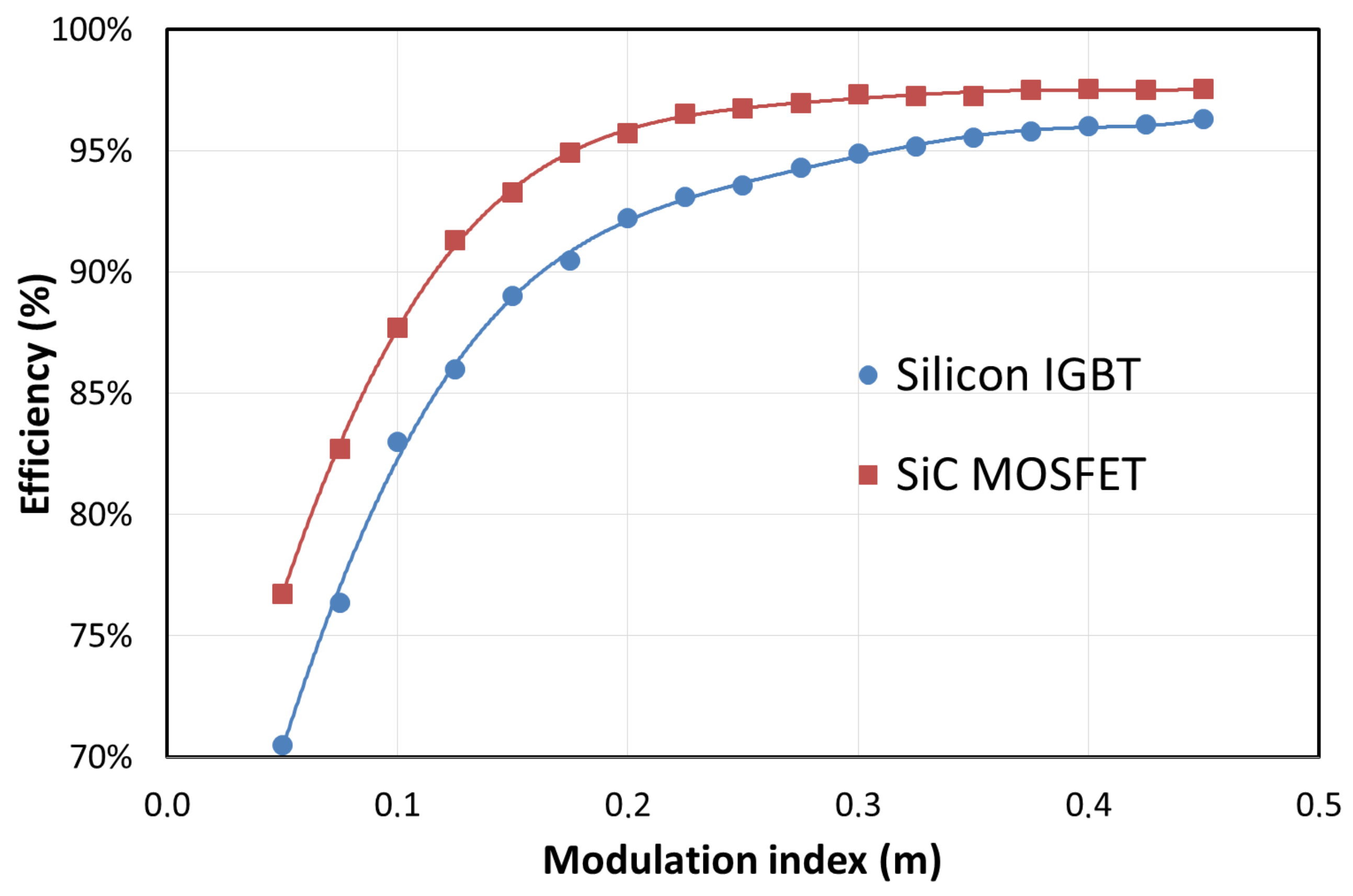
4.2. Performance Comparison
The comparison between Si and SiC two production technologies is a hot research topic. The experiments compare H6 SVPWM, H8 SVPWM and H8 CCMV SVM architectures (
Figure 15 and
Figure 16). SiC devices perform better than the traditional silicon ones for all modulation indexes and for all the proposed architectures. Using H6 SVPWM configuration at high modulation index, the SiC devices efficiency is 0.82% better than using silicon IGBTs, and total power losses are 40% smaller. Having lower losses would allow for a reduced heatsink with a thermal resistance 67% higher. Close to the maximum modulation index for the CCMV SVM (
), a higher efficiency (+0.83%) is achieved by SiC devices.
5. Reliability Study
The efficiency and the power quality of a power electronics converter are only one aspect of the whole system. Although the use of SiC devices does not allow for an improvement in the common-mode voltage generation, the efficiency improvement is unmistakable. However, the SiC semiconductor results in additional cost and efficiency alone is normally not enough to motivate it. An increased efficiency can result in a reduced volume of the heatsink or in the possibility to increase the frequency to reduce the weight of the magnetic components. In the following a different analysis is performed, aiming at quantifying the benefits in terms of lifetime extension of a SiC converter with the same thermal design of an Si one. This question is of industrial interest, because of the possibility to re-use existing thermal designs and the possibility to decrease the maintenance of the products [
21,
22].
The Coffin-Manson-Arrhenius formula is a well-known model to estimate the module’s lifetime given its mission profile [
23] (
2). The number of cycles until failure
is calculated depending on the average operating temperature
and on the amplitude of the thermal cycles
.
is the Boltzmann constant, while coefficients
a,
, and
are usually chosen to fit the equation upon the results of multiple reliability experiments [
24].
As an application example, referring to a motor drive for an electric vehicle, the New European Driving Cycle (NECD) was chosen as a reference; it refers to a specific speed profile as shown at the top of
Figure 17. Several assumptions have been made to match this profile with the devices chosen for this analysis. Considering a maximum electrical frequency of 100 Hz and a peak current amplitude of 15 A, the second plot of
Figure 17 shows the converter’s output power. It is possible, by taking as a reference the datasheet values and an identical thermal design (considering devices packaged in the same power module), to estimate the losses and, consequently, to calculate the resulting junction temperature, as shown for the T1 device at the bottom of
Figure 17 for different semiconductor technologies and modulation. The full-bridge devices experience the most severe losses, because they are always carrying the current, differently from the DC devices.
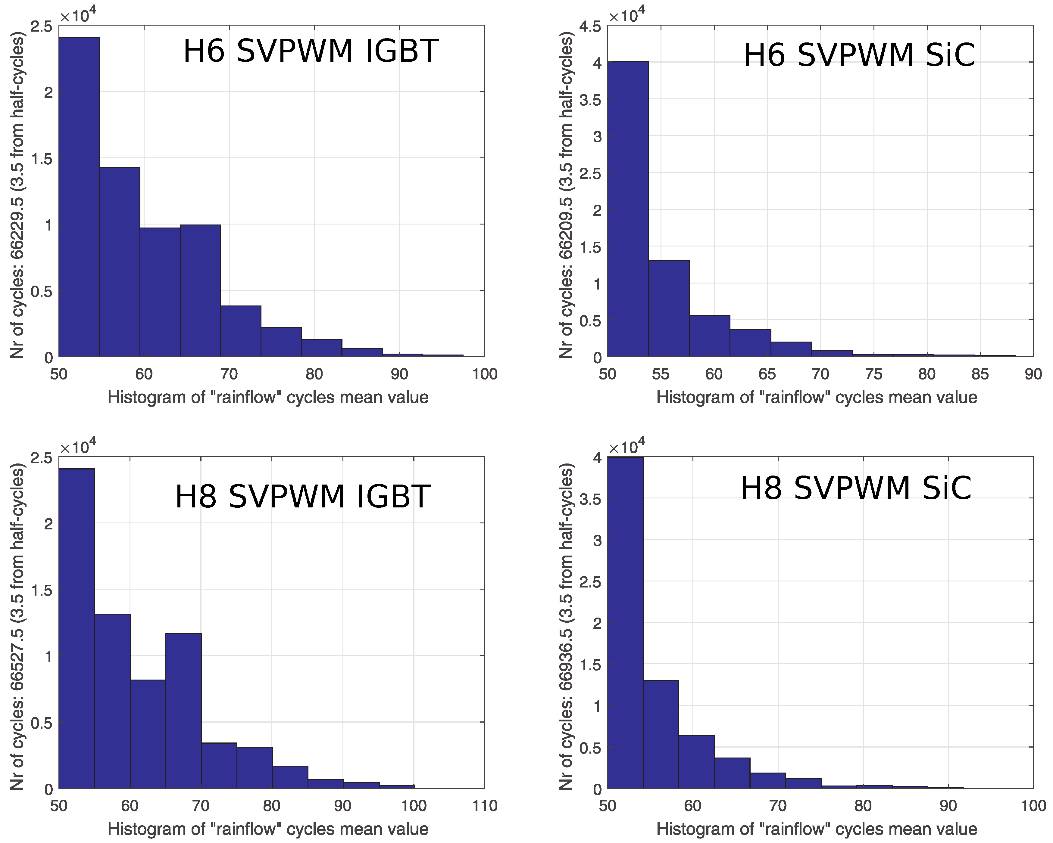
A Rainflow cycle counting procedure is then applied to these profiles, obtaining the graphs of
Figure 18. Considering one hour of average usage per day of the electric car, it is possible to calculate the overall lifetime of the converter by dividing the length of the cycle by the accumulated damage. The results are shown in
Table 7. As can be seen, the lower efficiency of the H8 converter is paid in terms of a reduced lifetime. The reduction is not excessive, because the losses are spread over a greater number of devices, so the lifetime decrease is due to an increase of the case temperature. What is interesting, is that the higher efficiency of SiC devices can reduce the damage due to thermal stress by a factor 4 on average.
Although different failure modes may occur reducing a module lifetime, the above analysis shows that the use of SiC devices, despite higher initial costs, can strongly reduce damage accumulation. The benefits of increased lifetime expectation may justify the additional costs.
6. Conclusions
This paper analyzes the H8 converter applied to the power train of an electrical vehicle. The H8 converter is a modified three-phase bridge with two additional series devices, that decouple the AC load from the power supply during the free-wheeling phase. The main objective is to reduce the common mode voltage, that is a source of electromagnetic interference and decreases the lifetime of the bearings of the electrical machine. Experiments show a marked reduction in the common mode voltage compared to the standard three-phase bridge. A comparison in terms of efficiency and lifetime between SiC and Si transistors is carried out, showing how the SiC solution allows for a marked increase of efficiency and almost four times the lifetime for the same thermal design. This lifetime extension can compensate for the additional cost of the SiC devices compared to the Si ones.
Author Contributions
Conceptualization, D.B and L.C.; methodology, G.B.; software, L.C.; validation, A.T., M.L. and G.F.; formal analysis, L.C.; investigation, M.L.; resources, H.Z.; data curation, C.C.; writing–original draft preparation, G.B.; writing–review and editing, D.B.; visualization, C.C.; supervision, G.F.; project administration, H.Z.; funding acquisition, H.Z.
Funding
This research was funded by Ningbo Science & Technology Bureau under Grants 2017D10031 and 2018A-08-C.
Conflicts of Interest
The authors declare no conflict of interest. The funders had no role in the design of the study; in the collection, analyses, or interpretation of data; in the writing of the manuscript, or in the decision to publish the results’.
References
- Boillat, D.; Kolar, J.; Muehlethaler, J. Volume minimization of the main DM/CM EMI filter stage of a bidirectional three-phase three-level PWM rectifier system. In Proceedings of the 2013 IEEEEnergy Conversion Congress and Exposition (ECCE), Denver, CO, USA, 15–19 September 2013; pp. 2008–2019. [Google Scholar] [CrossRef]
- Gong, X.; Ferreira, J.A. Comparison and Reduction of Conducted EMI in SiC JFET and Si IGBT-Based Motor Drives. IEEE Trans. Power Electron. 2014, 29, 1757–1767. [Google Scholar] [CrossRef]
- Jaeger, C.; Grinbaum, I.; Smajic, J. Numerical simulation and measurement of common-mode and circulating bearing currents. In Proceedings of the 2016 XXII International Conference on Electrical Machines (ICEM), Lausanne, Switzerland, 4–7 September 2016; pp. 486–491. [Google Scholar] [CrossRef]
- Svimonishvili, T.; Fan, F.; See, K.Y.; Liu, X.; Zagrodnik, M.A.; Gupta, A.K. High-frequency model and simulation for the investigation of bearing current in inverter-driven induction machines. In Proceedings of the 2016 IEEE Region 10 Conference (TENCON), Singapore, 22–25 November 2016; pp. 55–59. [Google Scholar] [CrossRef]
- Araújo, R.D.S.; de Rodrigues, R.A.; de Paula, H.; Filho, B.J.C.; Baccarini, L.M.R.; Rocha, A.V. Premature Wear and Recurring Bearing Failures in an Inverter-Driven Induction Motor; Part II: The Proposed Solution. IEEE Trans. Ind. Appl. 2015, 51, 92–100. [Google Scholar] [CrossRef]
- Araújo, R.D.S.; de Paula, H.; de Rodrigues, R.A.; Baccarini, L.M.R.; Rocha, A.V. Premature Wear and Recurring Bearing Failures in an Inverter-Driven Induction Motor; Part I: Investigation of the Problem. IEEE Trans. Ind. Appl. 2015, 51, 4861–4867. [Google Scholar] [CrossRef]
- Piazza, M.C.D.; Luna, M.; Ragusa, A.; Vitale, G. An improved common mode active filter for EMI reduction in vehicular motor drives. In Proceedings of the 2011 IEEE Vehicle Power and Propulsion Conference, Chicago, IL, USA, 6–9 September 2011; pp. 1–8. [Google Scholar] [CrossRef]
- Piazza, M.C.D.; Ragusa, A.; Vitale, G. Effects of Common-Mode Active Filtering in Induction Motor Drives for Electric Vehicles. IEEE Trans. Veh. Technol. 2010, 59, 2664–2673. [Google Scholar] [CrossRef]
- Mutoh, N.; Nakanishi, M.; Kanesaki, M.; Nakashima, J. EMI noise control methods suitable for electric vehicle drive systems. IEEE Trans. Electromagn. Compat. 2005, 47, 930–937. [Google Scholar] [CrossRef]
- Moon, M.; Kim, H.; Song, J.; Kwack, Y.; Kim, D.H.; Kim, B.; Kim, E.; Kim, J. Modeling and analysis of return paths of common mode EMI noise currents from motor drive system in hybrid electric vehicle. In Proceedings of the 2015 Asia-Pacific Symposium on Electromagnetic Compatibility (APEMC), Taipei, Taiwan, 26–29 May 2015; pp. 82–85. [Google Scholar] [CrossRef]
- Kishore, A.; Patki, C.; Anwar, M.; Ivan, W.; Teimor, M. Investigation of common mode noise in electric propulsion system high voltage components in an electrified vehicle. In Proceedings of the 2016 IEEE Transportation Electrification Conference and Expo (ITEC), Dearborn, MI, USA, 27–29 June 2016; pp. 1–6. [Google Scholar] [CrossRef]
- Jeschke, S.; Tsiapenko, S.; Hirsch, H. Investigations on the shaft currents of an electric vehicle traction system in dynamic operation. In Proceedings of the 2015 IEEE International Symposium on Electromagnetic Compatibility (EMC), Dresden, Germany, 16–22 August 2015; pp. 696–701. [Google Scholar] [CrossRef]
- Barater, D.; Concari, C.; Buticchi, G.; Gurpinar, E.; De, D.; Castellazzi, A. Performance Evaluation of a Three-Level ANPC Photovoltaic GridConnected Inverter With 650-V SiC Devices and Optimized PWM. IEEE Trans. Ind. Appl. 2016, 52, 2475–2485. [Google Scholar] [CrossRef]
- Gurpinar, E.; Yang, Y.; Iannuzzo, F.; Castellazzi, A.; Blaabjerg, F. Reliability-Driven Assessment of GaN HEMTs and Si IGBTs in 3LANPC PV Inverters. IEEE J. Emerg. Sel. Top. Power Electron. 2016, 4, 956–969. [Google Scholar] [CrossRef]
- Han, D.; Morris, C.T.; Lee, W.; Sarlioglu, B. A Case Study on Common Mode Electromagnetic Interference Characteristics of GaN HEMT and Si MOSFET Power Converters for EV/HEVs. IEEE Trans. Transp. Electr. 2017, 3, 168–179. [Google Scholar] [CrossRef]
- Concari, L.; Barater, D.; Buticchi, G.; Concari, C.; Liserre, M. H8 Inverter for Common-Mode Voltage reduction in Electric Drives. IEEE Trans. Ind. Appl. 2016, 52, 4010–4019. [Google Scholar] [CrossRef]
- Concari, L.; Barater, D.; Concari, C.; Toscani, A.; Buticchi, G.; Liserre, M. H8 architecture for reduced common-mode voltage three-phase PV converters with silicon and SiC power switches. In Proceedings of the IECON 2017—43rd Annual Conference of the IEEE Industrial Electronics Society, Beijing, China, 29 October–1 November 2017; pp. 4227–4232. [Google Scholar] [CrossRef]
- Hava, A.; Un, E. A High-Performance PWM Algorithm for Common-Mode Voltage Reduction in Three-Phase Voltage Source Inverters. IEEE Trans. Ind. Electron. 2011, 26, 1998–2008. [Google Scholar] [CrossRef]
- Hava, A.; Un, E. Performance Analysis of Reduced Common-Mode Voltage PWM Methods and Comparison With Standard PWM Methods for Three-Phase Voltage-Source Inverters. IEEE Trans. Power Electron. 2009, 24, 241–252. [Google Scholar] [CrossRef]
- Li, K.; Lu, T.; Zhao, Z.; Yin, L.; Liu, F.; Yuan, L. Carrier based implementation of reduced common mode voltage PWM strategies. In Proceedings of the 2013 IEEE ECCE Asia Downunder (ECCE Asia), Melbourne, VIC, Australia, 3–6 June 2013; pp. 578–584. [Google Scholar] [CrossRef]
- Yang, S.; Bryant, A.; Mawby, P.; Xiang, D.; Ran, L.; Tavner, P. An Industry-Based Survey of Reliability in Power Electronic Converters. IEEE Trans. Ind. Appl. 2011, 47, 1441–1451. [Google Scholar] [CrossRef]
- Colmenares, J.; Sadik, D.P.; Hilber, P.; Nee, H.P. Reliability analysis of a high-efficiency SiC three-phase inverter for motor drive applications. In Proceedings of the 2016 IEEE Applied Power Electronics Conference and Exposition (APEC), Long Beach, CA, USA, 20–24 March 2016; pp. 746–753. [Google Scholar] [CrossRef]
- Blaabjerg, F.; Ma, K.; Zhou, D. Power electronics and reliability in renewable energy systems. In Proceedings of the IEEE International Symposium on Industrial Electronics (ISIE), Hangzhou, China, 28–31 May 2012; pp. 19–30. [Google Scholar]
- Wintrich, A.; Nicolai, U.; Tursky, W.; Reimann, T. Semikron, Application Manual Power Semiconductors. Available online: https://www.semikron.com/service-support/application-manual.html (accessed on 1 May 2019).
Figure 1.
Common-mode current path in an electrical drive system.
Figure 1.
Common-mode current path in an electrical drive system.
Figure 2.
Block scheme of the control for a three-phase motor drive inverter.
Figure 2.
Block scheme of the control for a three-phase motor drive inverter.
Figure 3.
Definition of A- and B-regions on the space vector (SV) diagram.
Figure 3.
Definition of A- and B-regions on the space vector (SV) diagram.
Figure 4.
Reference voltage formation for the RCMV-PWM. Shaded areas indicate the regions where the depicted sets of vectors are employed.
Figure 4.
Reference voltage formation for the RCMV-PWM. Shaded areas indicate the regions where the depicted sets of vectors are employed.
Figure 6.
DC side of the H8 inverter: voltage divider (a) and decoupling network (b).
Figure 6.
DC side of the H8 inverter: voltage divider (a) and decoupling network (b).
Figure 7.
plane space vector diagrams. Odd vectors (red), even vectors (green). (a) SV vectors. (b) Modulation index region where SVPWM is used . (c) Feasability region and modulation zone numbers for odd CCMV SVM. (d) Feasability region and modulation zone numbers for even CCMV SVM.
Figure 7.
plane space vector diagrams. Odd vectors (red), even vectors (green). (a) SV vectors. (b) Modulation index region where SVPWM is used . (c) Feasability region and modulation zone numbers for odd CCMV SVM. (d) Feasability region and modulation zone numbers for even CCMV SVM.
Figure 8.
State sequences for CCMV SVM in H8 converter. Zones from 1 to 9 employ odd vectors, zones from 10 to 18 even ones.
Figure 8.
State sequences for CCMV SVM in H8 converter. Zones from 1 to 9 employ odd vectors, zones from 10 to 18 even ones.
Figure 9.
Vectors usage and switch pulse pattern throughout the rotational period for the SVPWM. Only one PWM period is presented. Red represents the odd vectors, whereas green the even ones.
Figure 9.
Vectors usage and switch pulse pattern throughout the rotational period for the SVPWM. Only one PWM period is presented. Red represents the odd vectors, whereas green the even ones.
Figure 10.
CMV spectrum; H6 architecture and SVPWM. Modulation index m = 0.4. Frequency range of 0–100 kHz.
Figure 10.
CMV spectrum; H6 architecture and SVPWM. Modulation index m = 0.4. Frequency range of 0–100 kHz.
Figure 11.
CMV spectrum; H8 architecture and CMMV SVM. Modulation index m = 0.4. Frequency range of 0–100 kHz.
Figure 11.
CMV spectrum; H8 architecture and CMMV SVM. Modulation index m = 0.4. Frequency range of 0–100 kHz.
Figure 12.
Spectral analysis of the voltage output of H6 converter. Frequency range of 0–100 kHz in the main figure, 200–300 kHz in the small round box [
17].
Figure 12.
Spectral analysis of the voltage output of H6 converter. Frequency range of 0–100 kHz in the main figure, 200–300 kHz in the small round box [
17].
Figure 13.
Power losses of silicon IGBTs versus output power [
17].
Figure 13.
Power losses of silicon IGBTs versus output power [
17].
Figure 14.
Power losses of SiC power MOSFETs versus output power [
17].
Figure 14.
Power losses of SiC power MOSFETs versus output power [
17].
Figure 15.
Efficiency comparison with different semiconductors: H6 SVPWM architecture [
17].
Figure 15.
Efficiency comparison with different semiconductors: H6 SVPWM architecture [
17].
Figure 16.
Efficiency comparison with different semiconductors: H8 CCMV SVM architecture [
17].
Figure 16.
Efficiency comparison with different semiconductors: H8 CCMV SVM architecture [
17].
Figure 17.
Junction temperature evaluation with silicon IGBTs and SiC power MOSFETs according to the New European Driving Cycle.
Figure 17.
Junction temperature evaluation with silicon IGBTs and SiC power MOSFETs according to the New European Driving Cycle.
Figure 18.
Accumulated damage at different average junction temperatures.
Figure 18.
Accumulated damage at different average junction temperatures.
Table 1.
Vector patterns for various space-vector methods.
Table 1.
Vector patterns for various space-vector methods.
| SV Method | A1 | A2 | A3 | A4 | A5 | A6 |
| SVPWM | 7210127 | 7230327 | 7430347 | 7450547 | 7650567 | 7610167 |
| AZSPWM1 | 3216123 | 4321234 | 5432345 | 6543456 | 1654561 | 2165612 |
| AZSPWM2 | 6213126 | 1324231 | 2435342 | 3546453 | 4651564 | 5162615 |
| AZSPWM3 | 12421 | 23532 | 34643 | 45154 | 56265 | 61316 |
| RSPWM1 | 31513 | 31513 | 31513 | 31513 | 31513 | 31513 |
| RSPWM2A | 31513 | 13531 | 13531 | 15351 | 15351 | 31513 |
| RSPWM2B | 42624 | 42624 | 24642 | 24642 | 26462 | 26462 |
| | B1 | B2 | B3 | B4 | B5 | B6 |
| RSPWM3 | 31513 | 42624 | 13531 | 24642 | 15351 | 26462 |
| NSPWM | 21612 | 32123 | 43234 | 54345 | 65456 | 16561 |
| | B1 | A1 | B2 | A2 | B3 | A3 | B4 | A4 | B5 | A5 | B6 | A6 | B1 |
| DPWM1 | 72127 | 23032 | 74347 | 45054 | 76567 | 61016 | |
| | 21012 | 72327 | 43034 | 74547 | 65056 | 76167 |
| DPWM2 | 72127 | 23732 | 74347 | 45754 | 76567 | 61716 | |
| | 21712 | 72327 | 43734 | 74547 | 65756 | 76167 |
Table 2.
Common-mode voltage () values.
Table 2.
Common-mode voltage () values.
| | Vector | | | | |
|---|
| H6 | H8 |
|---|
| | | 1 | 0 | 0 | | |
| | | 1 | 1 | 0 | | |
| | | 0 | 1 | 0 | | |
| | | 0 | 1 | 1 | | |
| | | 0 | 0 | 1 | | |
| | | 1 | 0 | 1 | | |
| H6 | | 0 | 0 | 0 | 0 | |
| 1 | 1 | 1 | 1 | |
| H8 | | | | | | |
| | | | | |
Table 3.
Vectors used in the CCMV SVM strategy.
Table 3.
Vectors used in the CCMV SVM strategy.
| Angles | Odd Vectors | Even Vectors |
|---|
| 0°–60° | | |
| 60°–120° | |
| 120°–180° | | |
| 180°–240° | |
| 240°–300° | | |
| 300°–360° | |
Table 4.
Harmonic content comparison between H8 CCMV SVM and H6 SVPWM.
Table 4.
Harmonic content comparison between H8 CCMV SVM and H6 SVPWM.
| Harmonic | Reduction H8 CCMV SVM vs. H6 SVPWM [dB] |
|---|
| 1st | −28 |
| 2nd | 0 |
| 3rd | −28 |
| 4th | −4 |
| 5th | −8 |
| 6th | −16 |
| 7th | −16 |
Table 5.
Comparison between H6 SVPWM, H8 SVPWM and H8 CCMV SVM with Silicon IGBT.
Table 5.
Comparison between H6 SVPWM, H8 SVPWM and H8 CCMV SVM with Silicon IGBT.
| Architecture | | |
|---|
| | (%) | (W) | (%) | (W) |
|---|
| H6 SVPWM | 96.8 | 26.4 | 98.1 | 55 |
| H8 SVPWM | 95.1 | 39.7 | 95.5 | 102 |
| H8 CCMV SVM | 96.3 | 31.2 | n.a. | n.a. |
Table 6.
Efficiency and total power loss comparison among H6 SVPWM, H8 SVPWM and H8 CCMV SVM. SiC power MOSFETs switching devices [
17].
Table 6.
Efficiency and total power loss comparison among H6 SVPWM, H8 SVPWM and H8 CCMV SVM. SiC power MOSFETs switching devices [
17].
| Architecture | | |
|---|
| | (%) | (W) | (%) | (W) |
|---|
| H6 SVPWM | 97.7 | 19.2 | 98.9 | 32.6 |
| H8 SVPWM | 96.9 | 25.5 | 97.1 | 85.6 |
| H8 CCMV SVM | 97.1 | 24.3 | n.a. | n.a. |
Table 7.
Expected lifetime forecast through rainflow analysis.
Table 7.
Expected lifetime forecast through rainflow analysis.
| Case Study | Lifetime (Years) |
|---|
| H6 SVPWM IGBT | 16.6 |
| H6 SVPWM SiC | 67.7 |
| H8 SVPWM IGBT | 13.2 |
| H8 SVPWM SiC | 54.9 |
© 2019 by the authors. Licensee MDPI, Basel, Switzerland. This article is an open access article distributed under the terms and conditions of the Creative Commons Attribution (CC BY) license (http://creativecommons.org/licenses/by/4.0/).

 ,
, 


