Article

Switched-Capacitor Boost Converter for Low Power Energy Harvesting Applications

Faculty of Electrical Engineering and Computer Science, University of Maribor, Koroška Cesta 46, SI-2000 Maribor, Slovenia
*
Author to whom correspondence should be addressed.
Energies 2018, 11(11), 3156; https://doi.org/10.3390/en11113156
Submission received: 19 October 2018 / Revised: 8 November 2018 / Accepted: 13 November 2018 / Published: 14 November 2018
(This article belongs to the Section F: Electrical Engineering)

Abstract

:
The paper presents a Switched-Capacitor Boost DC-DC Converter (SC-BC) which can be used in energy harvesting applications using thermoelectric generators (TEGs) with low output voltage, low power and a significant internal resistance. It consists of a switching capacitor circuit, where MOSFETs are used as switches, and a boost stage. The converter is a modification of a previously presented scheme in which diodes are used in the switched capacitor stage. A higher voltage gain and an increased efficiency can thus be achieved. The model of the converter was developed considering the internal resistance of the TEG and boost stage inductor. A comparison with the diode based converter is shown, with consideration of the TEG internal resistance. Calculation is presented of the main passive components. A control algorithm is also proposed and evaluated. It is based on a linearization approach, and designed for output voltage and inductor current control. The operation of both converter and control are verified with the simulation and experimental results.

1. Introduction

Photovoltaic (PV) systems suffer from temperature-related reduction of the produced power in the case of increased temperature of the panel surface. The current state-of-art in this field is to use passive cooling with a liquid coolant [1,2], but researchers have also focused on radiative cooling approaches [3,4]. An idea for the solution of this problem is to apply thermoelectric generators (TEGs) to the back of the panels and, thus, provide active cooling [5,6]. Furthermore, because the TEGs also produce energy due to the temperature difference between their surfaces, this effect can be used for cogeneration purposes, as energy harvesting [7,8]. Theamount of energy produced is relatively low when compared to that produced by the PV panels, but it is sufficient to allow an increase of the PV panel power production. The main problem when using low temperature TEGs is their low output voltage (a few volts), therefore, an appropriate DC-DC converter has to be used. In such a converter, all the applied diodes represent a significant voltage drop. Also, the TEG itself has a significant internal resistance (in the range of Ohms). These facts stimulated the researchers in the field to investigate different inverter structures with high voltage gains [9,10,11].
The classical solution would be to use a Continuous Conduction Mode or Discontinuous Conduction Mode (CCM/DCM) boundary operated boost converter, with few switching elements and, therefore, high efficiency and low losses [12]. The limitations of this structure occur due to the high internal resistance of the TEG, which limits the voltage gain of the converter. Additionally, when high voltage gain is required, the converter has to operate with either very low or very high duty cycles (down to 0.1 or up to 0.9), resulting in reduced efficiency and, in some cases, highly nonlinear behaviour. Another option would be to use the Luo-superlift converter [13,14]. However, the limitations of this converter are also in the voltage gain limitations. Namely, to achieve a voltage gain in the range of 10 or higher, multiple stages would be required in the converter, which would result in a higher number of switching elements and decreased efficiency.
The use of transformers in the converter, as it is in the case with a flyback converter, would be another option [13]. With the appropriate transformer applied, high voltage gain could be achieved easily. The problem of using such converter would be due to the power dissipation on the leakage inductance of the transformer. Moreover, if the converter application does not require isolation, the cost, losses, mass and volume of the converter would increase significantly. Other candidates, switched-capacitor converters [15,16], operate with relatively low efficiency and introduce di/dt related problems into the circuit. Intuitively, putting two or more converters into cascade could also be an option. However, the losses of converters would add up, resulting in reduced efficiency of the system. So-called quadratic converters [17,18,19,20] can achieve the voltage gain of the cascaded converters with fewer switches, but voltage or current overstresses could be present. Finally, hybrid converters are becoming an interesting solution [21,22,23,24,25]. An interesting approach, combining switching-capacitor and boost converter, was presented in [26,27] (Figure 1). The converter is capable of achieving high voltage gain (in the range of 10). However, the problem with this converter is that a high number of diodes is applied, each of them introducing a significant voltage drop and, thus, a new structure replacing the diodes with the MOSFET transistors is proposed in this paper. The voltage gain of the converter is increased significantly when compared to the converter using diodes. The efficiency is improved, because the voltage drop on the transistors is smaller than the one on the diodes, and, in the switched capacitor circuit, the voltage drop in a diode based converter is on two diodes and one MOSFET, whereas in a MOSFET based converter, the voltage drop is on two MOSFETs. The same is true for the power losses. The improvements regarding the gain characteristics are demonstrated using analytical methods and experimental results in the form of the measurements` results. The modelling was done using a realistic TEG source model, where the internal resistance is significant. This means that the voltage drops on MOSFETs can be neglected, or presented as a part of the internal resistance of the source. Likewise, capacitors have a very small ESR (Equivalent Series Resistance), so it is much lower than the resistance of the TEG and load, and can be neglected. A control algorithm is proposed and evaluated. The linearization method was used, as presented in [28,29]. The model was first linearised, and afterwards controlled with the linear controller.
The research focuses regarding the use of power electronics converters in the applications of energy harvesting are in the solving of problems of using the low power and output voltage devices (like TEGs) more efficiently with either a reduced number of elements, or by integration in dedicated Systems on Chip (SOC). Due to their high cost, volume and weight, the goal is to reduce the number of inductors, as well as their inductance, or to replace them with capacitors. In many cases, diodes are used as passive switching elements, which introduce a significant voltage drop into the circuit, resulting in significant conducting power losses. The problems connected with the high internal resistance of TEG are also addressed. In the field of development of DC-DC converters in such applications, the increasing of voltage gain and efficiency are the main issues, because limits are set to them based on the converter setup and elements. For example, in several converter topologies the duty cycle can become very low or very high in the case when a high voltage gain is required. This can result in highly nonlinear, or even unstable, behaviour. The focus is also on the possibility of using lower voltage and current switches, as well as reducing the overall element count.
The main contributions of this paper are the improvement of an existing DC-DC converter scheme presented in [26,27], modelling of the converter, the derivation of the algorithm for choice of passive components, and the design of the model-based nonlinear control algorithm. The improvement of the converter is achieved by the replacement of the passive switching elements (diodes) with the active ones (MOSFETs), thereby reducing conduction losses significantly, which is represented in improved efficiency (95% at the maximum point compared to 79% in the case of the diode based converter). Additionally, the duty cycle is not overlong or overshort. The model of the converter was obtained using the state space averaging method, as presented in [30]. The model is used for the evaluation of static behaviour (voltage gain), choice of parameters for the passive elements (inductors and capacitors), and design of the control algorithms. Internal resistance of TEG is taken into account in the modelling of the system. The design and control are evaluated with simulations and experiments.
The paper is organised as follows: Section 1 gives an introduction of the PV system upgraded with the introduction of TEG for thermal energy harvesting. The need for the use of a high voltage gain DC-DC converter is presented, based on the problems occurring with the use of TEG. Several existing solutions are presented briefly, and a new Switched-Capacitor Boost DC-DC Converter (SC-BC) structure is introduced. The principle of the operation for this new structure is described in detail in Section 2, where modes of the operation are described. In Section 3, the modelling of SC-BC is presented. A state-space model was developed using the state averaging principle. The resulting dynamic model is represented with formulas and a block scheme. The gain characteristics of the converter are presented in Section 4. Choice of the SC-BC passive components is described in Section 5. The derivation and explanation of the control algorithm for SC-BC is done in Section 6. A model-based approach was used, applying the linearization principle. Results are presented in Section 7, where the verification of static characteristics and control algorithm with the simulation and experimental results are given. In Section 8, a discussion is presented regarding the results and findings.

2. Principle of Operation

Figure 1 shows the Switching-Capacitor-Boost Converter (SC-BC) introduced in [15]. The hybrid converter consists of two stages. The first stage is a Switching-Capacitor circuit (SC, red frame in Figure 1), which is responsible for multiplying the input voltage by the parallel-series interconnecting operation, and the second stage is the Boost Stage (BS, blue frame in Figure 1), further increasing the output voltage. In this scheme, the voltage source is supposed to be ideal. However, when it is applied for energy harvesting using TEG as an input, this voltage source has a significant inner resistance Rg (in the range of 1 Ω to 3 Ω). The diode voltage drops also result in significant reduction of the total converter voltage gain. The detailed scheme of this converter is shown in Figure 2a, where the internal resistance Rg is considered, and MOSFETs are applied as switches S1 to S5.
To reduce the voltage drop in the switching capacitor stage, the improved structure of SC-BC, where the diodes are replaced by MOSFETs, is presented in Figure 2b. The SC-BC operates in three modes. For the diode variant in the first sequence the switches T4 and T5 are switched on and T1, T2, and T3 are switched off. The capacitors C1, C2 and C3 are charged, and also the inductor current iL starts charging the inductor L. The slope of inductor current is defined by converter input voltage vgg (vg is the open terminal TEG voltage) and inductance L. The voltages vC1, vC2 and vC3 on the SC stage capacitors are rising. Capacitor voltage v0 is discharged to the load R0. iR0 is the output load current.
An equivalent circuit for this mode of operation is shown in Figure 3a. Voltage drops on diodes are represented by VD. The same mode of operation is shown in Figure 3b for a MOSFET based converter, where the transistors T1d, T2d, T3d, T4d, T5d, and T6d, as well as switch T4, are switched on, whereas the transistors T1, T2, and T3 are switched off. In the second sequence for the diode circuit, T5 is switched off and transistors T1, T2, T3 and T4 are switched on, and, for the MOSFET circuit, transistors T1d, T2d, T3d, T4d, T5d, and T6d are switched off, whereas the transistors T1, T2, T3, and T4 are switched on. The equivalent circuit is equal for diode and MOSFET based converters, and is shown in Figure 3c. In this mode, the voltages vgg, vC1, vC2 and vC3 are series connected and provide the higher voltage to the BS input, charging the inductor L with their sum. The slope of the inductor current increased as a consequence of higher input voltage in the boost converter stage. Capacitor voltage v0 is, as in the first sequence, discharged to the load R0. In the third sequence, transistors T1, T2 and T3 are switched on in both converters, whereas the transistors T4 and T5 are switched off in the diode-based circuit, and the transistors T4, T1d, T2d, T3d, T4d, T5d, and T6d are switched off in the MOSFET based circuit. The energy stored in inductor L, combined with the voltage source and the energy stored in capacitors C1, C2 and C3, is pushed into the output capacitor C0 and supports the output voltage v0, at the same time, charging the load R0.
An equivalent circuit for this mode of operation is shown in Figure 3d and is, as in the case of the second sequence, equal for diode and MOSFET based converters. The transistors in the circuit are represented by their resistances: rds1 for T1, rds2 for T2, rds3 for T3, rds4 for T4, rds5 for T5, rd1 for T1d, rd2 for T2d, rd3 for T3d, rd4 for T4d, rd5 for T5d, and rd6 for T6d. The same transistors are used for all of the switches; therefore, all the resistances are the same. The resistance of inductor L is represented by the resistance RL.
Figure 4a,b shows the corresponding triggering signals, inductor current and voltage vL in the SC-BC for diode and MOSFET based structures, respectively. The duration of the first sequence is zdTs, where z is the switched capacitors’ charging duty cycle over the interval dTs, where d is the duty cycle function over the interval Ts (Ts = 1/fs, where fs is the switching frequency of the converter). The duration of the second sequence is (1 − z) dTs, and the duration of the third sequence is (1 − d) Ts. The average values of z and d are represented with Z and D, respectively, and the average value of the inductor current iL is represented by IL.

3. SC-BC Modelling

The state space averaging method was used in order to obtain the dynamic model and static characteristics of both converter structures. The Schottky diodes (VSSB420S-M3 with forward voltage VD = 0.8 V) were chosen in the case of diode based converters. The voltage drop on the diode was significant compared to the one expected on the MOSFET on-resistance (RDS(on) = 10 mΩ), indicated in the Figure 3a–d by rd1rd6, rds1rds5. The voltage drop on the RDS(on) (MOSFET drain-source on resistance) was evaluated as 2.5% of the voltage drop on the diodes and can be neglected, as well as the equivalent series resistances of capacitors. Equal values are used for capacitances of capacitors C1, C2 and C3:
C 1 = C 2 = C 3 = C k ,
and, for both converters, it can be assumed that the three legs of the switched capacitor circuit are symmetrical, resulting in:
v C 1 = v C 2 = v C 3 = v C k
Voltages vC1, vC2, and vC3 are, thus, replaced by the voltage vCk in the following text. In order to perform mathematical analysis of SC-BC for static analyses (gain calculation) and controller parameter design, the dynamic model needs to be derived for diode and MOSFET-based converters.

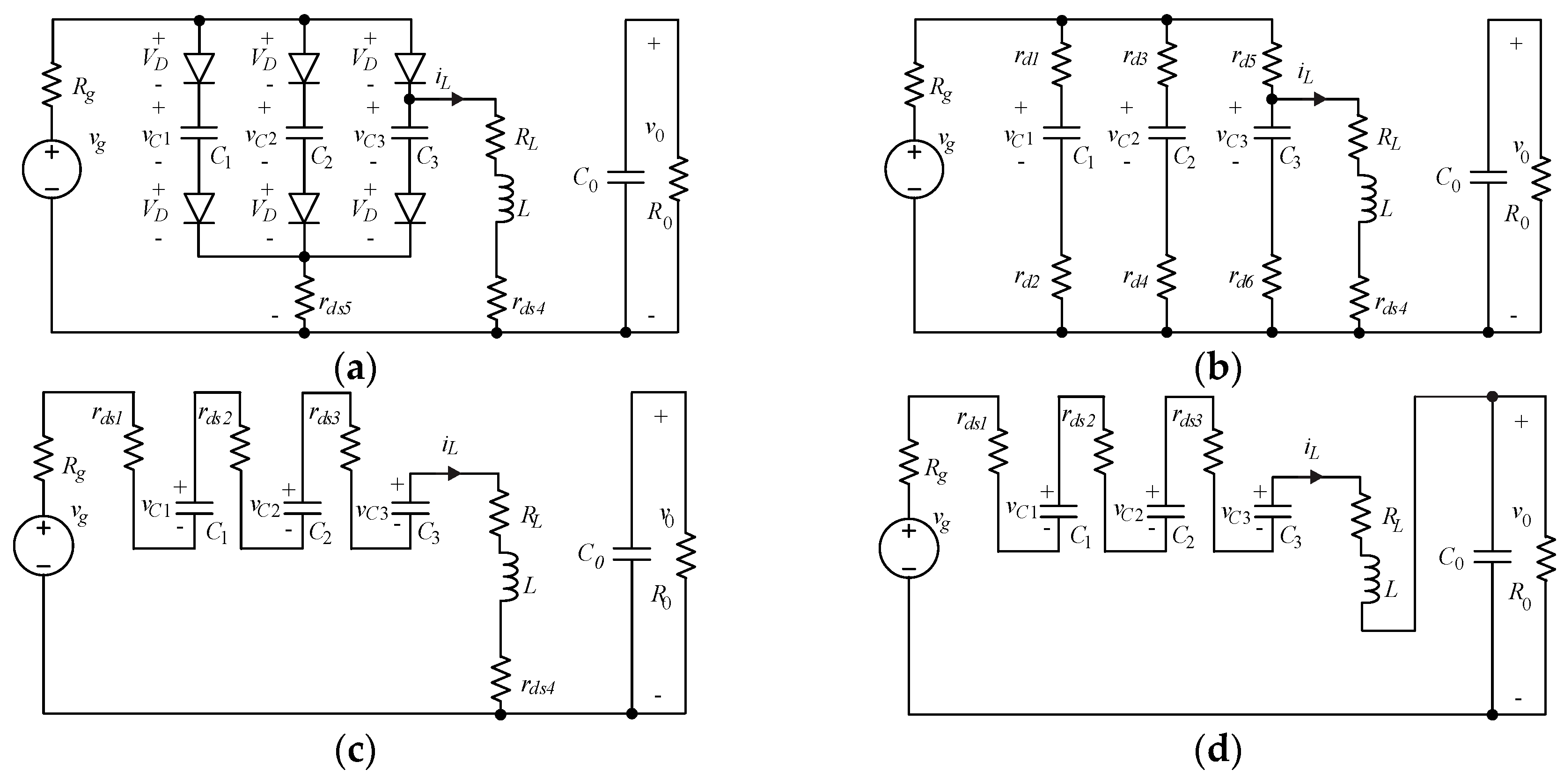
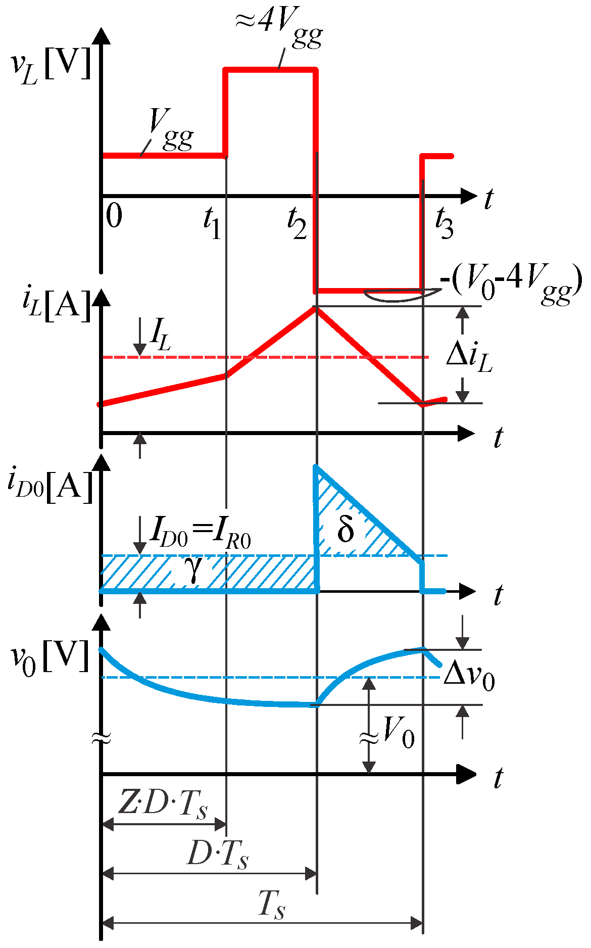
3.1. Mathematical Analysis of Diode Based SC-BC

The SC-BC [26,27] operates in three sequences, represented in the Figure 3 and Figure 4. In the first sequence, with the duration of zdTs (Figure 4a), the switches T4 and T5 are switched on and T1, T2, and T3 are switched off. The model, described by state variables vCk, iL and v0 and using an equivalent circuit, presented in Figure 3a, can be written as:
d v C k d t = 1 3 R g C k v C k 1 3 C k i L + 1 3 R g C k ( v g 2 v D ) , d i L d t = 1 L ( v C k + v D ) R L L i L , d v 0 d t = 1 R 0 C 0 v 0 .
In the second sequence, (with the duration of (1 − z)dTs, Figure 4a), T5 is switched off and transistors T1, T2, T3 and T4 are switched on. The equivalent circuit is shown in Figure 3c, and its model is represented as follows:
d v C k d t = 1 C k i L , d i L d t = 3 L v C k R g + R L L i L + 1 L v g , d v 0 d t = 1 R 0 C 0 v 0 .
In the third sequence, transistors T1, T2 and T3 (with the duration of (1 − d)Ts, Figure 4a), are switched on, and the transistors T4 and T5 are switched off, and, with the help of the equivalent circuit shown in Figure 3d, the dynamic model representing this operation mode can be written as:
d v C k d t = 1 C k i L , d i L d t = 3 L v C k R g + R L L i L 1 L v 0 + 1 L v g , d v 0 d t = 1 C 0 i L 1 R 0 C 0 v 0 .
Equation (3) describes the trajectory of state variables in time interval t ( 0 , t 1 ) , Equation (4) in interval t ( t 1 , t 2 ) and Equation (5) in interval t ( t 2 , T S ) . According the notation indicated in Figure 4, the variables z and d (duty-cycle signals) are defined as follows:
z d = { 1 , 0 t < t 1 0 , t 1 t T S and d = { 1 , 0 t < t 2 0 , t 2 t T S .
To obtain the state space average model, Equations (3)–(5) are multiplied with the duty-cycle signals’ combination zd, (1 − z)d and (1 − d), respectively. Finally, its sum represents a model of SC-BC as follows:
d v C k d t = 1 3 R g C k v C k z d 1 C k i L ( 1 2 z d 3 ) + 1 3 R g C k v g z d 2 3 R g C k v D z d , d i L d t = 1 L v C k ( 3 2 z d ) R L + R g ( 1 z d ) L i L 1 L v 0 ( 1 d ) + 1 L v g ( 1 z d ) + 1 L v D z d , d v 0 d t = 1 C 0 i L ( 1 d ) 1 R 0 C 0 v 0 .
According to the state space averaging modelling principle, the operation of the converter must be considered by introducing of small signal perturbation in the vicinity of the operating point. So, all state space variables (vCk, iL, v0), input voltage (vg) and control variables (zd, d) from Equation (7) must be described in the form of x = X + x ˜ , where X represents the average value of x, and x ˜ represents the small signal perturbation. In order to develop the model and ignoring small signal perturbations, only the average values of state space variables shall be considered, like:
V C k = 1 T S 0 T S v C k d t ; so   it   follows   v C k V C k .
Consequently, other system variables shall also be indicated only by steady state operating points, expressed by capital letters:
i L I L ;   v 0 V 0 ;   v g V g ;   v D V D ;   d D ; z d Z D .
Thus, by substituting Equations (8) and (9) into Equation (7), the large-signal non-linear dynamic model is obtained, as follows:
d V C k d t = 1 3 R g C k V C k Z D 1 C k I L ( 1 2 Z D 3 ) + 1 3 R g C k V g Z D 2 3 R g C k V D Z D , d I L d t = 1 L V C k ( 3 2 Z D ) R L + R g ( 1 Z D ) L I L 1 L V 0 ( 1 D ) + 1 L V g ( 1 Z D ) + 1 L V D Z D , d V 0 d t = 1 C 0 I L ( 1 D ) 1 R 0 C 0 V 0 .

3.2. Mathematical Analysis of MOSFET Based SC-BC

The same procedure as is described in Section 3.1 can be used to obtain the MOSFET-based SC-BC model. The diodes are replaced by MOSFETs and, in the first sequence, with the duration of zdTs (Figure 4b), the transistors T1d, T2d, T3d, T4d, T5d, and T6d, as well as switch T4 are switched on, whereas the transistors T1, T2, and T3 are switched off. Repeating the whole procedure from the previous subsection (described in Equations (3) to (10)) and replacing the model in Equation (3) of the first sequence with:
d v C k d t = 1 3 R g C k v C k 1 3 C k i L + 1 3 R g C k v g , d i L d t = 1 L v C k R L L i L , d v 0 d t = 1 R 0 C 0 v 0 ,
An average model of the MOSFET based SC-BC can be expressed by:
d V C k d t = 1 3 R g C k V C k Z D 1 C k I L ( 1 2 Z D 3 ) + 1 3 R g C k V g Z D ,
d I L d t = 1 L V C k ( 3 2 Z D ) R L + R g ( 1 Z D ) L I L 1 L V 0 ( 1 D ) + 1 L V g ( 1 Z D ) ,
d V 0 d t = 1 C 0 I L ( 1 D ) 1 R 0 C 0 V 0 .
For the MOSFET based SC-BC, a block scheme of the dynamic model is featured in Figure 5. Using Equations (12)–(14), it is possible to obtain the SC-BC gain characteristics, and also the dynamic model necessary to establish and design the control algorithms for the SC-BC inductor current IL and output voltage V0.

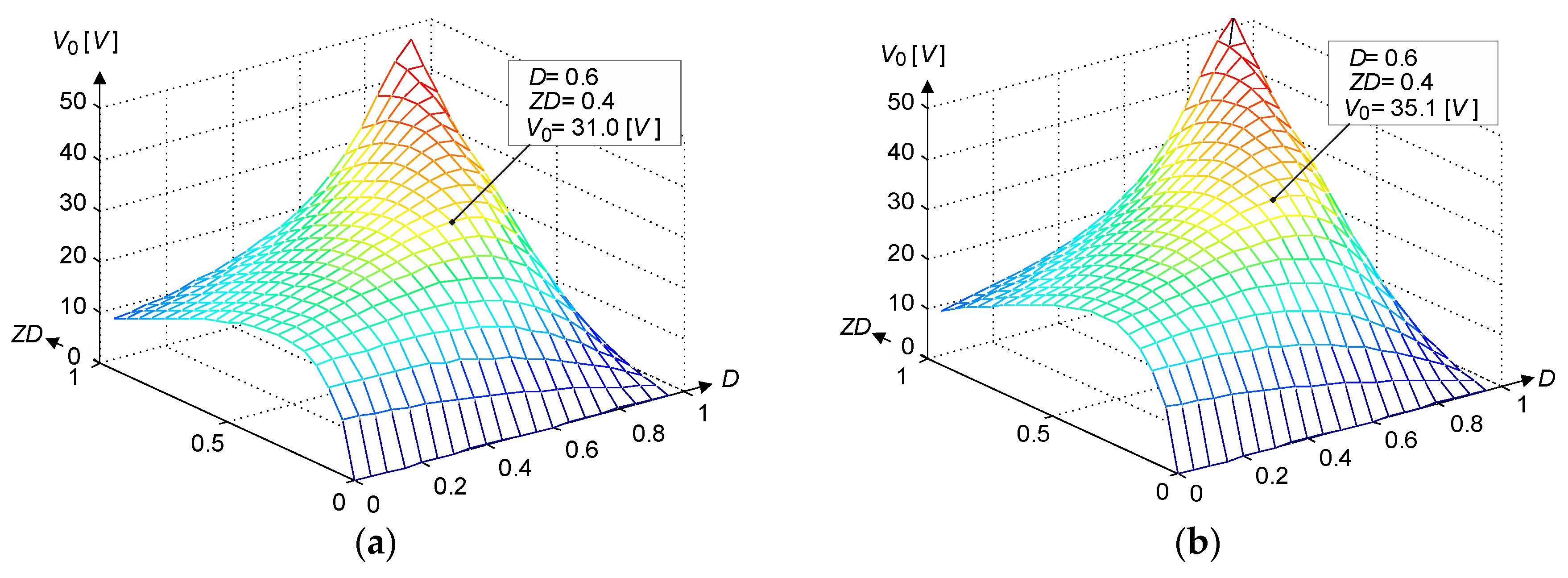
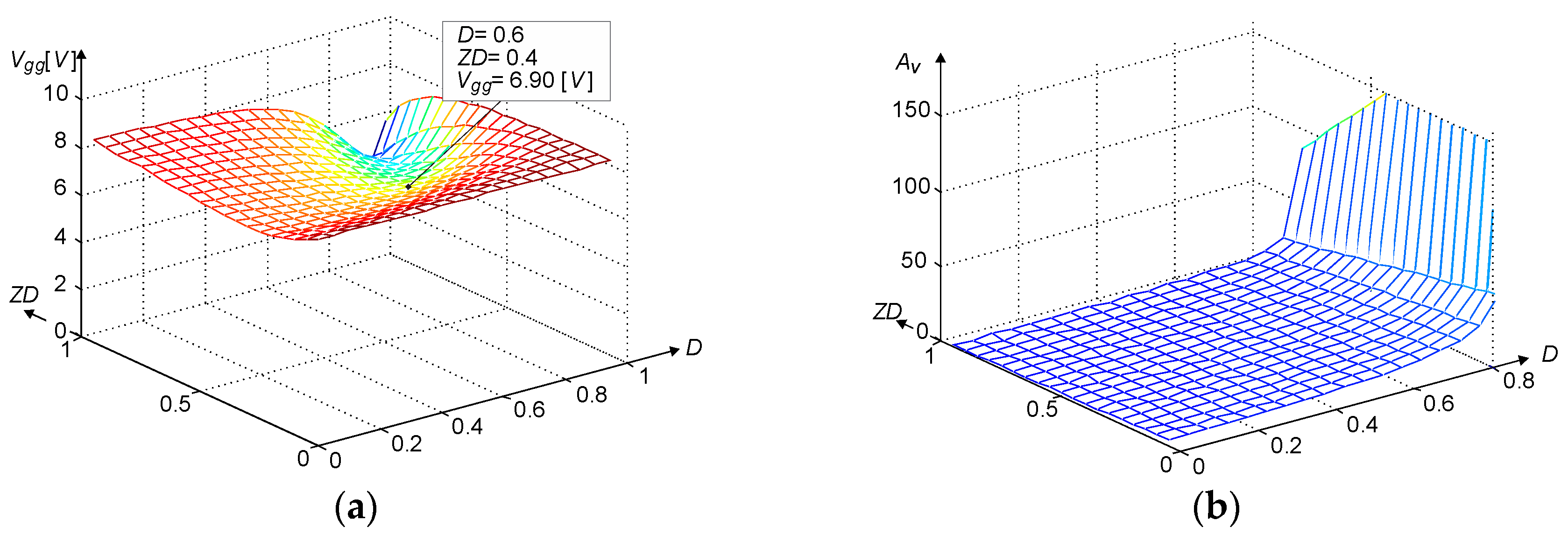
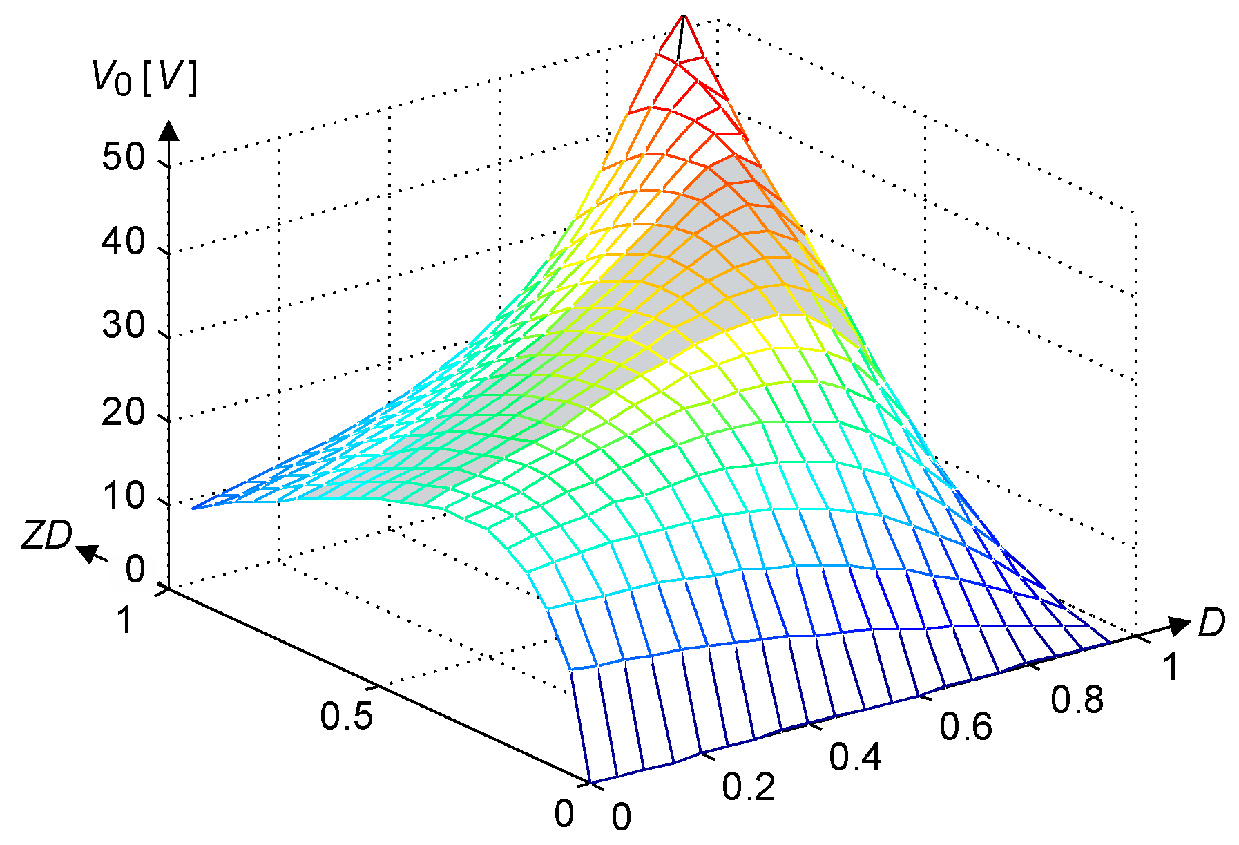
4. SC-BC Gain Characteristics

Considering Equation (10) during the steady state, all derivatives fulfil the condition:
d V C k d t = 0 ,   d I L d t = 0   and   d V 0 d t = 0 ,
The steady state value of the output voltage V0 can be evaluated for a diode based circuit from Equation (10) as is described in [26,27]:
V 0 = ( 1 D ) Z D ( 4 3 Z D ) R 0 Z D R L + ( 9 11 Z D + 3 ( Z D ) 2 ) R g + ( 1 D ) 2 Z D R 0 V g ( 1 D ) Z D ( 6 5 Z D ) R 0 Z D R L + ( 9 11 Z D + 3 ( Z D ) 2 ) R g + ( 1 D ) 2 Z D R 0 V D ,
where Vg and VD represent the average value of the open terminal TEG voltage vg and average value of the diode forward voltage vD respectively. ZD and D represent the average values of zd and d, within the interval Ts respectively, as shown in Figure 4a,b.
In the case of the MOSFET based SC-BC, the average value of the output voltage can be calculated from Equations (12)–(14) in the steady state operation (described by Equation (15)) using the same approach as presented for diode based SC-BC:
V 0 = ( 1 D ) Z D ( 4 3 Z D ) R 0 Z D R L + ( 9 11 Z D + 3 ( Z D ) 2 ) R g + ( 1 D ) 2 Z D R 0 V g .
When the result is compared to Equation (16) it can be observed that the only difference is in the absence of the second term, multiplied by the diode voltage drop VD. Based on Equations (16) and (17), the 3D-diagram is calculated and plotted by using MATLAB (v2015b, Mathworks, Natick, MA, USA). Figure 6a,b shows the calculated output voltage for diode and MOSFET based SC-BC respectively. It is evident that the MOSFET based SC-BC produces the higher output voltage, which is indicated in the chosen operational points D = 0.6 and ZD = 0.4. When observing Figure 6 and Figure 7 it shall be noted that they represent the calculated values and, in the real operation, the duty cycle D cannot be lower than ZD.
The converter static gain characteristics Av, representing the voltage gain regarding the converter input voltage, are obtained by neglecting the TEG inner resistance in Equation (17) by setting Rg 0 as follows:
A v = V 0 V g g = ( 1 D ) ( 4 3 Z D ) R 0 R L + ( 1 D ) 2 R 0 ,
where Vgg is the SC-BC input terminal voltage, and is calculated as:
V g g = V g I i n R g .
Iin is the SC-BC converter average input current. Figure 7a,b shows the changing of the input terminal voltage, which depends on all converter resistances and their operating points (Rg = 1 Ω, R0 = 70 Ω, and RL = 75 mΩ), and the SC-BC gain characteristic, respectively.
Maximal output voltage is calculated from the derivative of Equation (17), when it is rewritten to the following form:
V 0 V g = ( 1 D ) Z D ( 4 3 Z D ) R 0 Z D R L + ( 9 11 Z D + 3 ( Z D ) 2 ) R g + ( 1 D ) 2 Z D R 0 .
The value of the product ZD is considered constant, and the maximal value will be achieved for the duty cycle D, for which it is possible to claim:
( V 0 V g ) D = 0 .
The solution of this equation is:
D max = 1 Z D R 0 ( Z D R L + ( 9 11 Z D + 3 ( Z D ) 2 ) R g ) Z D R 0 ,
which is the maximal value of D. The minimal value of the duty cycle is set by the choice of ZD, because Z can not be lower than 1:
D min = Z D .
The maximal and minimal values of the available output voltage V0 can, thus, be calculated if Dmax and Dmin are introduced into the Equation (20)). These values have to be applied as the dynamic limits (dependent on the chosen ZD) of the control algorithm output in order to ensure the stability of operation.

5. Choice of SC-BC Passive Elements

The main passive elements, as are inductor L, capacitors C0 and Ck, in the SC-BC need to be chosen based on the requirements set to the SC-BC circuit. Figure 8 shows ideal waveforms of the necessary inductor current iL and output voltage v0, together with the inductor voltage vL and the current iD0 passing the diode D0.
The procedure for the choice of inductor and output capacitor is based on the approach described in [30], utilising the inductor current and output voltage ripple. When steady state of the SC-BC operation is achieved, the inductor current ripple can be evaluated by observing the inductor current curve in time interval t ( t 2 , t 3 ) , as indicated in Figure 8:
i L ( t ) = i L ( t 2 ) V 0 4 V g g L ( t t 2 ) .
Regarding the current waveform, it can be noted that i L ( t 2 ) = I L , m a x and i L ( t 3 ) = I L , m i n , therefore the current ripple is defined as:
Δ i L = I L , min I L , max = V 0 4 V g g L ( t 3 t 2 ) Δ i L = V 0 4 V g g L ( 1 D ) T s ,
where the time interval is calculated as t 3 t 2 = ( 1 D ) T s . By dividing both sides of Equation (25) by IL, it can be rewritten as:
Δ i L I L = V 0 4 V g g L I L ( 1 D ) T s ,
Using the power balance (the input of BC stage of SC-BC is ideally equal to the output of SC-BC), the following is obtained:
V g g * I L = V 0 I 0 , I 0 = V 0 R 0 I L = V 0 2 R 0 V g g * ,
where V g g * is the input of the boost stage of SC-BC, which, under the assumption that V g g V C k , can be rewritten in the following form:
V g g * = V g g Z D + ( V g g + 3 V C k ) ( 1 Z D ) ( 4 3 Z D ) V g g .
Equation (28) is introduced to Equation (27):
I L = V 0 2 R 0 ( 4 3 Z D ) V g g ,
and Equation (26) is rewritten as:
Δ i L I L = V 0 4 V g g L V 0 2 ( 1 D ) ( 4 3 Z D ) V g g R 0 T s ,
from which the following inequity can be derived:
L ( V 0 4 V g g ) ( 1 D ) ( 4 3 Z D ) V g g R 0 T s   Δ i L I L V 0 2 .
According to the inductor current ripple (40%), choice of operation point and uncertainty of the parameters: V 0 = 32   V , V g g ( 6 V , 8.6 V ) , R 0 ( 55 Ω , 100 Ω ) , Z = 0.6, D = 0.6 and Ts = 10 μs (switching frequency is fs = 100 kHz), the following inequity is used to choose the inductance:
L 272 μ H .
For further consideration the value L = 330 μH was chosen.
As also follows from [30], the capacitance C0 value can be chosen using the voltage waveforms featured in Figure 8 by blue colour. The area described by γ represents the charge Δq, which discharges the capacitor C0 from v 0 ( 0 ) = v 0 , m a x to v 0 ( t 1 ) = v 0 , m i n . During this time, the capacitor C0 is discharged with the current IR0. The voltage ripple can be calculated as follows:
Δ v 0 = V 0 , m a x V 0 , m i n = Δ q C 0 = I R 0 D T s C 0 = V 0 R 0 C 0 D T s ,
which can be rewritten to represent the output voltage ripple:
Δ v 0 = V 0 R 0 C 0 D T s Δ v 0 V 0 = D T s R 0 C 0 .
After rearrangement of Equation (33) the inequality for the choice of capacitor can be presented:
C 0 D T s R 0 ( Δ v 0 V 0 ) .
Using the obtained inequality in Equation (34) the capacitance was evaluated to be (for Δ v 0 = 2 % ):
C 0 22 μ F .
For further analyses the C0 = 40 μF was chosen.
The energy approach was used for the calculation of Ck. The main idea of this approach is that the inductor receives from the SC capacitors the difference in energy required for its charging.
W L = W C k 3 C k V C k 2 2 = L ( I L , m a x 2 I L , m i n 2 ) 2 .
Taking into account the assumption that V g g V C k , the following equation is derived:
3 C k V g g 2 = L ( I L , m a x 2 I L , m i n 2 ) ,
which can be rewritten as:
3 C k V g g 2 = L ( I L , m a x + I L , m i n ) ( I L , m a x I L , m i n ) ,
where the sum of maximal and minimal inductor current values is represented with the average inductor current value, and the difference of these two values represents the inductor current ripple:
I L = 1 2 ( I L , m a x + I L , m i n ) , Δ i L = I L , m a x I L , m i n .
Equation (37) can now be represented as:
3 C k V g g 2 = 2 L I L Δ i L
and the capacitance Ck can be chosen on the basis of the following inequity:
C k = 2 L I L Δ i L 3 V g g 2 .
The capacitance Ck was, thus, evaluated to be:
C k 19 μ F .
For further analyses the value Ck = 20 μF was chosen.

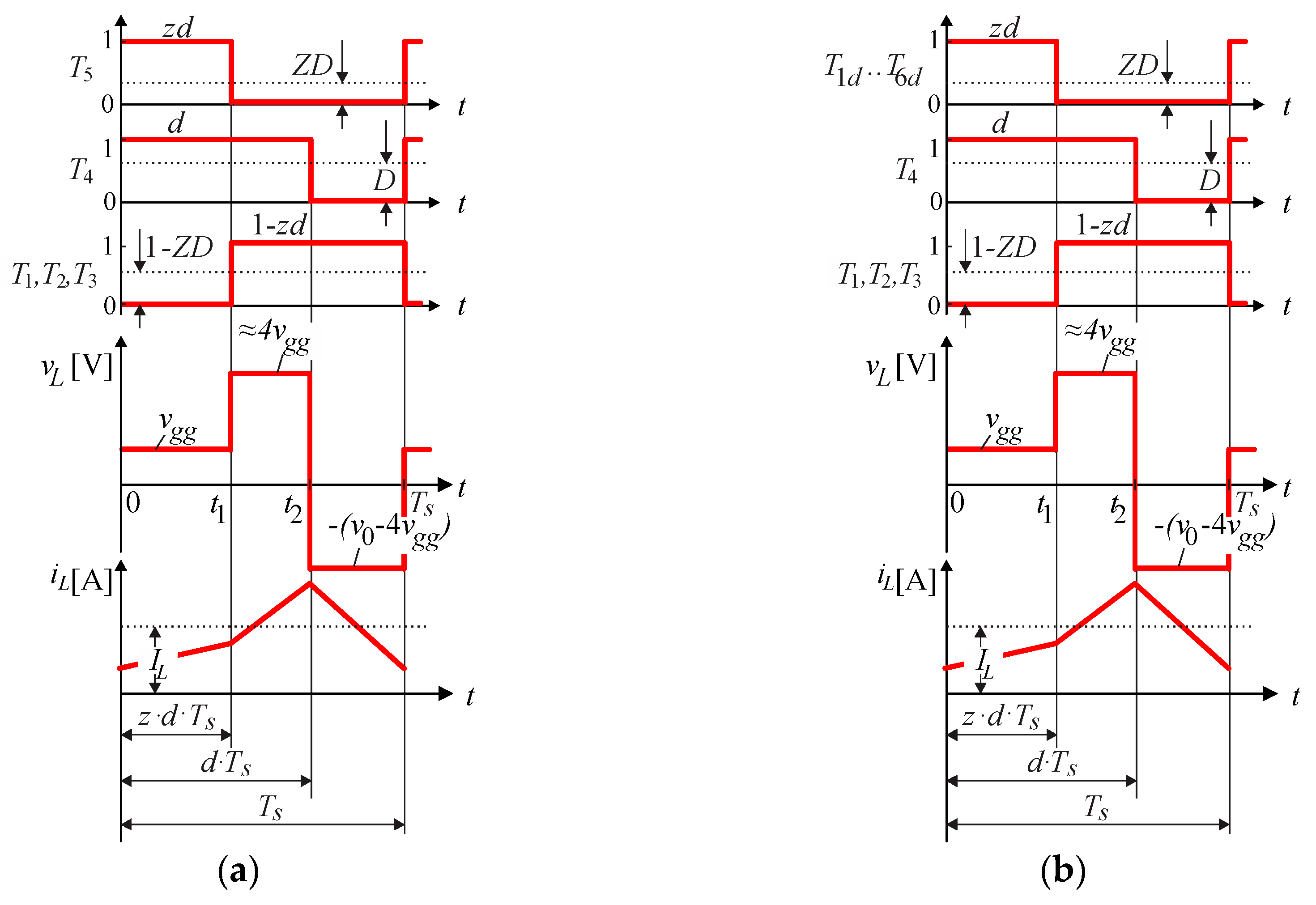
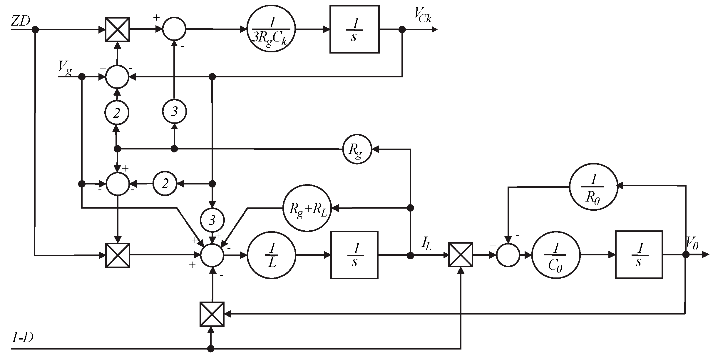
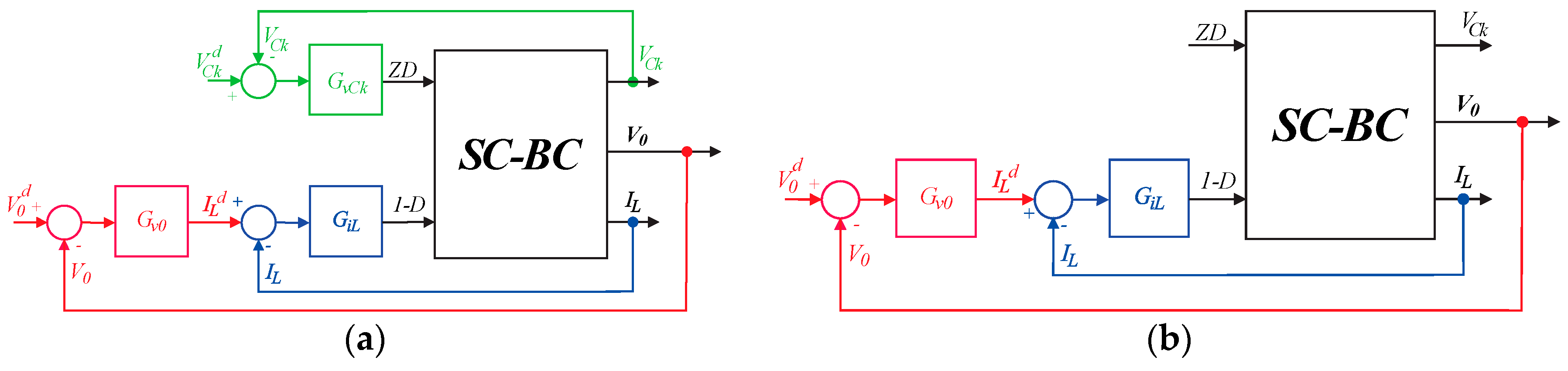
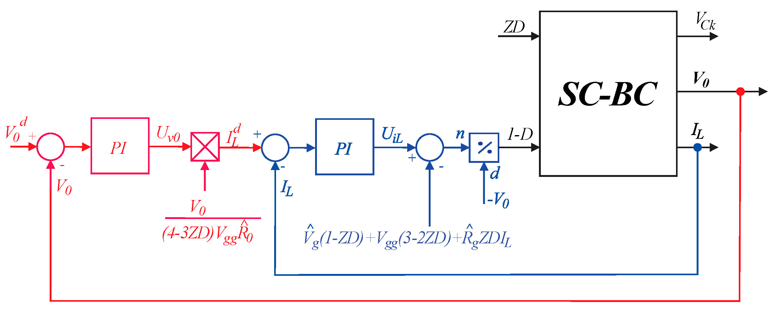
6. Control Algorithm

The control algorithm was developed for the MOSFET-based converter. A cascade control structure can be used for the control of the SC-BC, as presented in Figure 9a. The inductor current IL is controlled in the inner loop, and the output voltage V0 is controlled in the outer loop. The desired output voltage V 0 d is set by the user or the supervising system, whereas the desired value of the inductor current I L d is provided as an output of the voltage controller Gv0. The output of the inductor current controller GiL is the duty cycle D. In some cases, when only the current control is required, as is the case when the TEG-powered power harvesting system is connected in parallel to another power source (for example a PV source), the inductor current control can be sufficient. Switched capacitor circuit voltages VCk can be controlled separately, almost independently from the aforementioned control; the output of the control is ZD, the switched capacitor charging duty cycle Z, multiplied by the duty cycle D, but the product can be applied as a separate variable, and it is only important to assure that the duty cycle D is not too small, i.e., lower than ZD, which can be achieved by setting of the controller limits (described in Equations (22) and (23)).
It would only be required to measure one of the switched capacitors circuit voltages, because the symmetry of the legs is provided by the adequate design. However, the measurement can be a cost issue and not practical (based on findings in [26] control of vCk could even result in reduced efficiency), so the value of ZD can be set as a constant, as is the case for further simulation and experimental verification of the algorithms. In this case, the control scheme is featured in Figure 9b. The control algorithm of the SC-BC was developed using the linearization method as presented in [28,29]. It was developed on the base of the derived system model in Equations (12)–(14).

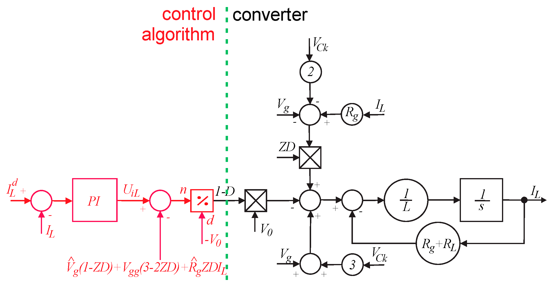
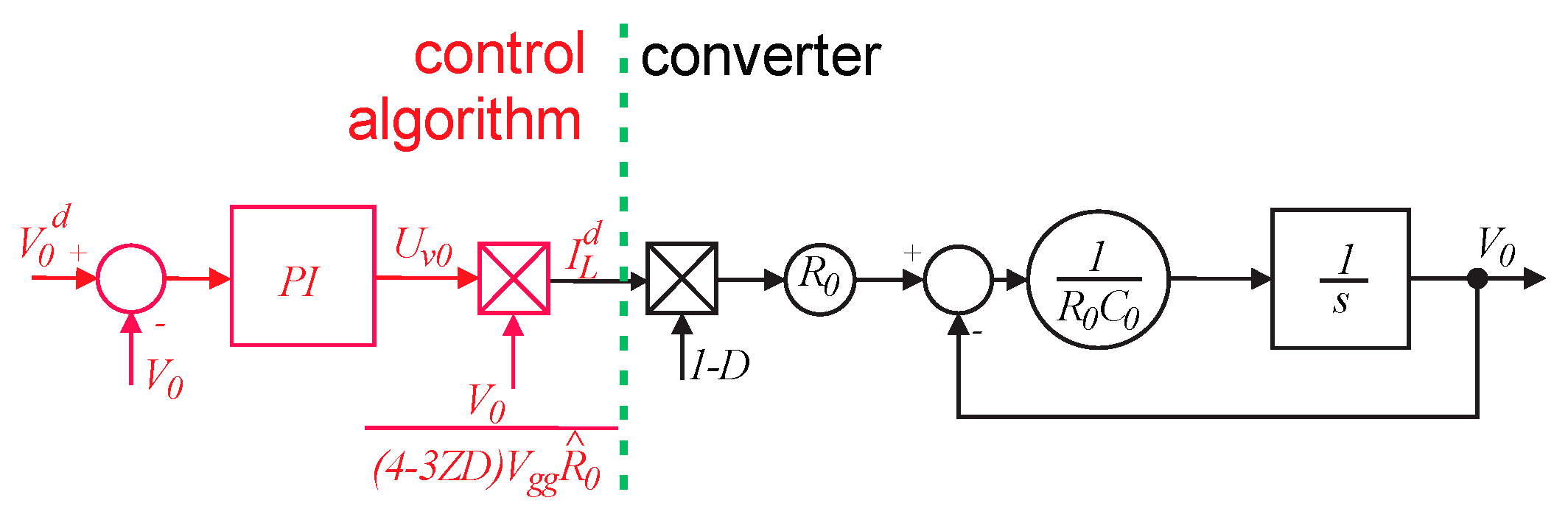
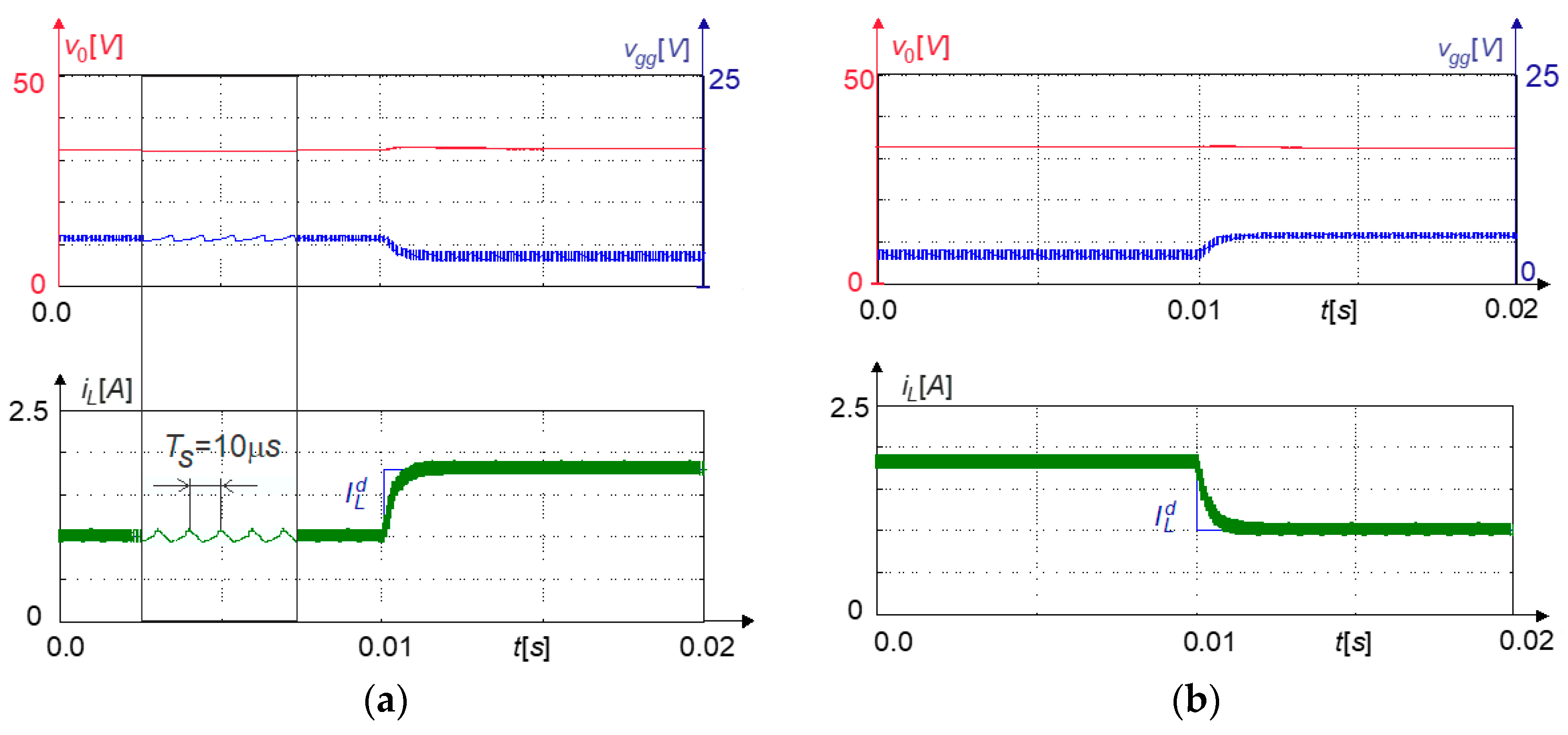
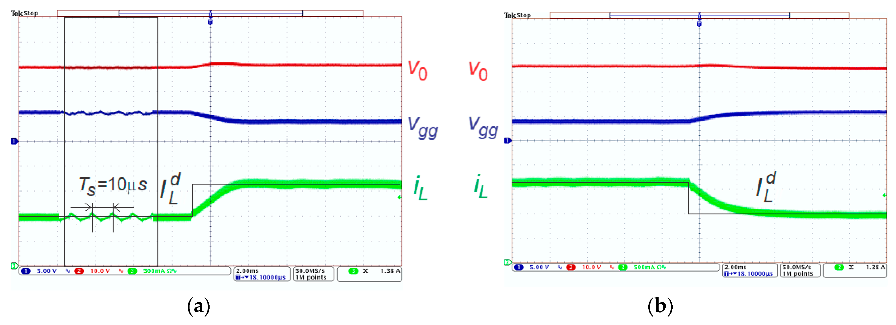
6.1. Control of Inductor Current IL

The model of the inductor current in Equation (13) can be rewritten as:
L d I L d t + ( R L + R g ) I L = V g ( 1 Z D ) + V C k ( 3 2 Z D ) + R g Z D I L V 0 ( 1 D ) .
The dynamic behaviour of the inductor current is highly nonlinear, and the use of a simple linear controller (for example a PI controller) would not be sufficient to assure a sufficiently precise and robust control. The solution of this problem is to linearise the nonlinear model in Equation (41) and apply the linear controller to the linearised model. In the first step it can be assumed that voltages on the capacitors Ck do not differ much from the converter input voltage V g g   · ( V C k V g g ) , thus Equation (41) can be rewritten as:
L d I L d t + ( R L + R g ) I L = V g ( 1 Z D ) + V g g ( 3 2 Z D ) + R g Z D I L V 0 ( 1 D ) .
The value of the duty cycle can now be calculated from:
1 D = 1 V 0 ( U i L ( V ^ g ( 1 Z D ) + V g g ( 3 2 Z D ) + R ^ g Z D I L ) ) ,
where ^ represents the estimated values, V ^ g is the estimated value of the open terminal TEG voltage, and R ^ g the estimated value of the inner TEG resistance. UiL represents the control variable, and is defined as an output of the PI controller, which will be used as the abovementioned linear controller. If it is assumed that TEG parameters are well known ( V ^ g = V g and R ^ g = R g ) and the SC capacitor voltage equals the TEG terminal voltage ( V C k = V g g ), the model in Equation (41) can be represented as a linear system:
L d I L d t + ( R L + R g ) I L = U i L ,
which, as a result, gives the following transfer function to be controlled by the linear PI controller:
I L ( s ) U i L ( s ) = 1 s L + ( R L + R g ) ,
where UiL(s) and IL(s) are Laplace transforms of the UiL and IL, respectively.
A block scheme is featured in Figure 10, where the controlled system is depicted in black, and the control algorithm in red colour. In order to perform the control algorithm, it is necessary to measure converter input and output voltage Vgg and V0, respectively, and inductor current IL.
The PI controller for the inductor current control is represented with the following transfer function:
U i L ( s ) I L d ( s ) I L ( s ) = K p i L 1 + s T i i L s T i i L ,
where KpiL is the controller gain, and TiiL the controller time constant. I L d ( s ) is the Laplace transform of I L d . The design of the controller, i.e., calculation of the parameters (the chosen values were KpiL = 0.5 and TiiL = 55 μs), is straightforward, and will not be described here. It is performed based on the assumption that the control plant is represented by Equation (44), and is thus represented by the transfer function in Equation (45).
The variation of TEG parameters, open terminal voltage Vg and internal resistance Rg can be described as additive disturbance δiL in the control loop. If taken into consideration, Equation (44) has the following form:
L d I L d t + ( R L + R g ) I L = U i L + δ i L ,
where the disturbance can be represented using Equations (41) and (42):
δ i L = ( V g V ^ g ) ( 1 Z D ) + ( V C k V g g ) ( 3 2 Z D ) + ( R g R ^ g ) Z D I L .
It is assumed that the TEG terminal voltage and SC capacitor voltage have almost the same value and the value of duty cycle ZD is known. TEG terminal voltage and inductor current are measured with sufficient precision. Thus, it can be observed that the value of disturbance is small, and, therefore, it should not present a problem. The behaviour of the control algorithm in the case of its presence can be described with the transfer function showing the disturbance rejection performed by the PI controller:
U i L ( s ) δ i L ( s ) = s T i i L s 2 L + s ( R g + R L + K p i L T i i L ) + K p i L ,
from which it is obvious that the disturbance due to the TEG parameter variations will be completely rejected in a finite time.

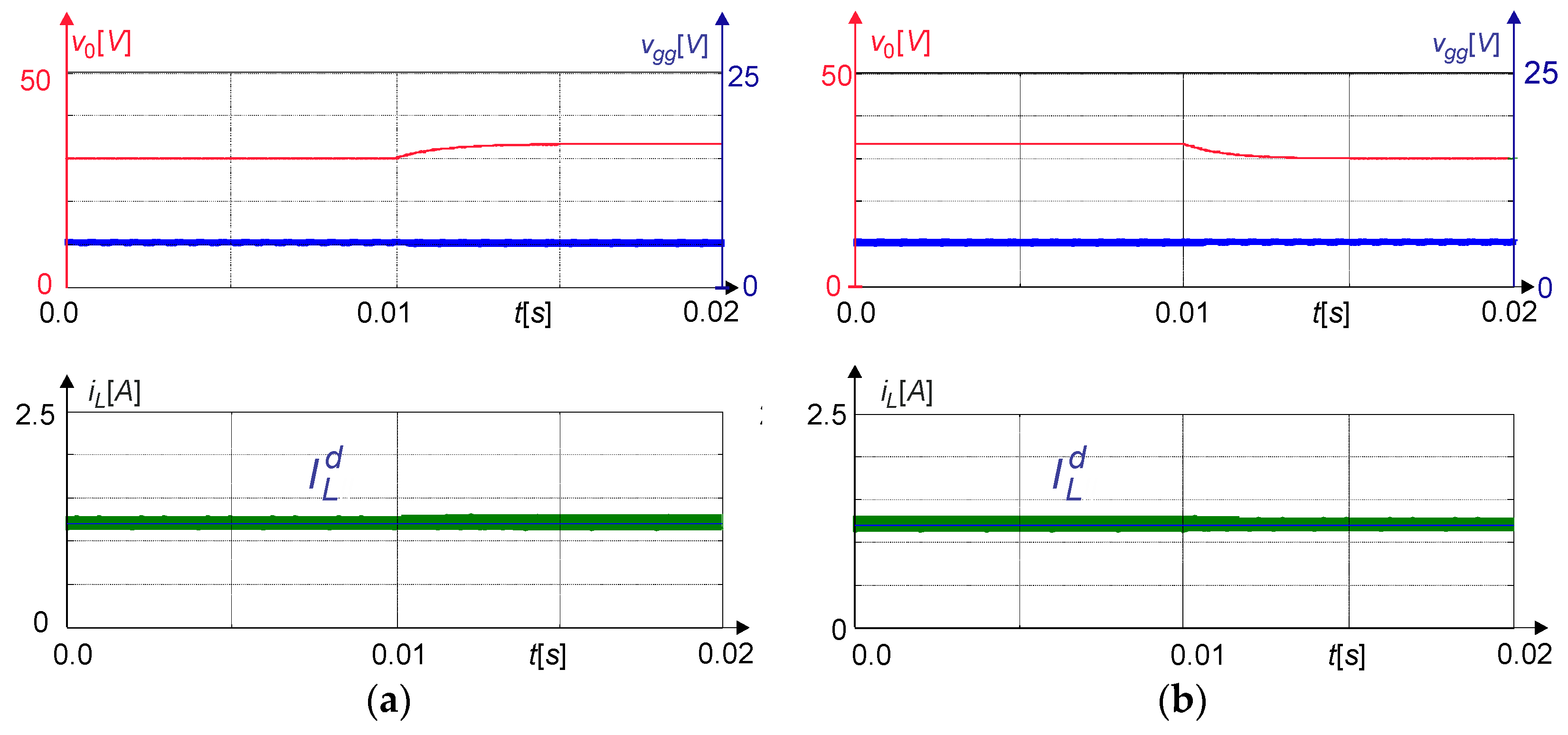
6.2. Control of Output Voltage V0

The control scheme for the output voltage is derived using the same methodology as the one for the inductor current control. The nonlinear model represented by Equation (14) is first linearised, and, in the second step, the linear controller is applied as a feedback controller of the linearised model.
The model of the output voltage in Equation (14) can be rewritten as:
R 0 C 0 d V 0 d t + V 0 = R 0 I L ( 1 D ) .
Based on the ideal voltage gain value represented in Equation (18), where RL is neglected, the value of the duty cycle ( 1 D ) can be substituted as follows:
( 1 D ) = ( 4 3 Z D ) V g g V 0
and Equation (50) can be rewritten as:
R 0 C 0 d V 0 d t + V 0 = ( 4 3 Z D ) V g g V 0 R 0 I L d .
The model in Equation (52) remains nonlinear, and linearization is performed by applying the inverse function of idealised voltage gain (Equation (51)) to its input, deriving the desired value of inductor current using the following formula:
I L d = V 0 ( 4 3 Z D ) V g g R ^ 0 U v 0 ,
where R ^ 0 represents the estimated value of the load resistance, and Uv0 is the control variable representing the output of the linear controller to be used as a feedback controller. The model presented in Equation (50) can now be rewritten as:
R 0 C 0 d V 0 d t + V 0 = U v 0 ,
The transfer function of the linearised system can now be represented as:
V 0 U v 0 = 1 s R 0 C 0 + 1 ,
where Uv0(s) and V0(s) are Laplace transforms of the Uv0 and V0, respectively. Graphical representation is featured in Figure 11, where the control algorithm is depicted in red and the controlled system in black.
The PI controller is represented with the following transfer function:
U v 0 ( s ) V 0 d ( s ) V 0 ( s ) = K p v 0 1 + s T i v 0 s T i v 0 ,
where Kpv0 is the controller gain and Tiv0 the controller time constant. V 0 d is the Laplace transform of the V 0 d . The design of the controller, i.e., calculation of the parameters (in the presented case the values Kpv0 = 3.2, Tiv0 = 4.8 ms were chosen), is again straightforward, and will not be described here. It was performed based on the assumption that the control plant is represented by Equation (54) and its transfer function is represented by Equation (55). A detailed block scheme of the complete control is given in Figure 12.
The variation of TEG parameters, open terminal voltage Vg and internal resistance Rg in this case have no obvious impact on the control behaviour. Taking into account Equations (18) and (53), and neglecting the internal resistance of the inductor, Equation (52) can be rewritten as:
R 0 C 0 d V 0 d t + V 0 = R 0 R ^ 0 U v 0 .
It can be observed that the load resistance R0 is the main parameter with an impact on the precision. The input-output behaviour of the output voltage control loop can be represented by the following transfer function:
V 0 ( s ) V 0 d ( s ) = s T i v 0 + 1 s 2 T i v 0 R 0 C 0 R ^ 0 R 0 K p v 0 + s ( T i v 0 + T i v 0 R ^ 0 R 0 K p v 0 ) + 1 .
Based on the transfer Equation (58) it can be assumed that the control behaviour should remain stable, even in the case of a significant variation of load resistance, if the PI controller gain Kpv0 is chosen to perform a slightly more conservative control, i.e., its value is not set to the upper available limit. The precision of the control is achieved, because no static error will occur.

7. Results

A 30 W experimental prototype of the proposed MOSFET-based SC-BC was built, and the experimental results were carried out to prove the performed analysis of the static and dynamic behaviour of the converter. The experimental setup of the SC-BC is shown in Figure 13 with N-type MOSFETs (FDS5672) and appropriate passive components. In the experimental system the following values were chosen for the SC-BC parameters: L = 330 µH, RL= 75 mΩ, Ck = 20 µF and C0 = 40 µF. The basic value of load was set to R0 = 60–100 Ω. The TEG parameters were Vg = 8.6 V, Rg = 1 Ω. Based on the state space averaging method, the converter gain characteristics were investigated, and, using the same approach, also the control algorithm, based on the non-linear compensation, was investigated. The results presented in this paper focus only on the SC-BC; the behaviour of the TEG is not evaluated. The TEG parameters are considered in the control design and in the evaluation of the parameter variation related disturbance rejection.

7.1. Verification of Gain Characteristics

The SC-BC gain characteristics (output voltage as a function of duty cycles ZD and D) is represented in Figure 14. In order to verify it, a specific area in the calculated gain characteristics was chosen (Figure 14, grey shadowed), and the calculated results were compared to the measured ones. Measured results are presented in Table 1, whereas comparison of measured and calculated values is shown in Figure 15a,b. When observing Figure 14 it shall be noted that it represents the calculated values, and, in the real operation the duty cycle D cannot be lower than ZD.
For measurement verification the control variable ZD was chosen as ZD = 0.4, and ZD = 0.5, respectively, and for every chosen ZD, the control variable D was changed within the area D ( 0.4 , 0.9 ) . It is important to note that in the real operation the value of duty cycle D can only be higher than ZD, because Z can only be lower than or equal to 1. Duty cycle D is also limited to the maximal value, as was determined in Equation (22), and is approximately at D = 0.7. In the simulations and experimentation, from which the results in the following text were obtained, Equation (22) was used for the on-line calculation of the D upper limit. As a result of this limitation the available range of output voltage is also limited. Based on the measurement results collected in Table 1, the maximal distance between measurement points and theoretical calculated curve (represented as performance index ε ), was evaluated as ε = ± 2.5 % . The measurement points are indicated by green dots, and theoretical calculated curves are drawn in blue, and are shown in Figure 15a,b. According to the thermal properties of inner and output resistance (Rg and R0), the gain analysis performed in Section 4 is sufficiently precise for further study, for example, for study and introduction of the Maximum Power Point Tracking (MPPT) algorithms. According to the theoretical calculation and measurement, it can be concluded that the developed gain model gives representative results.

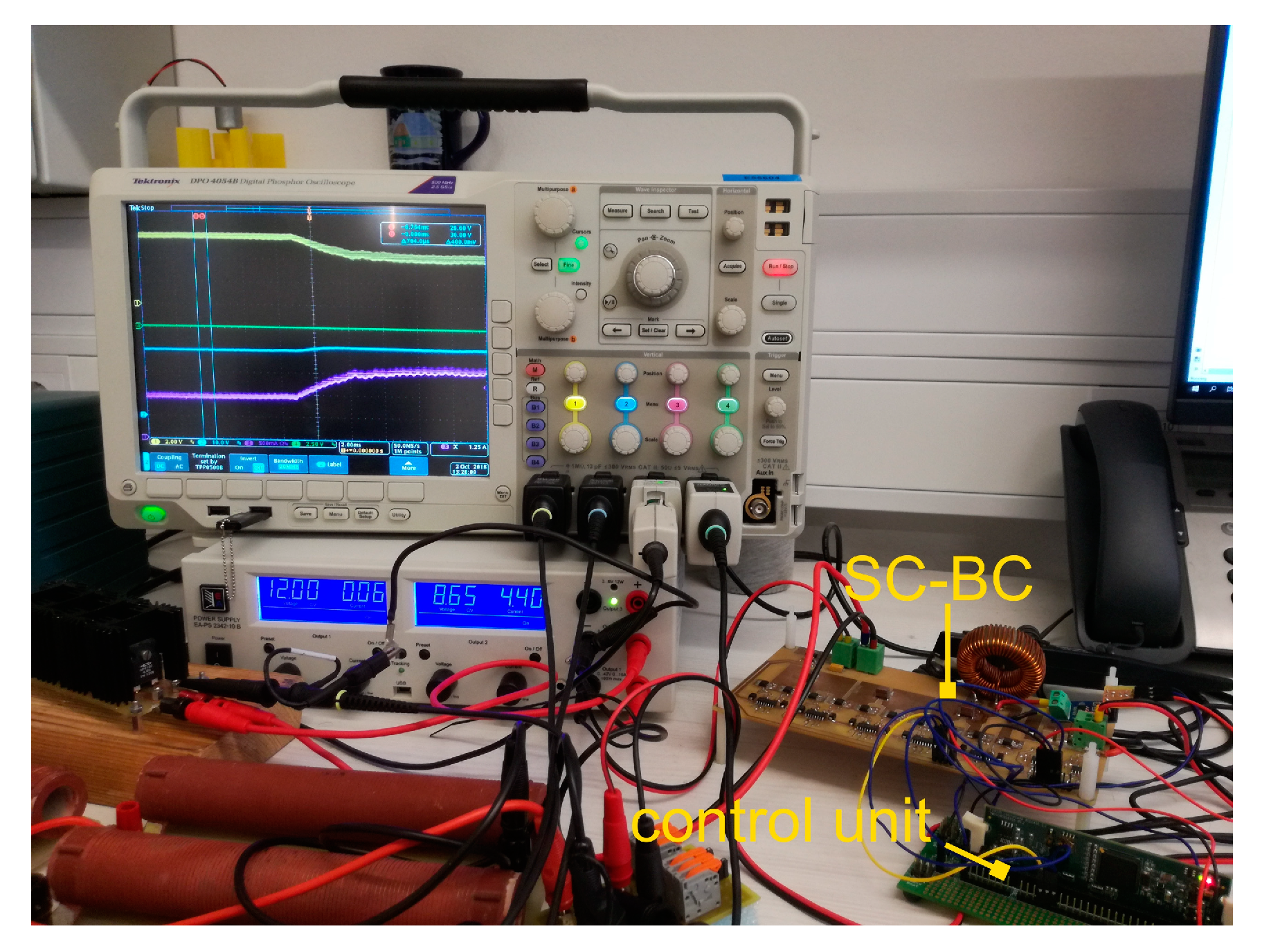
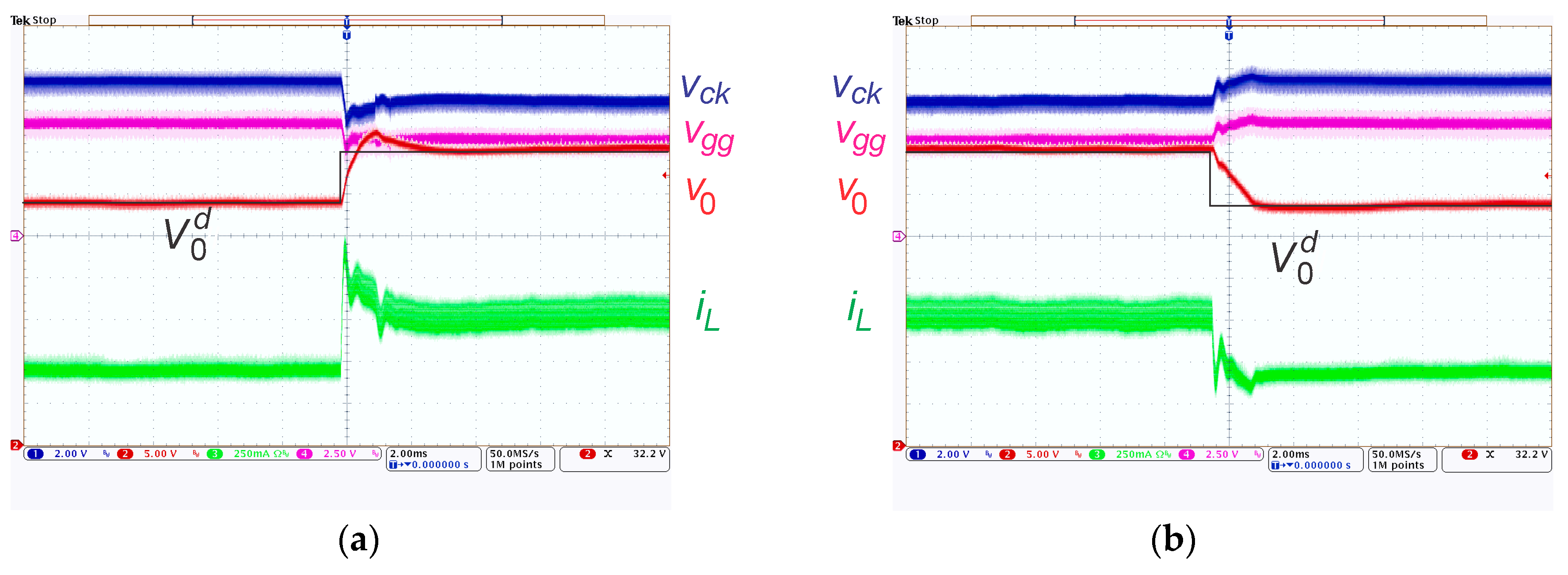
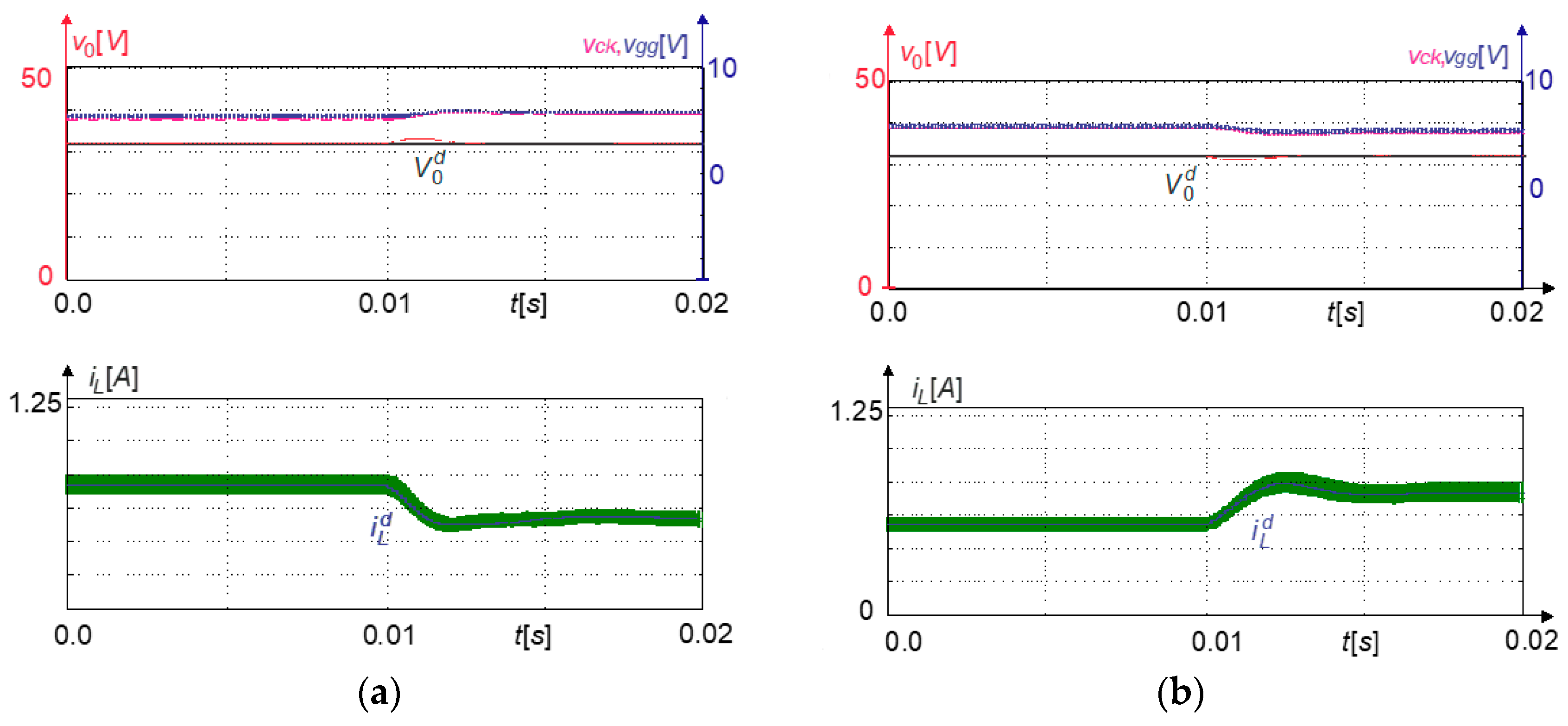
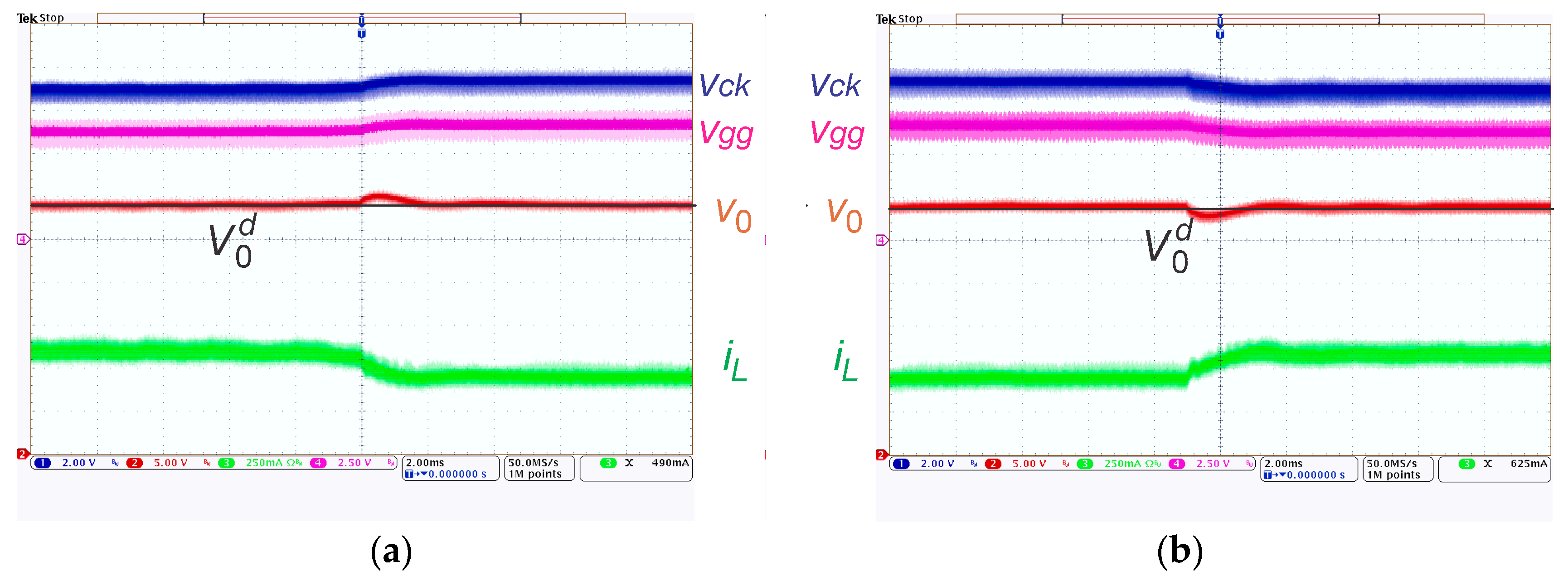
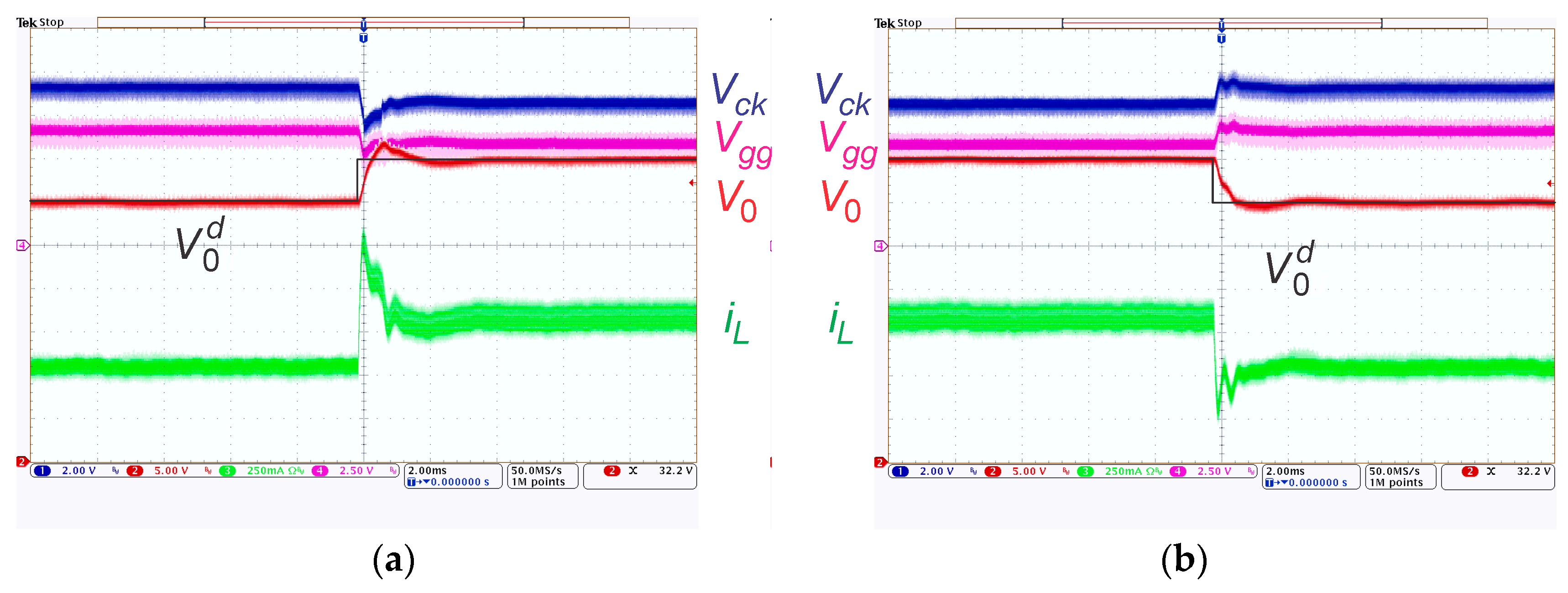
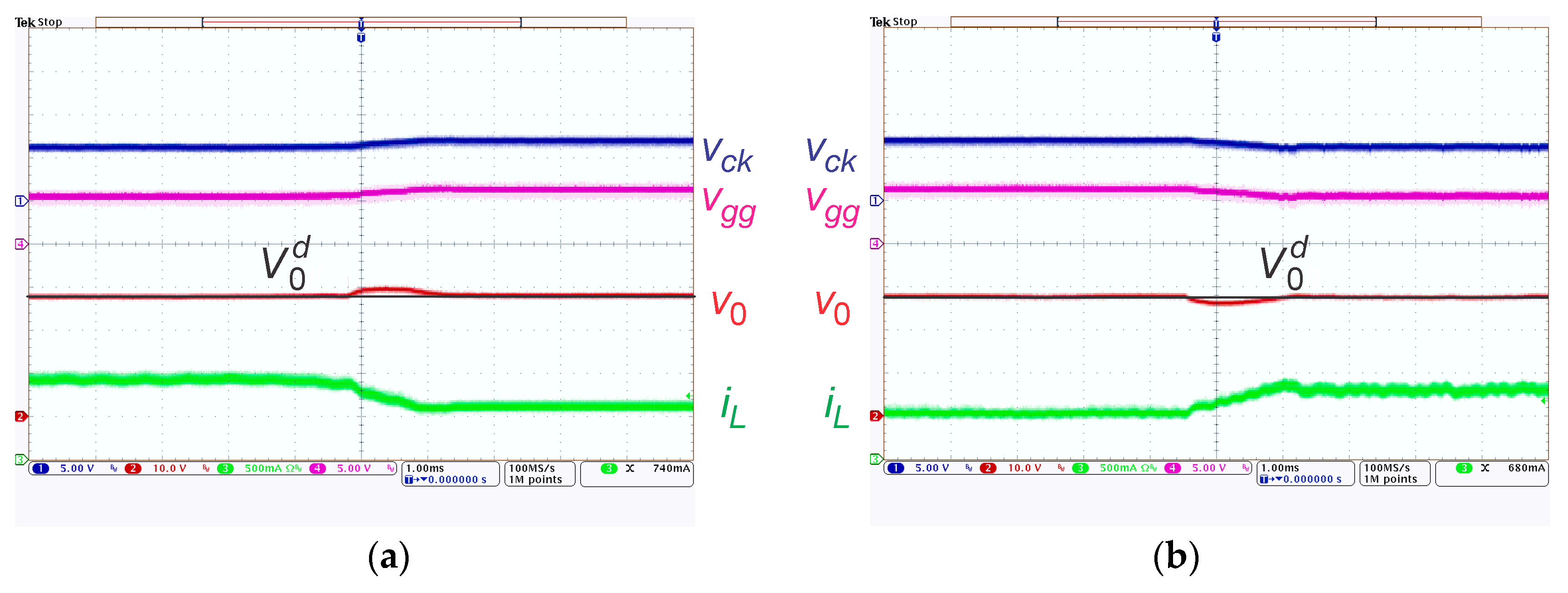
7.2. Control Algorithm Verification, Simulation and Experimentation

In order to evaluate the behaviour of the control algorithm, simulations and experiments were performed for the inductor current and output voltage control. MATLAB/Simulink was used for the simulations, specifically the SimPowerSystems Toolbox. The discrete time control was applied to emulate the behaviour in the case of the experiments. The system model used in simulations applied the realistic parameters of the converter. As was proven by results in the following text, the simulation model resembles the operation of the real SC-BC DC-DC converter adequately. In experimentation, the control algorithm was implemented using a digital signal controller, TMS320F28335 by Texas Instruments (Dallas, TX, USA), programmed using the MATLAB/Simulink Embedded Coder (for Texas Instruments C2000 microcontrollers). Both simulations and experimentation were first performed for the control of inductor current iL, and then for the output voltage v0. In the case of output voltage control, the inductor current control was used as the inner control loop, as represented in Figure 11.
It is important to note that the operation of the SC-BC is limited regarding the range of both inductor current and output voltage. The limitations are due to the boost converter operation, where the output voltage value cannot be below the input voltage value, whereas the static characteristics (Figure 15) limit the maximal value of the output voltage. This behaviour is also reflected in the available range of inductor current, where the minimal and maximal values also limit the operation. The converter is strictly unidirectional. The behaviour regarding the limits is dependent on the set value of the ZD.

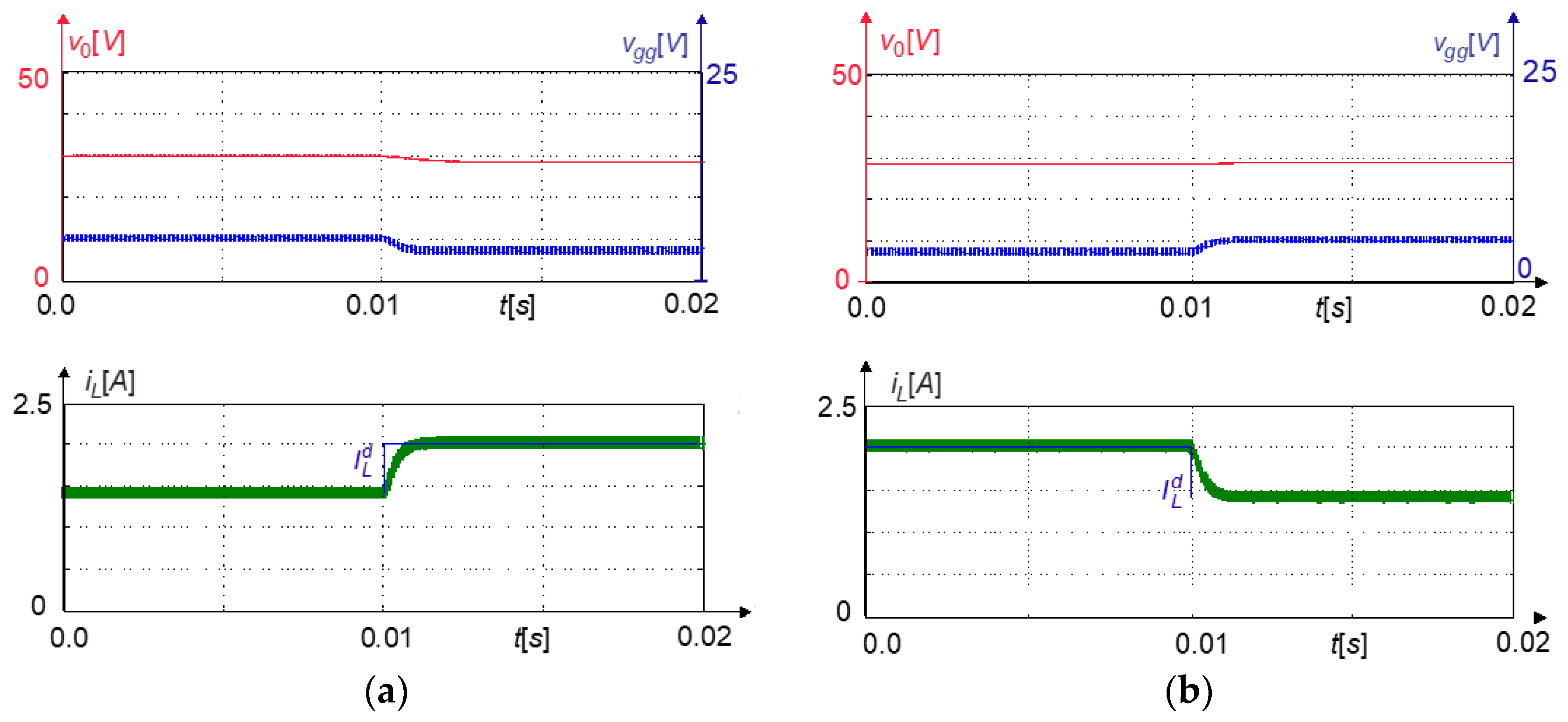
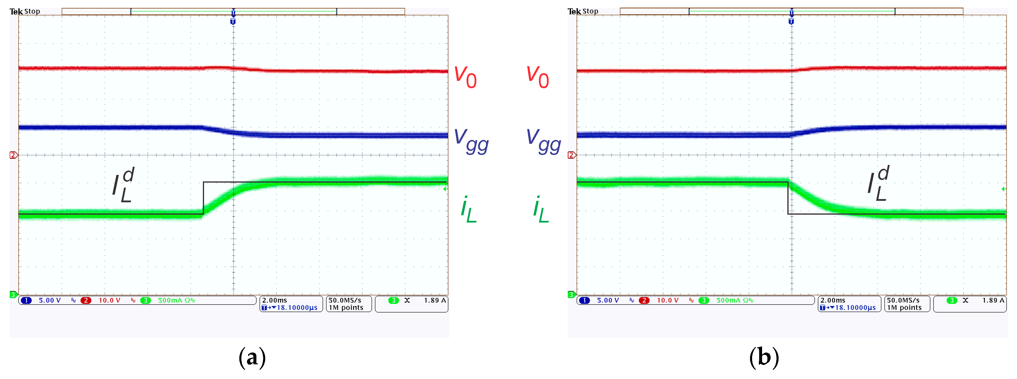
7.2.1. Inductor Current Control

The current control was first investigated with the simulations and, later, with the experimentation. During the current control, the whole system was organised as a current source to support the PV DC voltage. The output current IR0 (current through the load R0) was controlled implicitly by controlling the inductor current, so the full attention was concentrated to the inductor current control. Figure 16 shows the simulation results, and Figure 17 the experimental results when ZD = 40%, output resistance was R0 = 70 Ω, and TEG open terminal voltage was Vg = 8.65 V. For the simulation results in Figure 16, the top graph shows the output voltage v0 and converter input voltage (TEG output voltage) vgg. The output voltage v0 is represented in red, and the converter input voltage vgg in blue. On the bottom graph, the inductor current is represented, the reference value I L d in blue and the actual value iL in green. The same presentation (top and bottom graphs) and colour scheme are used for the representation of the same values in the case of the experimental results shown in Figure 17, with the exception of I L d , which is represented in black.
A precise tracking of the inductor current is presented in both cases, in simulations and experiments. In the case of the increased reference value of the inductor current iL, the input current demand was also increased, thereby reducing the value of the converter input voltage vgg, due to the voltage drop on the TEG inner resistance Rg. To represent the behaviour of the converter better, the cut-out of the voltages and currents is represented, showing the behaviour of the variables in the smaller time measure. The behaviour as represented in Figure 4b can be observed for the inductor current in the cut-out for both simulations and experimental results. The input voltage of SC-BC was proven to exhibit only a moderate ripple. At this point, it is important to note that the resistances of capacitors and MOSFETs were not considered in the control design process, and the TEG internal resistance was not known with a very high precision. Thus, the stable operation in the case of experimental results also proves the robustness of the control to the variations of Rg.
The operation under the changing load condition is represented in Figure 18 and Figure 19, when ZD = 40% and current reference was set to I L d = 1.2 A. TEG open terminal voltage was again Vg = 8.65 V. Figure 18 features the simulation results, and the experimental results are presented in Figure 19. Transients in the case of output resistance R0 changing from 60 Ω to 80 Ω are represented in Figure 18a and Figure 19a, whereas Figure 18b and Figure 19b represent the behaviour in the case when the output resistance R0 changed from 80 Ω to 60 Ω. Again, for both simulation and experimental results, the top graph shows the output voltage v0 and converter input voltage (TEG output voltage) vgg, where the output voltage is represented in red and the converter input voltage in blue. The bottom graph shows the inductor current, where the reference value I L d is shown in blue (in black for the experimental results) and the actual value iL in green.
A good rejection of the load variation can be observed, and the value of the inductor current remains almost unchanged. As expected, the converter input voltage remains unchanged, whereas the output voltage is increased in the case of reduced load (higher load resistance), and reduced in the case of higher load (smaller load resistance). As expected, the variation of the load resistance has no impact on the control stability. From the simulation and experimental results it can be observed that the load variation rejection is completed in about 1ms. In the case of the simulation results, the inductor current does not vary significantly, but the transient can be observed in the output voltage. In the experimental results, the current transient can be observed, but it is within the range of 10% of the set value. The transient is a result of both load variation and the impact of the TEG parameter variations from the estimated values.
The operation of the SC-BC is also demonstrated in Figure 20, Figure 21, Figure 22 and Figure 23 for the case when the ZD was set to a higher value (ZD = 50%). Simulation results are presented in Figure 20 and experimental results in Figure 21 for the changing desired value of the inductor current (from 1.4 A to 2.0 A and from 1.8 A to 1.0 A, when R0 = 60 Ω, Vg = 8.65 V), whereas the behaviour under changing load (R0 changed from 60 Ω to 80 Ω and from 80 Ω to 60 Ω, when I L d = 1.5 A) is shown in Figure 22 and Figure 23. As was the case in the results for the lower value of product ZD (ZD = 40%), for both simulation and experimental results, the top graph shows the output voltage v0 and converter input voltage (TEG output voltage) vgg.
The output voltage is represented in red and the converter input voltage in blue. The bottom graphs show the inductor current, where the reference value I L d is shown in blue (in black for the experimental results) and the actual value iL in green. It can be observed from both simulation and experimental results that the precise tracking of the reference value has also been achieved for the ZD = 50%, and also the impact of load variation was compensated for successfully.
If the results from Figure 20, Figure 21, Figure 22 and Figure 23 are compared to the ones from the Figure 16, Figure 17, Figure 18 and Figure 19, it can be observed that the control behaviour remains similar, and the transient times are not changed significantly. Because in most cases of practical use of SC-BC the value of ZD will be set to the values in the range of about 0.4 to 0.5, this represents a stable and robust operation in the working range of SC-BC. Higher values of ZD would not be practical, because the available range of D is up to the value of approximately 0.7, as represented in Figure 14 and Figure 15, as well as Equation (22).

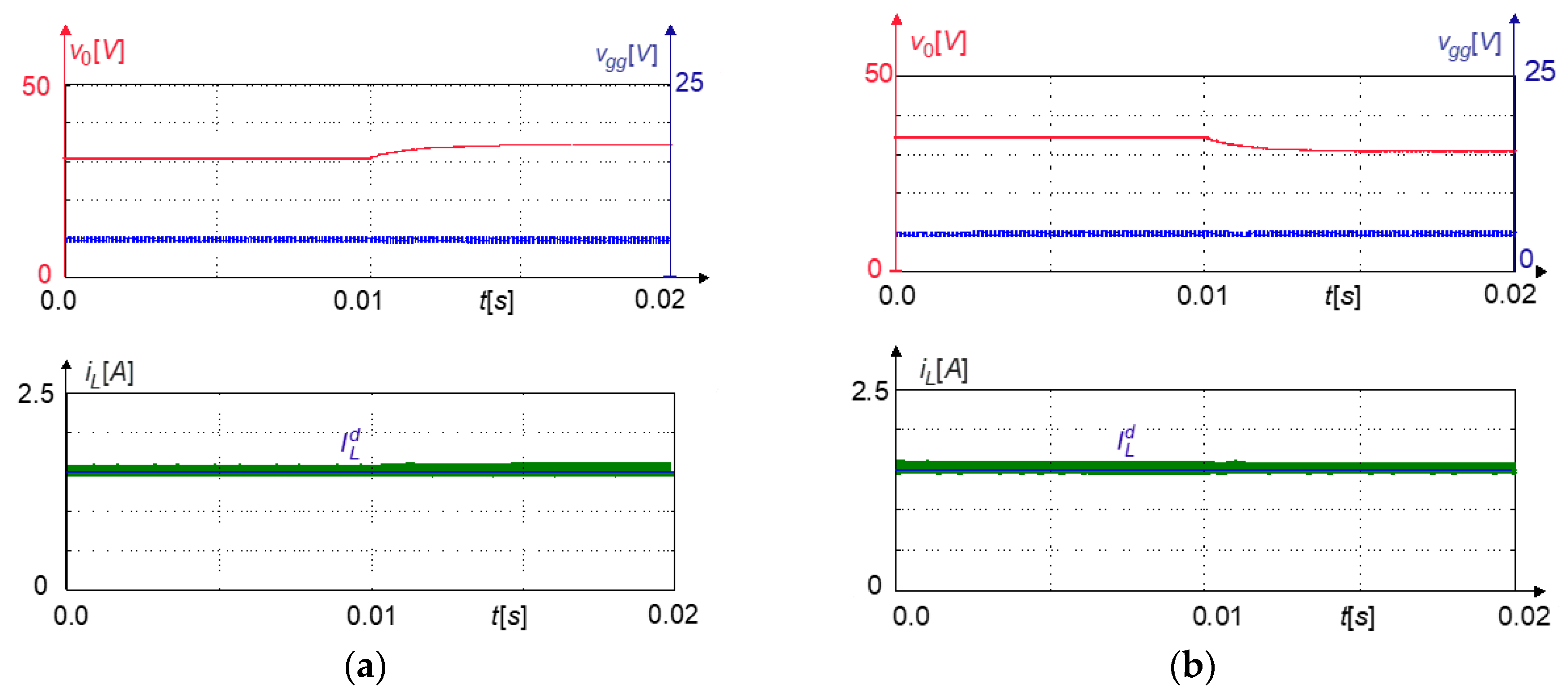
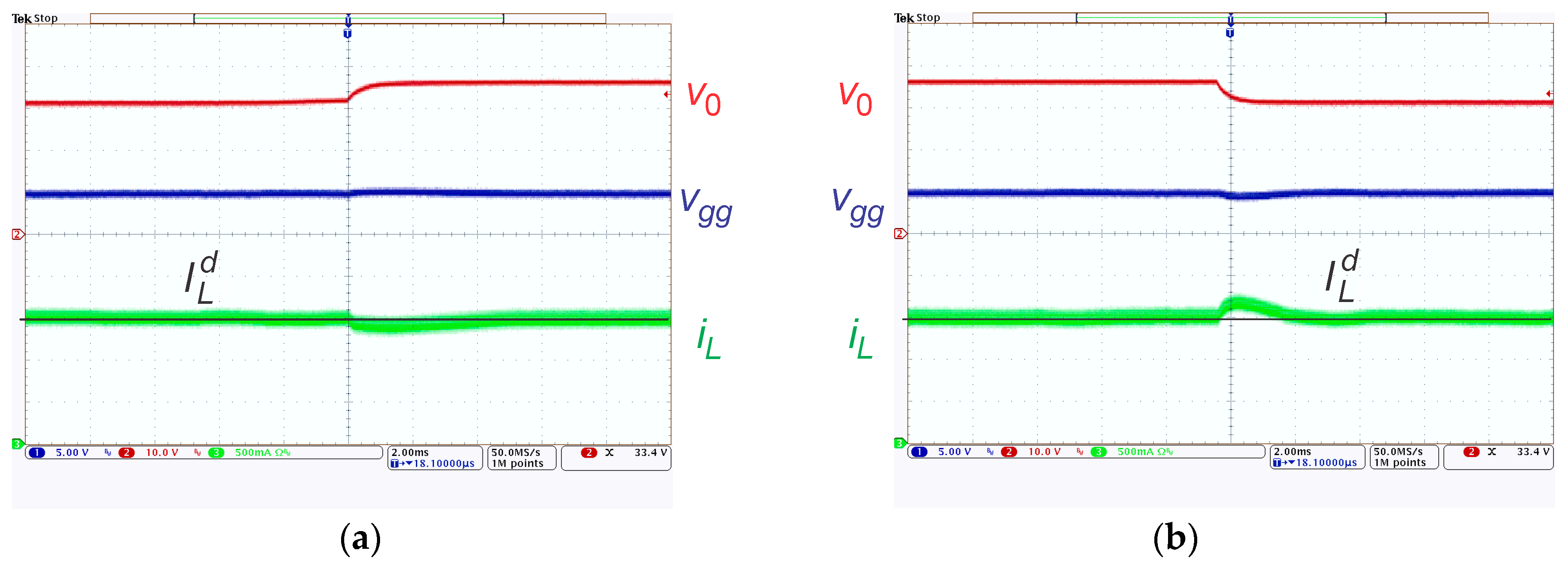
7.2.2. Output Voltage Control

Output voltage control was, as was the case for the current control, demonstrated with the simulations and experiments. Operation with changing reference value of the output voltage is presented in Figure 24 (simulation results) and Figure 25 (experimental results). In Figure 24a, the performance when voltage reference V 0 d was increased from 32 V to 35 V is represented, whereas in Figure 24b, the case when the output voltage reference was reduced from 35 V to 30 V is shown. In Figure 25a the transients when voltage reference V 0 d was changing from 30 V to 35 V, and in Figure 25 the voltage reference V 0 d was changing from 35 V to 30 V. The product ZD was set to the constant value (ZD = 40%), and the load resistance R0 to 80 Ω. TEG open terminal voltage was Vg = 8.65 V.
For both simulation and experimental results, the top graph shows the output voltage v0 (represented in red), its reference value V 0 d (represented in black), the voltage on the SC stage capacitors vCk (represented in pink), and converter input voltage (TEG output voltage) vgg (represented in blue). On the bottom graph for the simulation results, the inductor current is represented in green and its reference value I L d in black. The same presentation (top and bottom graphs) and colour scheme are used for the representation of the same values in the case of the experimental results, with the exception of the reference value of the inductor current, which cannot be represented for the experimental results. This representation, including the colour scheme, was also used in the additional experimental results featured in Figure 26, Figure 27, Figure 28 and Figure 29.
Satisfactory output voltage tracking behaviour can be observed for both simulation and experimental results. The overshoot represented in experimental results for increased desired output voltage can be reduced with the appropriate choice of linear controller parameters. In the case of increased output voltage demand, the converter input voltage drops, together with the voltage on the capacitors in the SC-circuit. A good tracking behaviour can also be observed for the inductor current (controlled in the inner control loop). An overshoot can be observed in the inductor current response, as a result of the overshoot in the output voltage response.
The results show that the operation is not completely symmetrical in terms of the transient when the desired voltage value is increased or decreased. This is due to the fact that the SC-BC is strictly unidirectional, and the increased load demands can be covered for from the source (TEG), whereas in the case of load reduction, the excess energy can only be consumed by the load. This behaviour is evident in both the simulation and experimental results. It is also important to note that, as opposed to the inductor current control, the linearization method is not very precise, as it required for the use of several assumptions and approximations.
The behaviour in the case of the load variation for ZD = 40% is represented in Figure 26 (simulation results) and Figure 27 (experimental results). The reference value of the output voltage was 32 V (30 V for experimental results), and the output resistance R0 was changing from 100 Ω to 80 Ω (Figure 26a and Figure 27a) 80 Ω to 100 Ω (Figure 26b and Figure 27b). It can be observed that the voltage controller rejects the effect of the load variation successfully in both cases. The transient is relatively fast, in the range of 3 ms, and the resulting overshoot is low, in the range of 2 V (at the output voltage set to 30 V this is between 5 and 10%). The current response also exhibits an overshoot; after the transient, the current settles at the higher value in the case of the increased load, and at the lower value in the case of the reduced load. The converter input voltage vgg and the SC-circuit capacitance voltage vCk again show almost exact matching, as expected.
To prove the successful operation of the voltage controlled SC-BC further, additional experimental results are featured in Figure 28 and Figure 29. Figure 28 features the case when the product ZD was set to the higher value (ZD = 50%) and the voltage reference V 0 d was increased from 30 V to 35 V (Figure 28a) and decreased from 35 V to 30 V (Figure 28b). The load resistance R0 is 80 Ω and TEG open terminal voltage was Vg = 8.65 V. A good output voltage tracking with a small overshoot in both output voltage and current can be observed.
To demonstrate the load variation rejection for the duty cycle product ZD set to 50% and the reference value of the output voltage set to 30 V, the experimental results are shown in Figure 29, for the cases when the output resistance R0 was changed from 80 Ω to 100 Ω (Figure 29a) and from 100 Ω to 80 Ω (Figure 29b). After the short transient, the output voltage was kept on the same value it had before the changing of voltage, closely tracking the reference value. The output voltage overshoot was in the range of 2 V with the duration of about 1 ms. The inductor current decreased in the case of the reduced load and increased in the case of increased load, as expected.
Like in the case of the inductor current control, the value of ZD was set to the values 0.4 and 0.5, and the maximal value of D was set to approximately 0.7, as calculated using Equation (22). Thus, again, the performance was represented in the complete operation area. The behaviour of the SC-BC was only shown with the experimental results for ZD = 0.5, because the results do not differ significantly from the ones obtained for ZD = 0.4, which is demonstrated sufficiently with the experimental results.
The stable operation of the control algorithms can be demonstrated with the use of the simulation and experimental results. Within the available limits of the operation, the SC-BC operation was shown to be satisfactory.

8. Discussion

A switched-capacitor boost DC-DC converter to be applied for thermal energy harvesting in PV systems is presented in this paper. When such a converter is applied, additional energy can be obtained from the PV panels, increasing their performance and cost effectiveness. TEGs, placed on the backside of the panel, can be used for the input of the converter, and, in a typical application, the converter is connected in parallel with the main PV converter, operating as a current source. In this case, only current control is required, and, because the value of the converter output current can be calculated easily using the static characteristics of the converter, the control of the inductor current would be sufficient. However, the output voltage control was also developed and evaluated to represent the possibility of a standalone operation and evaluate the full potential of the converter.
The converter is an integration of the switched-capacitor circuit and a boost converter. It can be used in applications where no galvanic isolation is required. The MOSFETs were used as switching elements rather than diodes, because their conducting power losses are lower, and the voltage drop on the MOSFET is significantly lower than the diode forward voltage drop. It has been demonstrated by analytical studies, as well as simulations and experiments, that a voltage gain can be increased significantly, which is of special importance in the case of using TEGs, where the output voltage is relatively low. The efficiency was increased significantly. In the optimal point (Z = 0.8, D = 0.6) the efficiency of 95% was reached, whereas with the use of the diode based converter with the same power rating and passive elements’ values, the maximal efficiency achieved was 79%. The voltage could be increased to achieve an even higher voltage gain by simply adding more capacitor stages in the SC. The converter can operate with relatively low duty cycles.
Additionally, if compared to the other recently published methods, the number of inductors is low, and the MOSFETs used as switches can be integrated. In case of very low power this can also be true for SC capacitors. The values of passive components, BC inductance L, as well as output BC capacitance C0 and SC capacitance Ck, were calculated, and the method of their choice is presented in the paper. Likewise, the limitations of the operating parameters (duty cycle D) of the converter were evaluated and used for the on-line setting of controller limits.
The dynamics of the converter were evaluated, and a dynamic model was created using the state-averaging method. The behaviour of not only inductor current and output voltage, but also the capacitor voltage and current in the switched capacitors’ stage, can be evaluated with the use of this model. Also, the control algorithms for inductor current and output voltage were developed based on this model. Linearization methods were used. The linearised models were controlled by classical linear PI controllers. The dynamics of the converter are highly nonlinear, and the use of only linear controllers would not be sufficient for stable and robust control behaviour. The model-based approach is applied for the linearization, utilising the model obtained by the state space averaging method. This approach enables the operation in a relatively wide area, not only in a single operating point.
The effects of the variation of SC-BC parameters were evaluated, as well as the varying load. It was shown that the control algorithm is not significantly impacted by the parameter mismatches, and the control behaviour remains stable.
To summarise, the main advantages of the SC-BC presented in the paper are:
  • Only one inductor is used and no transformers,
  • MOSFETs are used in place of diodes as switching elements, resulting in low conduction losses,
  • Duty cycles are not overlong,
  • The switching-capacitor stage can be integrated.
On the other hand, in our view, the main disadvantages are the number of switching elements and relatively complex control. The high number of switches can be overcome by the integration, whereas the complex control is becoming an ever smaller problem due to the rapid advance in integrated circuits, microcontrollers and SOCs.
Simulation and experimental results for the 30 W DC-DC converter are included, which verify the proposed converter structure and control approach. In both cases, satisfactory results can be observed regarding the response to the changed desired value of inductor current and output voltage, as well as the varying load.
In future work, the focus will be on the simplification of the control algorithm and extending the operation range by control of the switched capacitor voltage. Robustness to the TEG parameter variations will remain an important issue. MPPT algorithms will be developed for the determination of the most appropriate value of switched capacitors` charging duty cycle z. Using a different, possibly integral, method for the measurement of currents will also be of interest.

Author Contributions

All authors contributed equally to the paper. They developed the converter and control algorithms jointly. They also performed experiments and evaluated results jointly.

Funding

This research received no external funding.

Conflicts of Interest

The authors declare no conflict of interest.

Abbreviations

Acronyms
BSBoost Stage
CCMContinuous Conduction Mode
DCDirect Current
DC-DCDirect Current-Direct Current
DCMDiscontinuous Conduction Mode
ESREquivalent Series Resistance of capacitor
MOSFETMetal-Oxide-Semiconductor Field-Effect Transistor
MPPTMaximum Power Point Tracking
PIProportional-Integral
PVPhotovoltaic
PWMPulse Width Modulation
SCSwitched-Capacitor
SC-BCSwitched-Capacitor-Boost Converter
SOCSystem On Chip
TEGThermoelectric generator
Nomenclature
A v converter static gain
C 0 output capacitance
C 1 , C 2 , C 3 capacitances of switched capacitors
C k capacitance of switched capacitors
dduty-cycle function over the interval T s
Daverage value of duty-cycle function over the interval T s
D m a x maximal value of duty cycle
D m i n minimal value of duty cycle
f s switching frequency of the converter
i i n converter input current
I i n average value of converter input current over the interval T s
i L inductor current
I L average value of inductor current iL over the interval T s
I L ( s ) Laplace transform of I L
i L d desired value of inductor current
I L d average value of desired value of inductor current over the interval T s
I L d ( s ) Laplace transform of i L d
IL,maxmaximal value of inductor current (current ripple)
IL,minminimal value of inductor current (current ripple)
i R 0 output current
I R 0 average value of output current iR0 over the interval T s
I R 0 ( s ) Laplace transform of I R 0
Linductance of the boost stage inductor
R 0 output (load) resistance
r d 1 r d 6 MOSFET drain-source on resistance of transistors T 1 d T 6 d
r d s 1 r d s 5 MOSFET drain-source on resistance of transistors T 1 T 5
R D S ( o n ) MOSFET drain-source on resistance
R g inner TEG resistance
R L resistance of the boost stage inductor
ttime
T s sample time interval
u i L linear feedback inductor current controller output
U i L average value of linear feedback inductor current controller output over the interval T s
U i L ( s ) Laplace transform of U i L
u v 0 linear feedback output voltage controller output
U v 0 average value of linear feedback output voltage controller output over the interval T s
U v 0 ( s ) Laplace transform of U v 0
u v C k linear feedback switched capacitor voltage controller output
U v C k average value of linear feedback switched capacitor voltage controller output over the interval T s
U v C k ( s ) Laplace transform of U v C k
v 0 output voltage
V 0 average value of output voltage over the interval T s
V 0 ( s ) Laplace transform of V 0
v 0 d desired value of the output voltage
V 0 d average value of desired value of the output voltage over the interval T s
V 0 d ( s ) Laplace transform of V 0 d
v0,maxmaximal value of output voltage (voltage ripple)
v0,minminimal value of output voltage (voltage ripple)
v C k switched capacitor voltage
V C k average value of switched capacitor voltage over the interval T s
V C k ( s ) Laplace transform of V C k
v C k d desired value of the switched capacitor voltage
V C k d average value of desired value of the switched capacitor voltage over the interval T s
V C k d ( s ) Laplace transform of V C k d
V D diode forward voltage
v g open terminal TEG voltage
V g average value of open terminal TEG voltage over the interval T s
v g g SC_BC input terminal voltage
V g g SC_BC input terminal voltage over the interval T s
V g g * input of the boost stage of SC-BC, average value over the interval T s
v L inductor voltage
W L energy stored in inductor L
W C k energy stored in capacitor
zswitched capacitors charging duty cycle over the interval T s
Zaverage value of the switched capacitors charging duty cycle over the interval T s
Δ i L inductor current ripple
Δ v 0 output voltage ripple
εmaximal distance between measurement points and theoretical calculated curve

References

  1. Chandrasekar, M.; Suresh, S.; Senthilkumar, T.; Ganesh Karthikeyan, M. Passive cooling of standalone flat PV module with cotton wick structures. Energy Convers. Manag. 2013, 71, 43–50. [Google Scholar] [CrossRef]
  2. Wang, C.; Chen, W.; Shao, S.; Chen, Z.; Zhu, B.; Li, H. Energy management of standalone hybrid PV system. Energy Procedia 2011, 12, 471–479. [Google Scholar] [CrossRef]
  3. Gentle, A.R.; Smith, G.B. Is enhanced radiative cooling of solar cell modules worth pursuing? Sol. Energy Mater. Sol. Cells 2016, 150, 39–42. [Google Scholar] [CrossRef] [Green Version]
  4. Chandrasekar, M.; Senthilkumar, T. Passive thermal regulation of flat PV modules by coupling the mechanisms of evaporative and fin cooling. Heat Mass Transf. 2016, 52, 1381. [Google Scholar] [CrossRef]
  5. Yang, D.; Yin, H. Energy Conversion Efficiency of a Novel Hybrid Solar System for Photovoltaic, Thermoelectric, and Heat Utilization. IEEE Trans. Energy Convers. 2011, 26, 662–670. [Google Scholar] [CrossRef]
  6. Li, G.; Chen, X.; Jin, Y. Analysis of the Primary Constraint Conditions of an Efficient Photovoltaic-Thermoelectric Hybrid System. Energies 2017, 10, 20. [Google Scholar] [CrossRef]
  7. Narducci, D.; Lorenzi, B. Challenges and perspectives in tandem thermoelectric-photovoltaic solar energy conversion. IEEE Trans Nanotechnol. 2016, 15, 348–355. [Google Scholar] [CrossRef]
  8. Petucco, A.; Saggini, S.; Corradini, L.; Mattavelli, P. Analysis of power processing architectures for thermoelectric energy harvesting. IEEE J. Emerg. Sel. Top. Power Electron. 2016, 4, 1036–1049. [Google Scholar] [CrossRef]
  9. Shen, C.-L.; Chen, H.-Y.; Chiu, P.-C. Integrated Three-Voltage-Booster DC-DC Converter to Achieve High Voltage Gain with Leakage-Energy Recycling for PV or Fuel-Cell Power Systems. Energies 2015, 8, 9843–9859. [Google Scholar] [CrossRef] [Green Version]
  10. Wong, Y.-S.; Chen, J.-F.; Liu, K.-B.; Hsieh, Y.-P. A Novel High Step-Up DC-DC Converter with Coupled Inductor and Switched Clamp Capacitor Techniques for Photovoltaic Systems. Energies 2017, 10, 378. [Google Scholar] [CrossRef]
  11. Shen, C.-L.; Chiu, P.-C.; Lee, Y.-C. Novel Interleaved Converter with Extra-High Voltage Gain to Process Low-Voltage Renewable-Energy Generation. Energies 2016, 9, 871. [Google Scholar] [CrossRef]
  12. Leon-Masich, A.; Valderrama-Blavi, H.; Bosque-Moncusí, J.M.; Maixé-Altés, J.; Martínez-Salamero, L. Sliding-Mode-Control-Based Boost Converter for High-Voltage–Low-Power Applications. IEEE Trans. Ind. Electron. 2015, 62, 229–237. [Google Scholar] [CrossRef]
  13. Luo, F.L.; Ye, H. Advanced DC/DC Converters, 2nd ed.; CRC Press: Boca Raton, FL, USA, 2017; ISBN 978-1498774901. [Google Scholar]
  14. Luo, F.L.; Ye, H. Super-lift boost converters. IET Power Electron. 2014, 7, 1655–1664. [Google Scholar] [CrossRef]
  15. Ioinovici, A. Switched-capacitor power electronics circuits. IEEE Circuits Syst. Mag. 2001, 1, 37–42. [Google Scholar] [CrossRef]
  16. Wu, B.; Li, S.; Smedley, K.M.; Singer, S. Analysis of highpower switched capacitor converter regulation based on charge-balance transient-calculation method. IEEE Trans. Power Electron. 2016, 31, 3482–3494. [Google Scholar] [CrossRef]
  17. Maksimovic, D.; Ćuk, S. Switching converters with wide DC conversion range. IEEE Trans. Power Electron. 1991, 6, 151–157. [Google Scholar] [CrossRef] [Green Version]
  18. Wijeratne, D.S.; Moschopoulos, G. Quadratic Power Conversion for Power Electronics: Principles and Circuits. IEEE Trans. Circuits Syst. Regul. Pap. 2012, 59, 426–438. [Google Scholar] [CrossRef]
  19. Loera-Palomo, R.; Morales-Saldana, J.A. Family of quadratic step-up dc–dc converters based on non-cascading structures. IET Power Electron. 2015, 8, 793–801. [Google Scholar] [CrossRef]
  20. Divya Navamani, J.; Vijayakumar, K.; Jegatheesan, R. Non-isolated high gain DC-DC converter by quadratic boost converter and voltage multiplier cell. Ain Shams Eng. J. 2016. [Google Scholar] [CrossRef]
  21. Axelrod, B.; Berkovich, Y.; Ioinovici, A. Switched-Capacitor/Switched-Inductor Structures for Getting Transformerless Hybrid DC–DC PWM Converters. IEEE Trans. Circuits Syst. Regul. Pap. 2008, 55, 687–696. [Google Scholar] [CrossRef]
  22. Tran, V.-T.; Nguyen, M.-K.; Choi, Y.-O.; Cho, G.-B. Switched-Capacitor-Based High Boost DC-DC Converter. Energies 2018, 11, 987. [Google Scholar] [CrossRef]
  23. Nguyen, M.; Duong, T.; Lim, Y. Switched-Capacitor-Based Dual-Switch High-Boost DC–DC Converter. IEEE Trans. Power Electron. 2018, 33, 4181–4189. [Google Scholar] [CrossRef]
  24. Padmanaban, S.; Bhaskar, M.S.; Maroti, P.K.; Blaabjerg, F.; Fedák, V. An Original Transformer and Switched-Capacitor (T & SC)-Based Extension for DC-DC Boost Converter for High-Voltage/Low-Current Renewable Energy Applications: Hardware Implementation of a New T & SC Boost Converter. Energies 2018, 11, 783. [Google Scholar] [CrossRef]
  25. Chen, S.-J.; Yang, S.-P.; Huang, C.-M.; Chou, H.-M.; Shen, M.-J. Interleaved High Step-Up DC-DC Converter Based on Voltage Multiplier Cell and Voltage-Stacking Techniques for Renewable Energy Applications. Energies 2018, 11, 1632. [Google Scholar] [CrossRef]
  26. Abutbul, A.; Gherlitz, A.Y.; Berkovich, Y.; Ioinovici, A. Step-Up Switching-Mode Converter With High Voltage Gain Using a Switched-Capacitor Circuit. IEEE Trans. Circuits Syst. I Fundam. Theory Appl. 2003, 50, 1098–1102. [Google Scholar] [CrossRef]
  27. Maruša, L.; Milanovič, M.; Valderrama-Blavi, H. Evaluating a Switched Capacitor-Boost Converter (SC-BC) for energy harvesting in a Peltier-cells thermoelectric system. In Proceedings of the Electrical Drives and Power Electronics Conference (EDPE), Tatranska Lomnica, Slovakia, 21–23 September 2015. [Google Scholar] [CrossRef]
  28. Slotine, J.J.E.; Li, W. Applied Nonlinear Control; Prantice-Hall: Englewood Cliffs, NJ, USA, 1991; ISBN 978-0130408907. [Google Scholar]
  29. Dodds, S.J. Feedback Control; Advanced Textbooks in Control and Signal Processing; Springer: London, UK, 2015; ISBN 978-1-4471-6674-0. [Google Scholar] [CrossRef]
  30. Mohan, N.; Undeland, T.M.; Robbins, W.P. Power Electronics: Converter, Application and Design, 3rd ed.; John Wiley & Sons: New York, NY, USA, 2007; ISBN 978-8126510900. [Google Scholar]
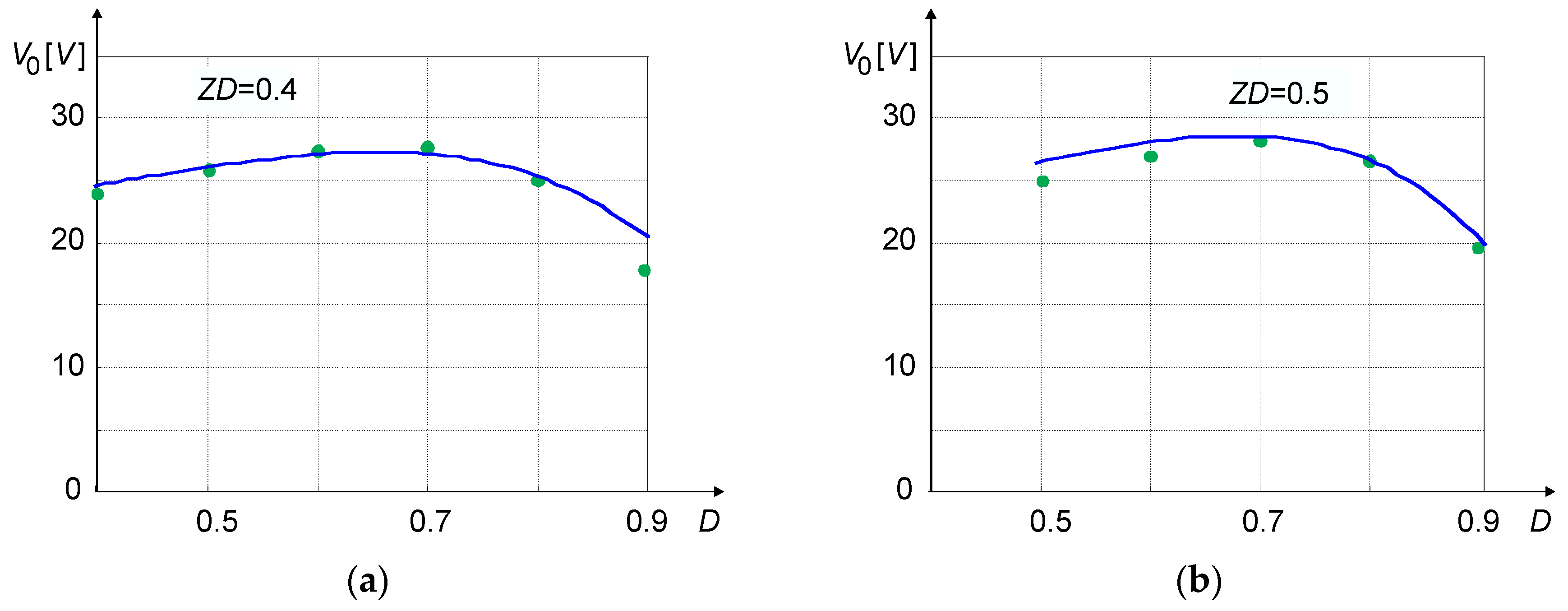
Figure 1. Switched capacitor-boost converter, basic principle; SC-circuit is represented in the red frame and BC in the blue frame.
Energies 11 03156 g001
Figure 2. Switched Capacitor-Boost Converter (SC-BC), the SC-circuit is represented in the red frame and BC in the blue frame: (a) Diode based SC-BC; (b) MOSFET based SC-BC.
Energies 11 03156 g002
Figure 3. Switched-Capacitor-Boost Converter modes of operation: (a) Diode based converter, parallel charging of SC stage capacitors and inductor; (b) MOSFET based converter, parallel charging of SC stage capacitors and inductor; (c) Both variants, charging inductor from SC capacitors in series with voltage source; (d) Both variants, discharging to output.
Energies 11 03156 g003
Figure 4. Switching sequences: (a) Diode based SC-BC; (b) MOSFET based SC-BC.
Energies 11 03156 g004
Figure 5. Dynamic model of the MOSFET based SC-BC.
Energies 11 03156 g005
Figure 6. Calculated output voltages of SC-BC: (a) For diode based circuit V0 = f(D,ZD) (Vg = 8.6 V, VD = 0.8 V); (b) For MOSFET based circuit V0 = f(D,ZD) (Vg = 8.6 V, VD = 0.0 V).
Energies 11 03156 g006
Figure 7. SC-BC operation: (a) Calculated input terminal voltages of SC-BC; (b) Calculated gain characteristics for MOSFET based circuit Av = f(D,ZD); where VD = 0.
Energies 11 03156 g007
Figure 8. Switching sequences for current and voltage ripple, necessary for design of passive elements.
Energies 11 03156 g008
Figure 9. Control scheme: (a) Basic principle of the SC-BC control; (b) Basic principle of the SC-BC control when constant value of ZD is used.
Energies 11 03156 g009
Figure 10. Control of inductor current—block scheme (converter model—black; control algorithm—red).
Energies 11 03156 g010
Figure 11. Control of output voltage—block scheme (converter model—black; control algorithm—red).
Energies 11 03156 g011
Figure 12. Control scheme—detailed graphical representation; constant value of ZD is used.
Energies 11 03156 g012
Figure 13. Experimental setup.
Energies 11 03156 g013
Figure 14. Calculated output voltage V0 of SC-BC—static characteristics (function of ZD and D); shaded area is used for verification purposes.
Energies 11 03156 g014
Figure 15. Static characteristics of output voltage V0; green dots (measured) and blue curve (calculated): (a) V0 = f(D) when ZD = 0.4; (b) V0 = f(D) when ZD = 0.5.
Energies 11 03156 g015
Figure 16. Simulation results, current control, transients when ZD = 40%, R0 = 70 Ω and reference current changes: (a) From 1.0 A to 1.8 A; (b) From 1.8 A to 1.0 A.
Energies 11 03156 g016
Figure 17. Experimental results, current control, transients when ZD = 40%, R0 = 80 Ω and reference current changes: (a) From 1.0 A to 1.8 A; (b) From 1.8 A to 1.0 A; x-axis 2 ms/div, y-axis; v0-10 V/div, vgg-5 V/div, iL-500 mA/div.
Energies 11 03156 g017
Figure 18. Simulation results, current control, ZD = 40% and current reference is set to I L d = 1.2 A, transients when output resistance R0 was changed from: (a) 60 Ω to 80 Ω; (b) 80 Ω to 60 Ω.
Energies 11 03156 g018
Figure 19. Experimental results, current control, ZD = 40% and current reference is set to I L d = 1.2 A, transients when output resistance R0 was changed from: (a) 60 Ω to 80 Ω; (b) 80 Ω to 60 Ω; where x-axis 2 ms/div, y-axis; v0-10 V/div, vgg-5 V/div, iL-500 mA/div.
Energies 11 03156 g019
Figure 20. Simulation results, current control, transients when ZD = 50%, R0 = 70 Ω and reference current changes from: (a) 1.4 A to 2.0 A; (b) 1.8 A to 1.0 A.
Energies 11 03156 g020
Figure 21. Experimental results, current control, transients when ZD = 50%, R0 = 60 Ω and reference current changes from: (a) 1.4 A to 2.0 A; (b) 1.8 A to 1.0 A; where x-axis 2 ms/div, y-axis; v0-10 V/div, vgg-5 V/div, iL-500 mA/div.
Energies 11 03156 g021
Figure 22. Simulation results, current control, ZD = 50% and current reference is set to I L d = 1.5 A, transients when output resistance R0 was changed from: (a) 70 Ω to 80 Ω; (b) 80 Ω to 70 Ω.
Energies 11 03156 g022
Figure 23. Experimental results, current control, ZD = 50% and current reference is set to I L d = 1.5 A, transients when output resistance R0 was changed from: (a) 70 Ω to 80 Ω; (b) 80 Ω to 70 Ω; where x-axis 2 ms/div, y-axis; v0-10V/div, vgg-5 V/div, iL-500 mA/div.
Energies 11 03156 g023
Figure 24. Simulation results, voltage control when ZD = 40%, R0 = 80 Ω and transients when voltage reference V 0 d was changing from: (a) 32 V to 35 V; (b) 35 V to 30 V.
Energies 11 03156 g024
Figure 25. Experimental results, voltage control when ZD = 40%, R0 = 80 Ω and transients when voltage reference V 0 d was changing from: (a) 30 V to 35 V; (b) 35 V to 30 V; where x-axis 1 ms/div, y-axis; v0-10 V/div, vgg-5 V/div, vCk-5 V/div iL-500 mA/div.
Energies 11 03156 g025
Figure 26. Simulation results, voltage control when ZD = 40%, V 0 d = 32 V, transients when output resistance R0 was changing from: (a) 100 Ω to 80 Ω; (b) 80 Ω to 100 Ω.
Energies 11 03156 g026
Figure 27. Experimental results, voltage control when ZD = 40% and voltage reference was set to V 0 d = 30 V, transients when output resistance R0 was changed from: (a) 80 Ω to 100 Ω; (b) 100 Ω to 80 Ω; where x-axis 1 ms/div, y-axis; v0-5 V/div, vgg-2.5 V/div, vCk-2 V/div iL-250 mA/div.
Energies 11 03156 g027
Figure 28. Experimental results, voltage control when ZD = 50%, R0 = 80 Ω; transients when voltage reference V 0 d was changing from: (a) 30 V to 35 V; (b) 35 V to 30 V; where x-axis 1 ms/div, y-axis; v0-5 V/div, vgg-2.5 V/div, vCk-2 V/div iL-250 mA/div.
Energies 11 03156 g028
Figure 29. Experimental results, voltage control when ZD = 50% and voltage reference was set to V 0 d = 30 V, transients when output resistance R0 was changed from: (a) 80 Ω to 100 Ω; (b) 100 Ω to 80 Ω; where x-axis 2 ms/div, y-axis; v0-5 V/div, vgg-2.5 V/div, vCk-2 V/div iL-250 mA/div.
Energies 11 03156 g029
Table 1. Measurement results.
ZD = 0.4ZD = 0.5
DV0 (V)V0 (V)
0.4024.00-
0.5025.9024.90
0.6027.4726.93
0.7027.7528.20
0.8025.1026.55
0.9017.8219.60

