Design of Reconfigurable Time-to-Digital Converter Based on Cascaded Time Interpolators for Electrical Impedance Spectroscopy †

 , ,
, ,  ,
,
Abstract
1. Introduction
2. Background and Design Specifications
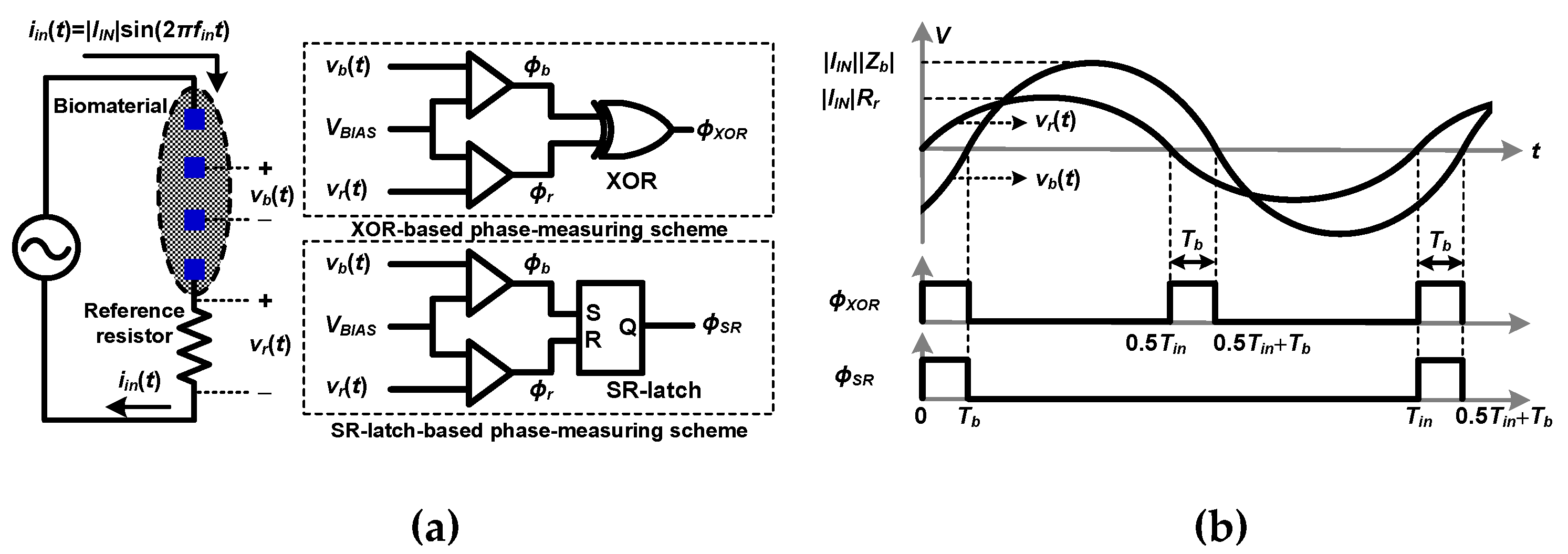
2.1. Impedance Measurement Principle
2.2. Phase Measurement Scheme in Polar Demodulators
2.3. Design Specifications
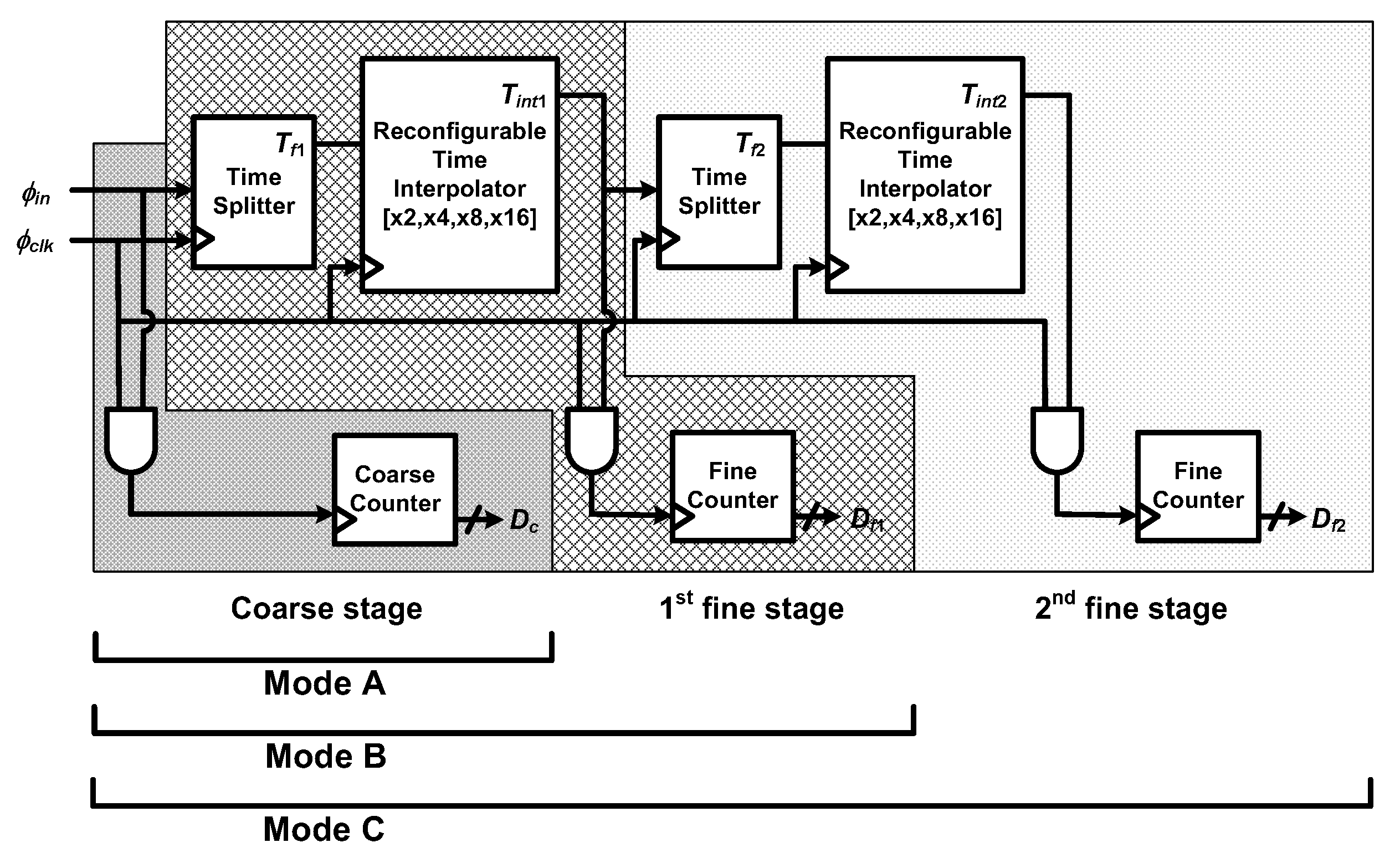
3. Architecture of the Proposed TDC
3.1. Overall Architecture and Operation
3.2. Operation in Mode A
3.3. Operation in Mode B
3.4. Operation in Mode C
4. Circuit Design
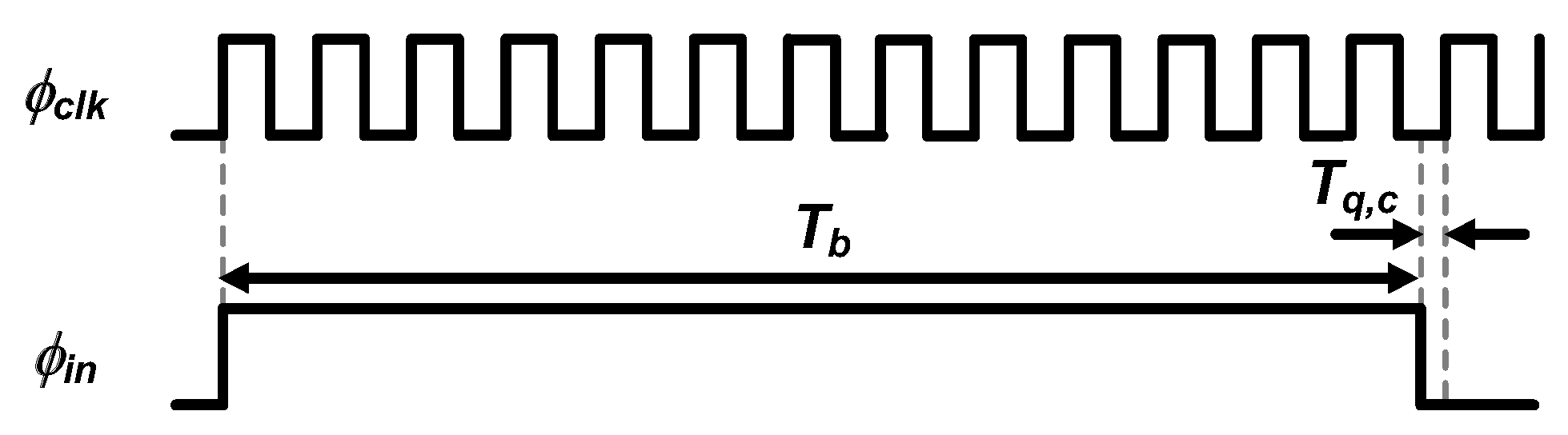
4.1. Time Splitter
4.2. Reconfigurable Time Interpolator
4.3. Novel Features of the Proposed TDC
5. Measurement Results
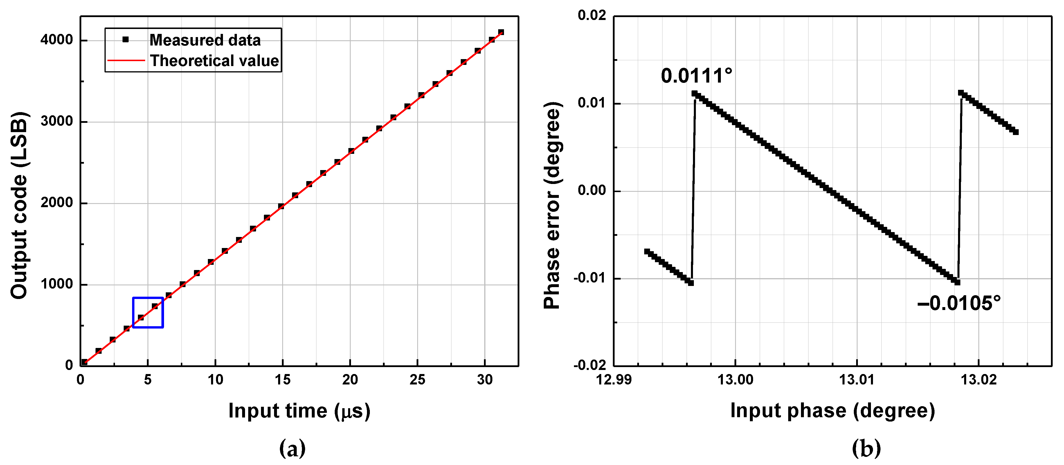
5.1. Mode A
5.2. Mode B
5.3. Mode C
5.4. Error Analysis
5.5. Performance Summary and Comparison
6. Conclusions
Author Contributions
Funding
Acknowledgments
Conflicts of Interest
References
- Choi, A.; Kim, J.Y.; Jo, S.; Jee, J.H.; Heymsfield, S.B.; Bhagat, Y.A.; Kim, I.; Cho, J. Smartphone-based bioelectrical impedance analysis devices for daily obesity management. Sensors 2015, 15, 22151–22166. [Google Scholar] [CrossRef] [PubMed]
- Shin, S.-C.; Lee, J.; Choe, S.; Yang, H.I.; Min, J.; Ahn, K.-Y.; Jeon, J.Y.; Kang, H.-G. Dry electrode-based body fat estimation system with anthropometric data for use in a wearable device. Sensors 2019, 19, 2177. [Google Scholar] [CrossRef] [PubMed]
- Ferreira, J.; Pau, I.; Lindecrantz, K.; Seoane, F. A handheld and textile-enabled bioimpedance system for ubiquitous body composition analysis. An initial functional validation. IEEE J. Biomed. Health Informat. 2017, 21, 1224–1232. [Google Scholar] [CrossRef] [PubMed]
- Halter, R.J.; Hartov, A.; Heaney, J.A.; Paulsen, K.D.; Schned, A.R. Electrical impedance spectroscopy of the human prostate. IEEE Trans. Biomed. Eng. 2007, 54, 1321–1327. [Google Scholar] [CrossRef] [PubMed]
- Åberg, P.; Nicander, I.; Hansson, J.; Geladi, P.; Holmgren, U.; Ollmar, S. Skin cancer identification using multifrequency electrical impedance–a potential screening tool. IEEE Trans. Biomed. Eng. 2004, 51, 2097–2102. [Google Scholar] [CrossRef] [PubMed]
- Kerner, T.E.; Paulsen, K.D.; Hartov, A.; Soho, S.K.; Poplack, S.P. Electrical impedance spectroscopy of the breast: Clinical imaging results in 26 subjects. IEEE Trans. Med. Imag. 2002, 21, 638–645. [Google Scholar] [CrossRef] [PubMed]
- Nyrén, M.; Kuzmina, N.; Emtestam, L. Electrical impedance as a potential tool to distinguish between allergic and irritant contact dermatitis. J. Am. Acad. Dermatol. 2003, 48, 394–400. [Google Scholar] [CrossRef] [PubMed]
- Dean, D.A.; Ramanathan, T.; Machado, D.; Sundararajan, R. Electrical impedance spectroscopy study of biological tissues. J. Electrostat. 2008, 66, 165–177. [Google Scholar] [CrossRef] [PubMed]
- Wei, C.-L.; Wang, Y.-W.; Liu, B.-D. Wide-range filter-based sinusoidal wave synthesizer for electrochemical impedance spectroscopy measurements. IEEE Trans. Biomed. Circuits Syst. 2014, 8, 442–450. [Google Scholar]
- Kweon, S.-J.; Park, J.-H.; Shin, S.-H.; Yoo, H.-J. A low-power polar demodulator for impedance spectroscopy based on a novel sampling scheme. In Proceedings of the 2015 International SoC Design Conference (ISOCC), Gyungju, South Korea, 3–7 November 2015; pp. 331–332. [Google Scholar]
- Kweon, S.-J.; Shin, S.; Park, J.-H.; Suh, J.-H.; Yoo, H.-J. A CMOS low-power polar demodulator for electrical bioimpedance spectroscopy using adaptive self-sampling schemes. In Proceedings of the 2016 IEEE Biomedical Circuits and Systems Conference (BioCAS), Shanghai, China, 17–19 October 2013; pp. 284–287. [Google Scholar]
- Manickam, A.; Chevalier, A.; McDermott, M.; Ellington, A.D.; Hassibi, A. A CMOS electrochemical impedance spectroscopy (EIS) biosensor array. IEEE Trans. Biomed. Circuits Syst. 2010, 4, 379–390. [Google Scholar] [CrossRef] [PubMed]
- Hong, S.; Lee, K.; Ha, U.; Kim, H.; Lee, Y.; Kim, Y.; Yoo, H. A 4.9 mΩ-sensitivity mobile electrical impedance tomography IC for early breast-cancer detection system. IEEE J. Solid-State Circuits 2015, 50, 245–257. [Google Scholar] [CrossRef]
- Li, H.; Liu, X.; Li, L.; Mu, X.; Genov, R.; Mason, A.J. CMOS electrochemical instrumentation for biosensor microsystems: A review. Sensors 2017, 17, 74. [Google Scholar] [CrossRef] [PubMed]
- Kassanos, P.; Triantis, I.F.; Demosthenous, A. A CMOS magnitude/phase measurement chip for impedance spectroscopy. IEEE Sens. J. 2013, 13, 2229–2236. [Google Scholar] [CrossRef]
- Ramos, J.; Ausín, J.L.; Torelli, G. A 1-MHz analog front-end for a wireless bioelectrical impedance sensor. In Proceedings of the 6th Conference on Ph.D. Research in Microelectronics Electronics, Berlin, Germany, 18–21 July 2010; pp. 1–4. [Google Scholar]
- Huang, H.; Palermo, S. A TDC-based front-end for rapid impedance spectroscopy. In Proceedings of the 2013 IEEE 56th International Midwest Symposium on Circuits and Systems (MWSCAS), Columbus, OH, USA, 4–7 August 2013; pp. 169–172. [Google Scholar]
- Shin, S.; Kweon, S.-J.; Park, J.-H.; Choi, Y.-C.; Yoo, H.-J. An efficient, wide range time-to-digital converter using cascaded time-interpolation stages for electrical impedance spectroscopy. In Proceedings of the 2016 IEEE Asia Pacific Conference on Circuits and Systems (APCCAS), Jeju, South Korea, 25–28 October 2016; pp. 425–428. [Google Scholar]
- Kweon, S.-J.; Park, J.-H.; Shin, S.; Yoo, S.-S.; Yoo, H.-J. A reconfigurable time-to-digital converter based on time stretcher and chain-delay-line for electrical bioimpedance spectroscopy. In Proceedings of the 2017 IEEE 60th International Midwest Symposium on Circuits and Systems (MWSCAS), Boston, MA, USA, 6–9 August 2017; pp. 1037–1040. [Google Scholar]
- Chen, P.; Chen, C.-C.; Shen, Y.-S. A low-cost low-power CMOS time-to-digital converter based on pulse stretching. IEEE Trans. Nucl. Sci. 2006, 53, 2215–2220. [Google Scholar] [CrossRef]
- Milovanovic, V.; Zimmermann, H. Analyses of single-stage complementary self-biased CMOS differential amplifiers. In Proceedings of the NORCHIP 2012, Cpenhagen, Denmark, 12–13 November 2012. [Google Scholar]
- Tan, M.-T.; Chang, J.S.; Tong, Y.-C. A process-independent threshold voltage inverter-comparator for pulse width modulation applications. In Proceedings of the 6th IEEE International Conference on Electronics, Circuits and Systems, Pafos, Cyprus, 5–8 September 1999; pp. 1201–1204. [Google Scholar]
- Allen, P.E.; Holberg, D.R. CMOS Analog Circuit Design, 2nd ed.; Oxford University Press: New York, NY, USA, 2002. [Google Scholar]
- Kim, J.; Maitra, R.; Pedrotti, K.D.; Dunbar, W.B. A patch-clamp ASIC for nanopore-based DNA analysis. IEEE Trans. Biomed. Circuits Syst. 2013, 7, 285–295. [Google Scholar] [CrossRef] [PubMed]


| Parameter | Target Level |
|---|---|
| Application | EIS for biomedical applications |
| Range of the injected signal frequency (fin) | 1 kHz to 2.048 MHz |
| Corresponding input-time range for 0° to 90° | 0–122 ns (fin = 2.048 MHz) to 0–250 μs (fin = 1 kHz) |
| Phase resolution | >10 bit |
| Maximum phase error | 1° |
| Corresponding time error | <~1.35 ns (fin = 2.048 MHz), <~2.8 μs (fin = 1 kHz) |
| Reference clock frequency (fclk) | 32.768 MHz |
| Mode | fin (Hz) | 0° to 90° | fclk (Hz) | Coarse | AT1 | AT2 |
|---|---|---|---|---|---|---|
| C | 2.048M | 0~0.1221 μs | 32.768M | 2 bit | 16 | 16 |
| 1.024M | 0~0.2441 μs | 32.768M | 3 bit | 16 | 16 | |
| 512k | 0~0.4883 μs | 32.768M | 4 bit | 16 | 16 | |
| 256k | 0~0.9766 μs | 32.768M | 5 bit | 16 | 8 | |
| 128k | 0~1.9531 μs | 32.768M | 6 bit | 16 | 4 | |
| 64k | 0~3.9063 μs | 32.768M | 7 bit | 16 | 2 | |
| B | 32k | 0~7.8125 μs | 32.768M | 8 bit | 16 | N/A |
| 16k | 0~15.625 μs | 32.768M | 9 bit | 8 | N/A | |
| 8k | 0~31.25 μs | 32.768M | 10 bit | 4 | N/A | |
| 4k | 0~62.5 μs | 32.768M | 11 bit | 2 | N/A | |
| A | 2k | 0~125 μs | 32.768M | 12 bit | N/A | N/A |
| 1k | 0~250 μs | 16.384M | 12 bit | N/A | N/A |
| AT | Nf | EA | EP | EC | EA·EP·EC |
|---|---|---|---|---|---|
| 256 | 2 | 7.6 | 8 | 0.5 | 30.4 |
| 256 | 4 | 12.9 | 16 | 0.25 | 51.6 |
| 256 | 8 | 10.7 | 16 | 0.125 | 21.4 |
| fin (Hz) | AT1 | AT2 | Target Phase Error (°) | Peak-to-Peak Phase Error (°) | Corresponding Time Error (ns) |
|---|---|---|---|---|---|
| 64k | 16 | 2 | 0.022 | 0.037 | 1.61 |
| 128k | 16 | 4 | 0.022 | 0.049 | 1.06 |
| 256k | 16 | 8 | 0.022 | 0.178 | 1.93 |
| 512k | 16 | 16 | 0.022 | 0.721 | 3.91 |
| 1.024M | 16 | 16 | 0.088 | 1.194 | 3.29 |
| 2.048M | 16 | 16 | 0.088 | 2.696 | 3.66 |
| This Work | IEEE Sensors J.’ 2013 [15] | IEEE MWSCAS’ 2013 [17] | IEEE TNS.’ 2006 [20] | IEEE MWSCAS’ 2017 [19] | |
|---|---|---|---|---|---|
| Tech. | 0.25 μm | 0.35 μm | 0.35 μm | 0.35 μm | 0.18 μm |
| Application | EIS | EIS | EIS | N/A | EIS |
| Implementation scope | TDC | Polar demodulator | Polar demodulator | TDC | TDC |
| Architecture | Counter + Cascaded time interpolator | TVC with ADC | Counter | Counter + time stretchers | Counter+ time stretcher + chain-delay-line |
| fin | 1 kHz– 2.048 MHz | 0.1 kHz– 100 kHz | 0.1 kHz– 10 MHz | N/A | 1 kHz– 2.048 MHz |
| fclk | 32.768 MHz | No use | 3.33 GHz | 80 MHz | 32.768 MHz |
| Power | 7.5 mW | 21 mW | *28 mW | 0.75 mW | 2.4 mW |
| Supply | 2.5 V | 2.5 V | 1.8 V | 3 V–4 V | 1.8 V |
| Area | 0.41 mm2 | *0.40 mm2 | *0.40 mm2 | 0.23 mm2 | 0.35 mm2 |
| Time resolution | N/A | N/A | 300 ps | 50 ps | 103 ps–244 ns |
| Phase error | <0.72° (@512 kHz) <2.70° (@2.048 MHz) | <3.95° | <2.2° | N/A | <0.088° |
| Remarks | Meas. | Meas. | Meas. | Meas. | Sim. |
© 2020 by the authors. Licensee MDPI, Basel, Switzerland. This article is an open access article distributed under the terms and conditions of the Creative Commons Attribution (CC BY) license (http://creativecommons.org/licenses/by/4.0/).
Share and Cite
Shin, S.; Jung, Y.; Kweon, S.-J.; Lee, E.; Park, J.-H.; Kim, J.; Yoo, H.-J.; Je, M. Design of Reconfigurable Time-to-Digital Converter Based on Cascaded Time Interpolators for Electrical Impedance Spectroscopy. Sensors 2020, 20, 1889. https://doi.org/10.3390/s20071889
Shin S, Jung Y, Kweon S-J, Lee E, Park J-H, Kim J, Yoo H-J, Je M. Design of Reconfigurable Time-to-Digital Converter Based on Cascaded Time Interpolators for Electrical Impedance Spectroscopy. Sensors. 2020; 20(7):1889. https://doi.org/10.3390/s20071889
Chicago/Turabian StyleShin, Sounghun, Yoontae Jung, Soon-Jae Kweon, Eunseok Lee, Jeong-Ho Park, Jinuk Kim, Hyung-Joun Yoo, and Minkyu Je. 2020. "Design of Reconfigurable Time-to-Digital Converter Based on Cascaded Time Interpolators for Electrical Impedance Spectroscopy" Sensors 20, no. 7: 1889. https://doi.org/10.3390/s20071889
APA StyleShin, S., Jung, Y., Kweon, S.-J., Lee, E., Park, J.-H., Kim, J., Yoo, H.-J., & Je, M. (2020). Design of Reconfigurable Time-to-Digital Converter Based on Cascaded Time Interpolators for Electrical Impedance Spectroscopy. Sensors, 20(7), 1889. https://doi.org/10.3390/s20071889