Long Slender Piezo-Resistive Silicon Microprobes for Fast Measurements of Roughness and Mechanical Properties inside Micro-Holes with Diameters below 100 µm

 , , ,
, , ,  , ,
, ,
Abstract
1. Introduction
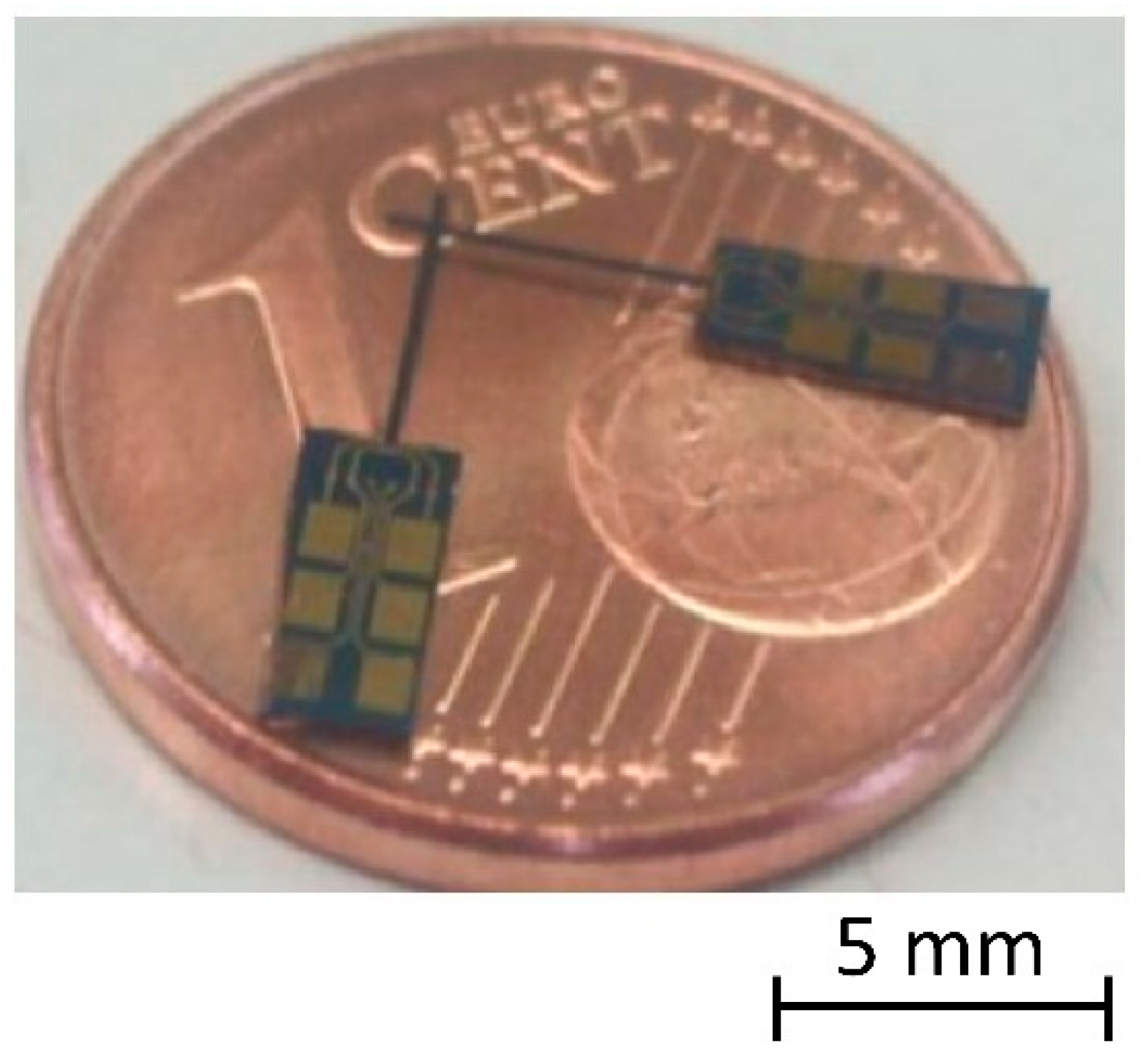
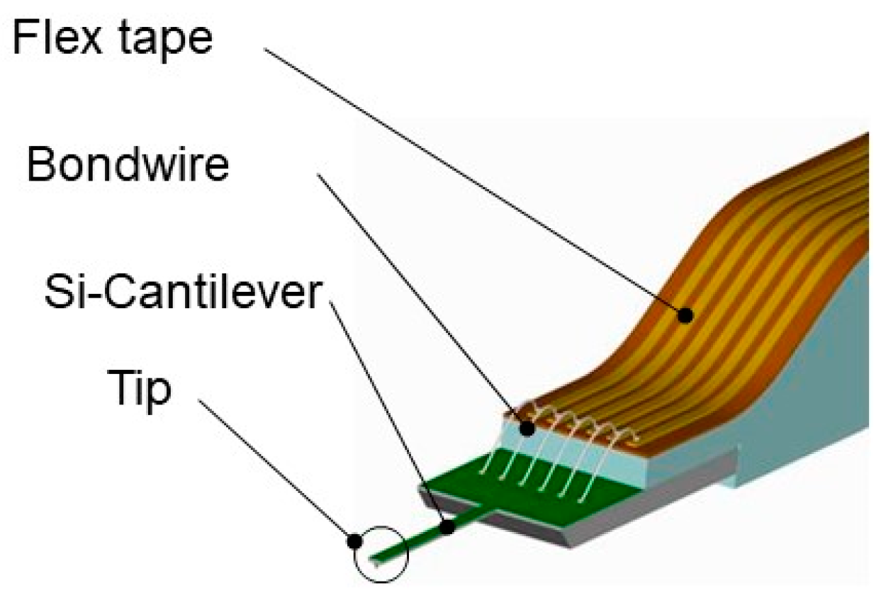
2. Metrological Properties of Piezo-Resistive Silicon Microprobes
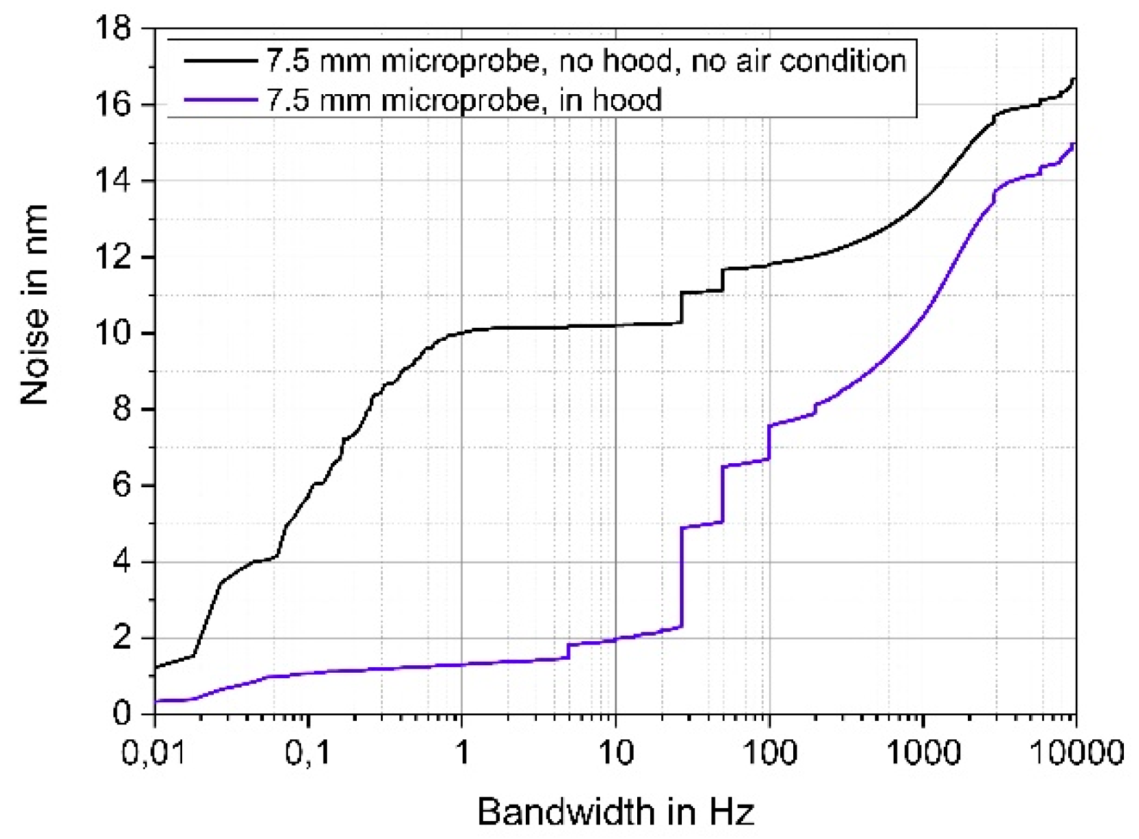
2.1. Noise
2.1.1. Static Microprobe Noise
2.1.2. Static Noise of Microprobe on Measuring Machine Profilescanner
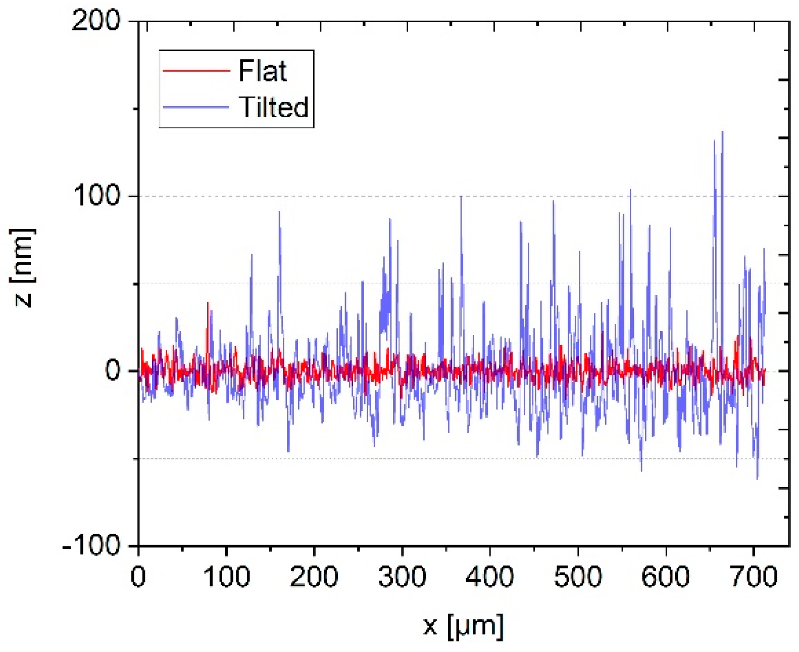
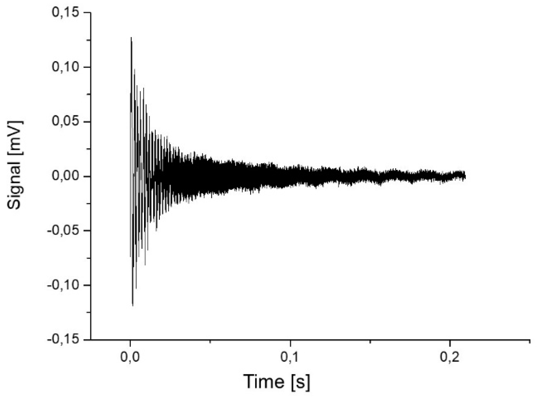
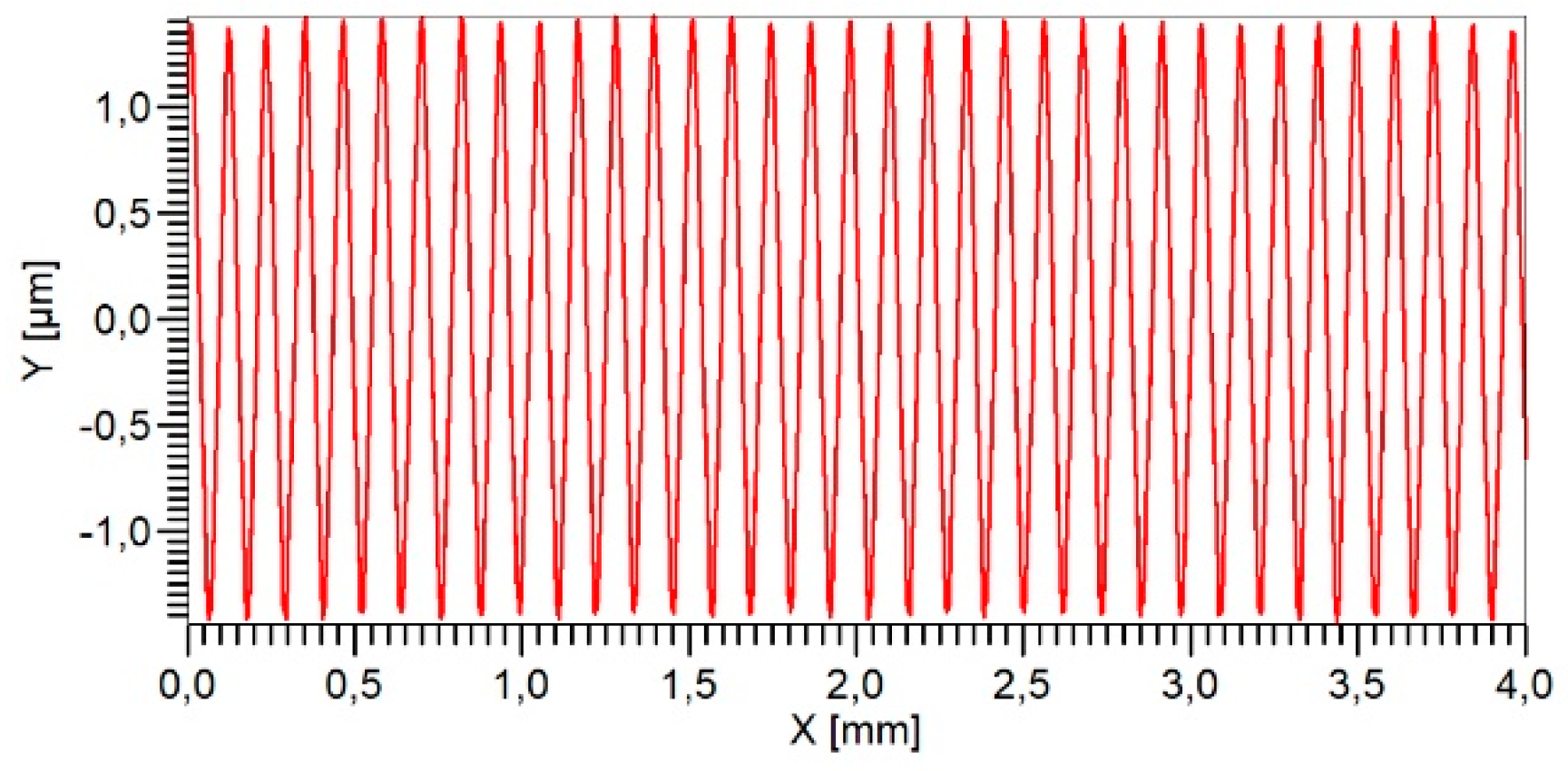
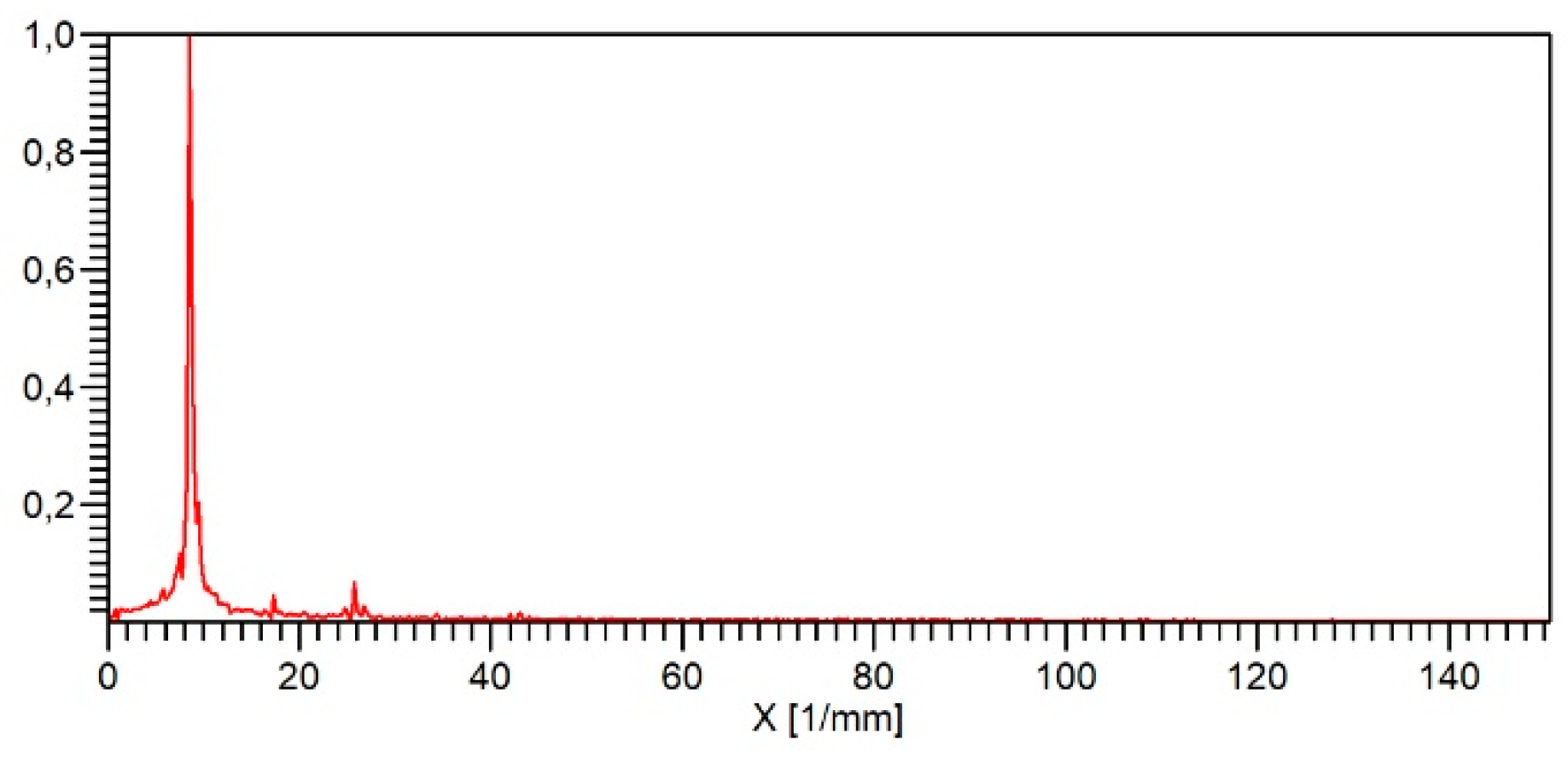
2.1.3. Dynamic Noise of Microprobe for Measuring an Optical Flat
2.1.4. Dynamic Noise of Microprobe for Measuring a Roughness Standard
2.2. Damping
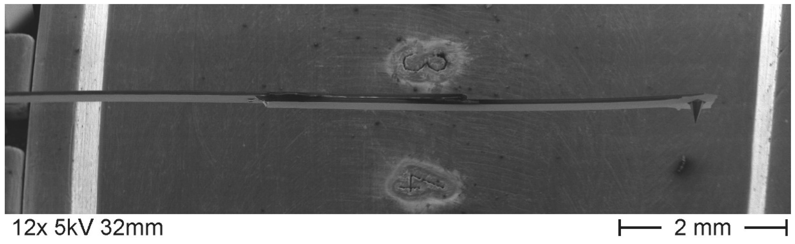
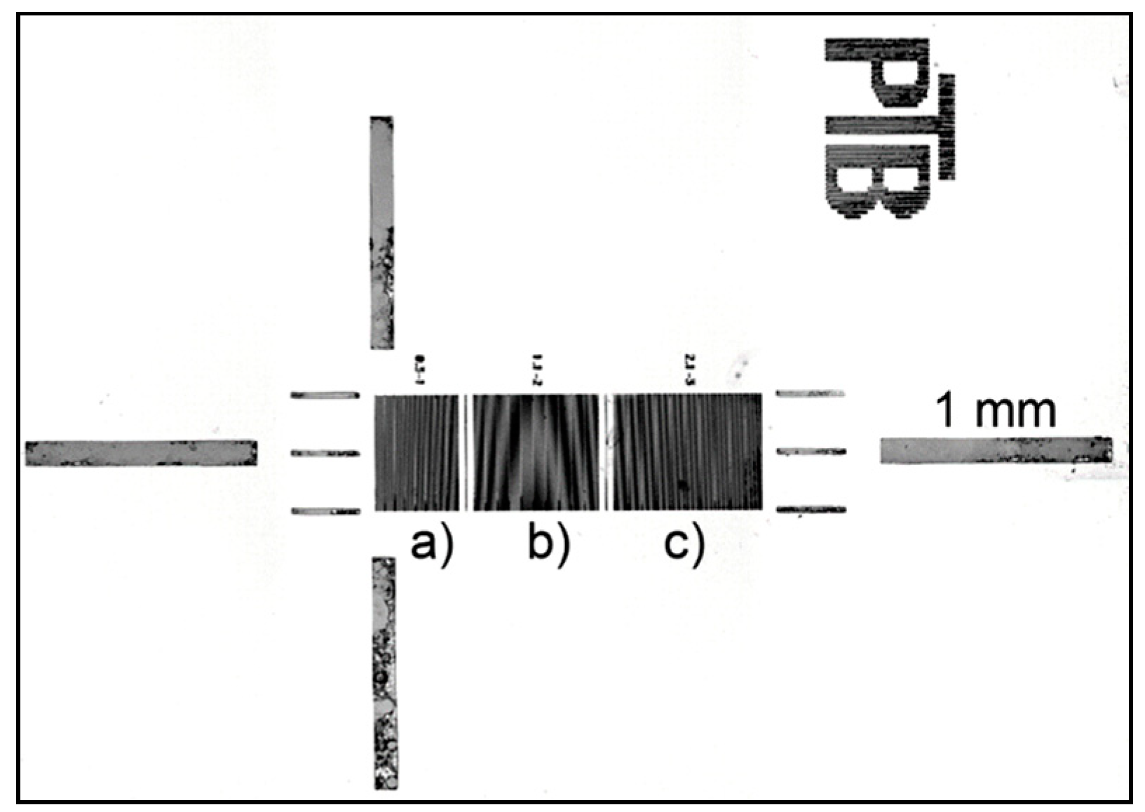
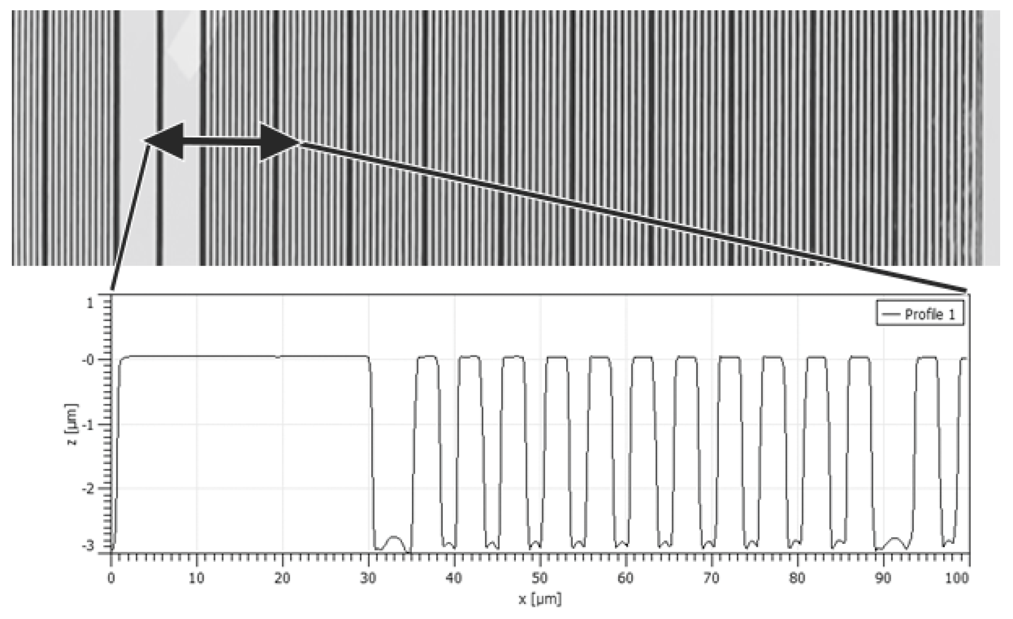
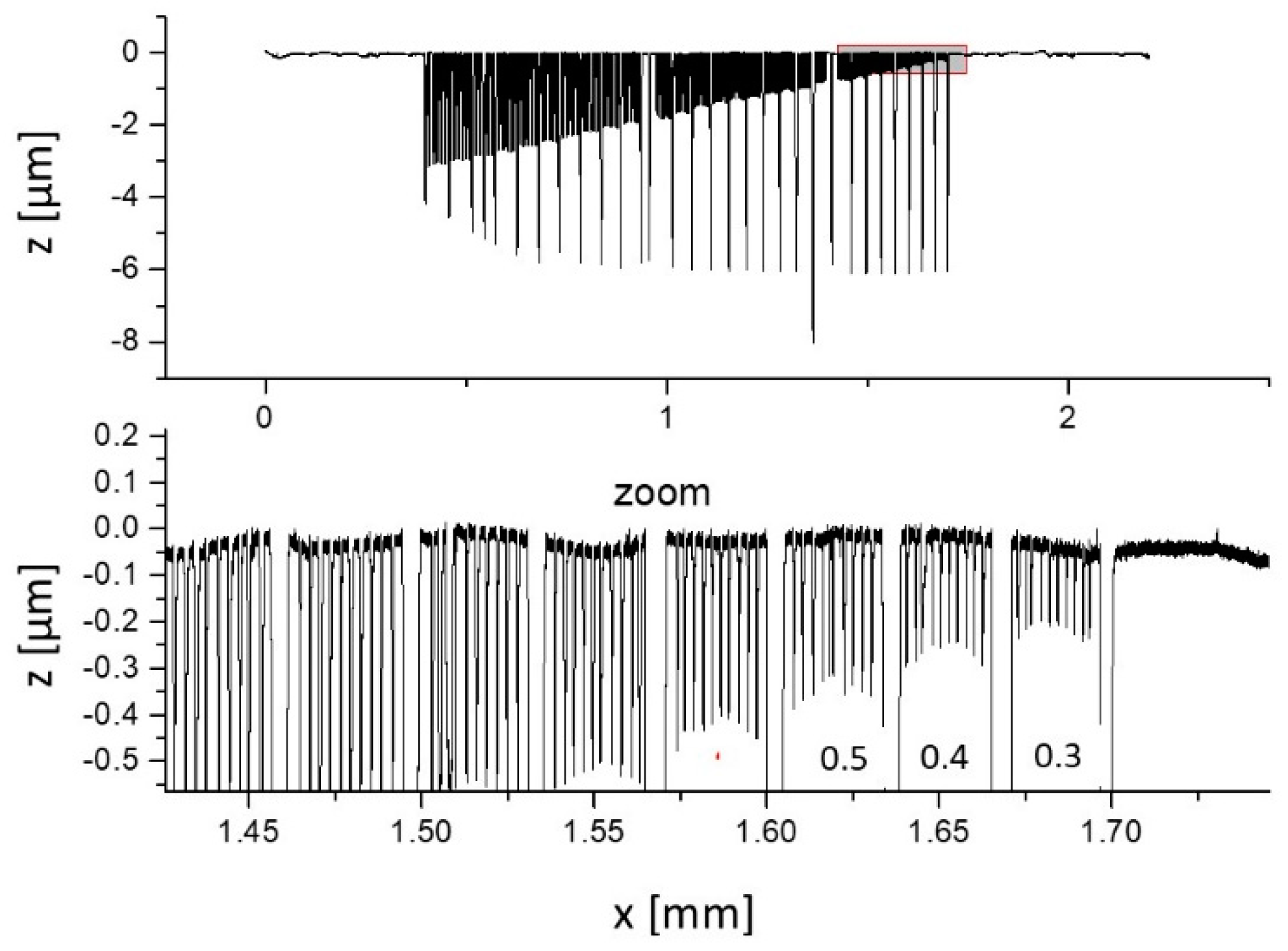
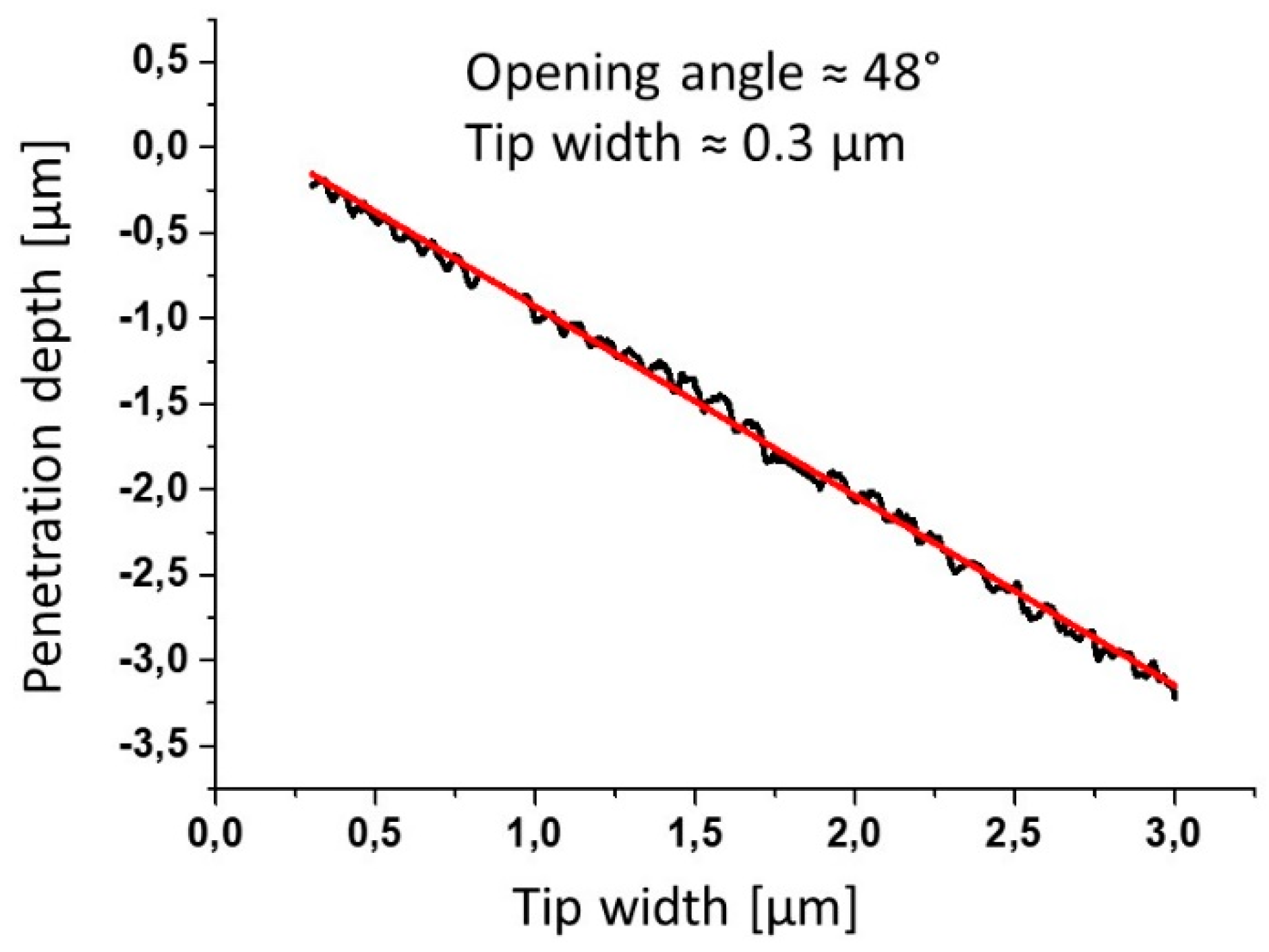
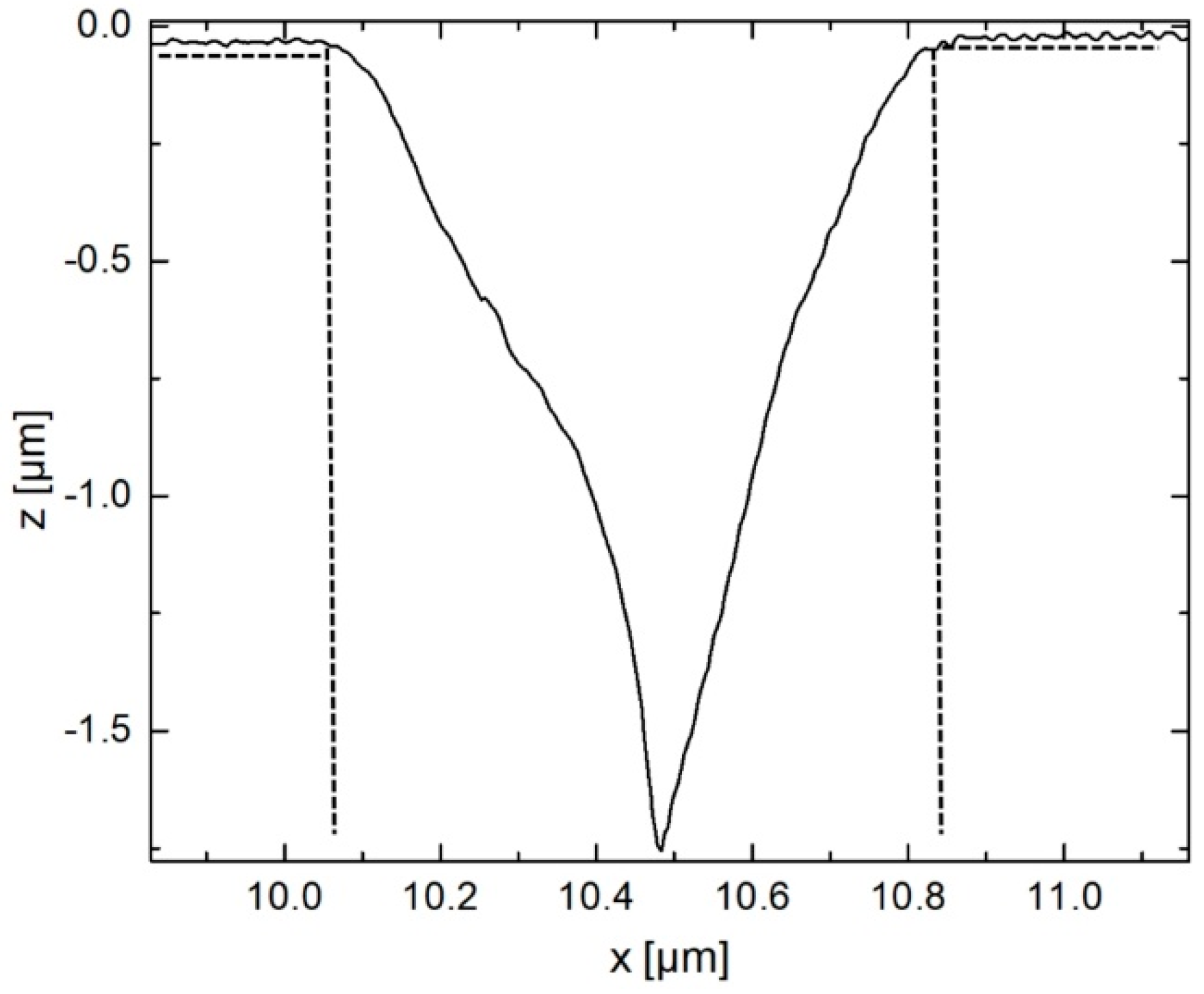
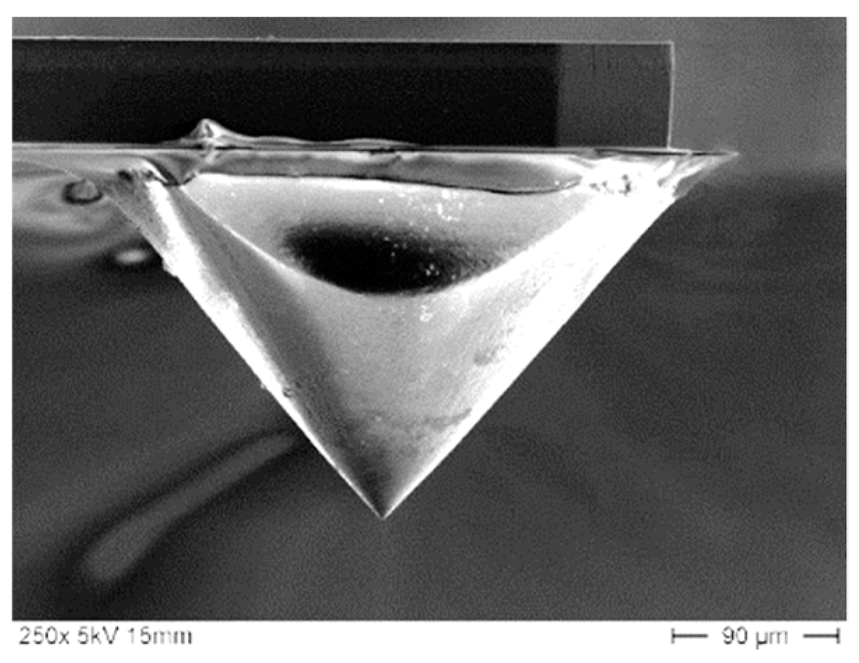
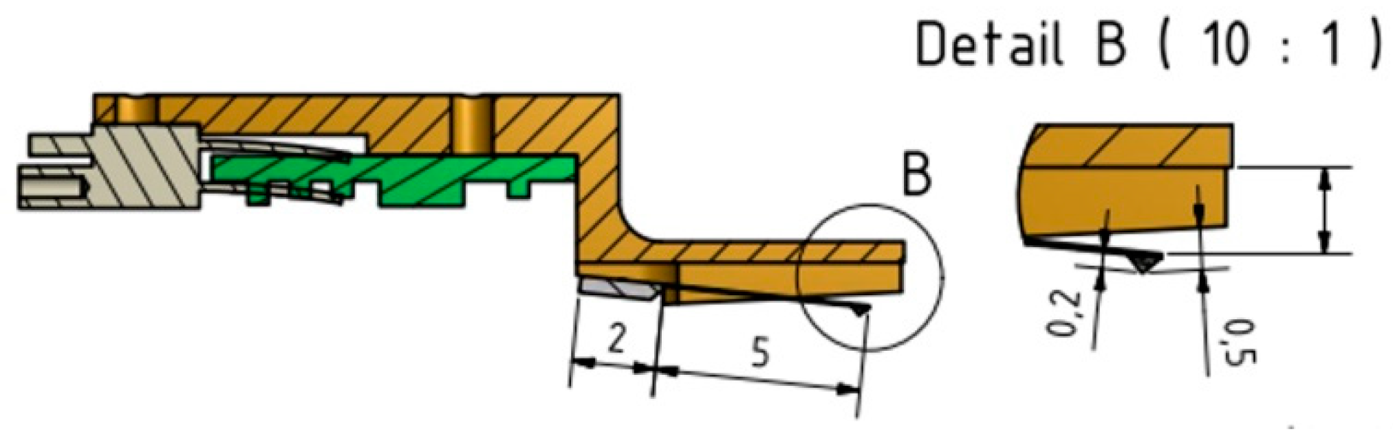
2.3. Tip Form Measurement
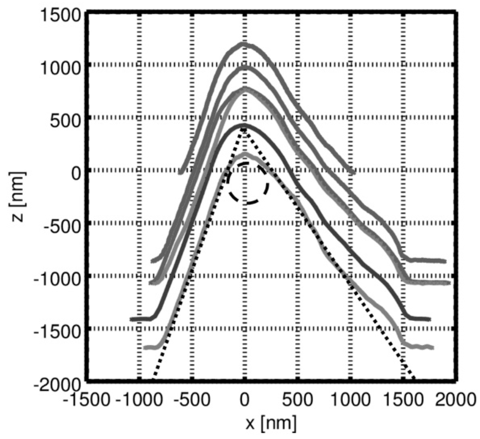
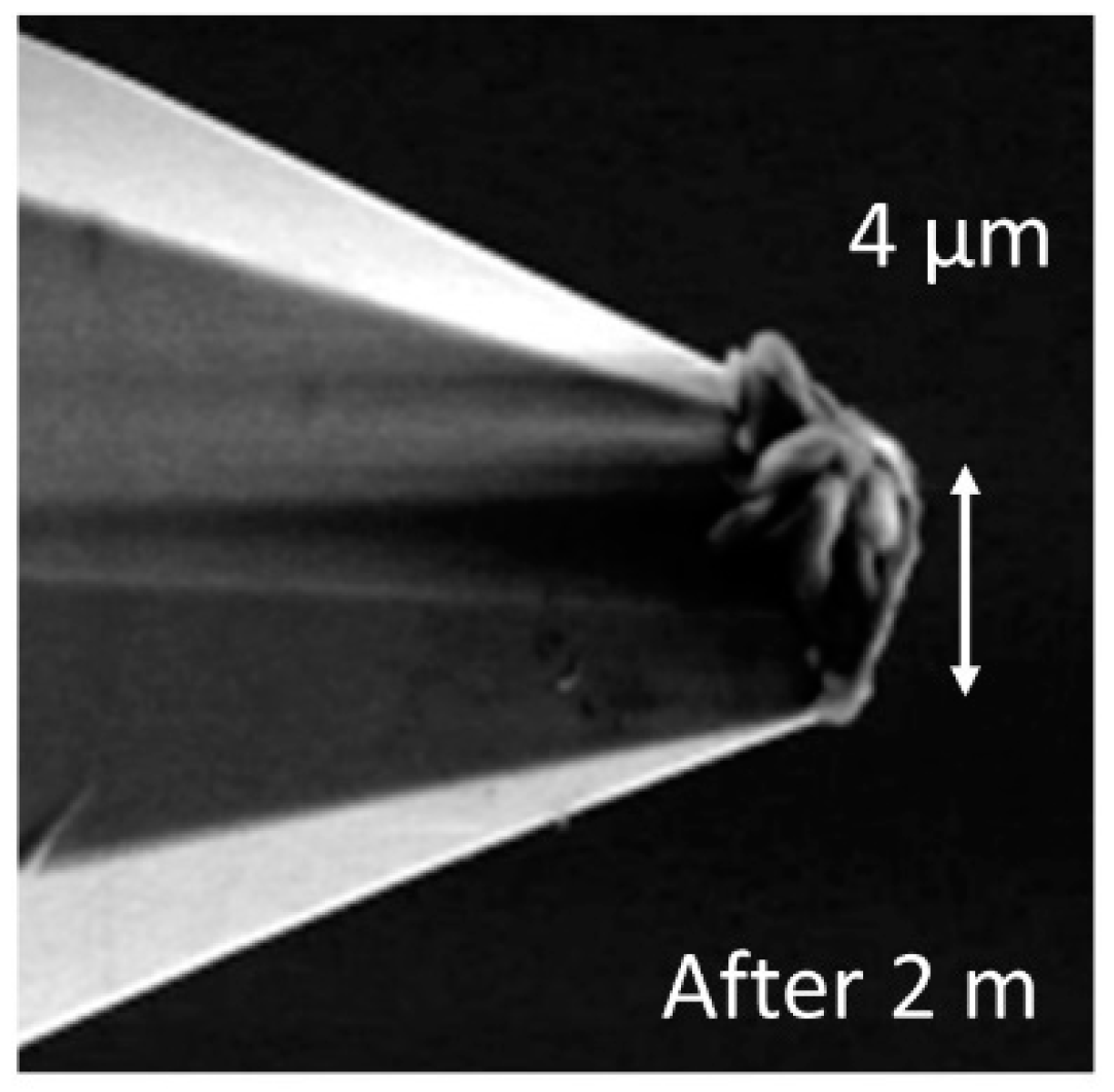
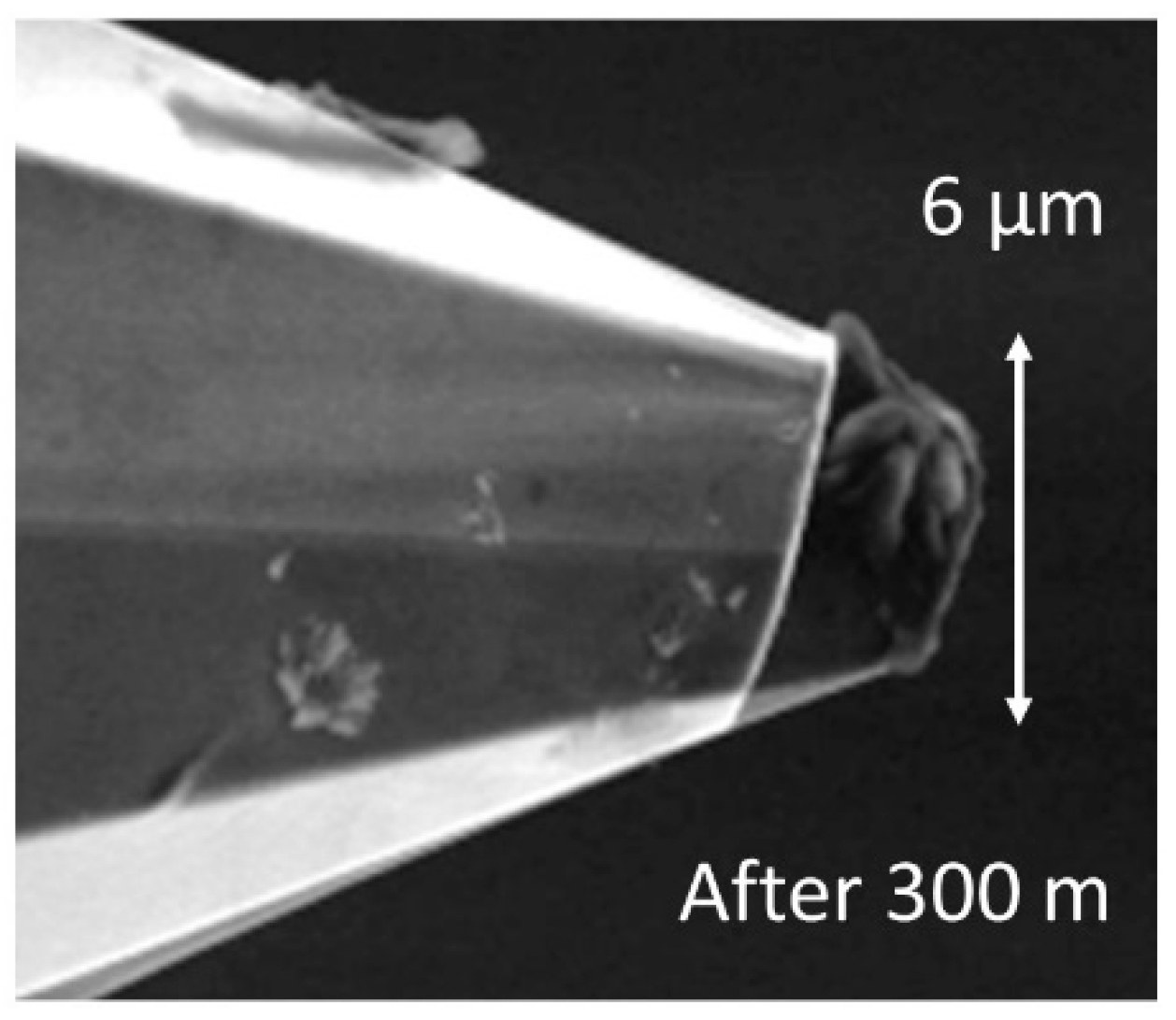
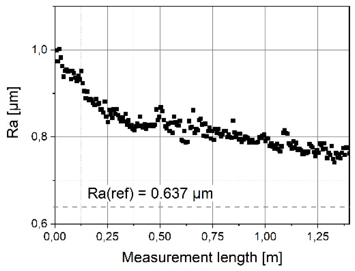
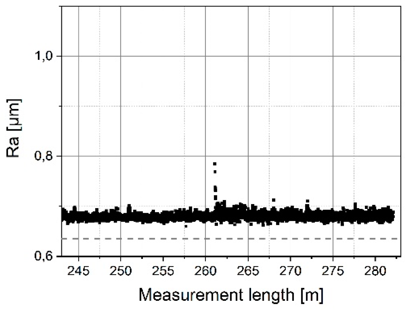
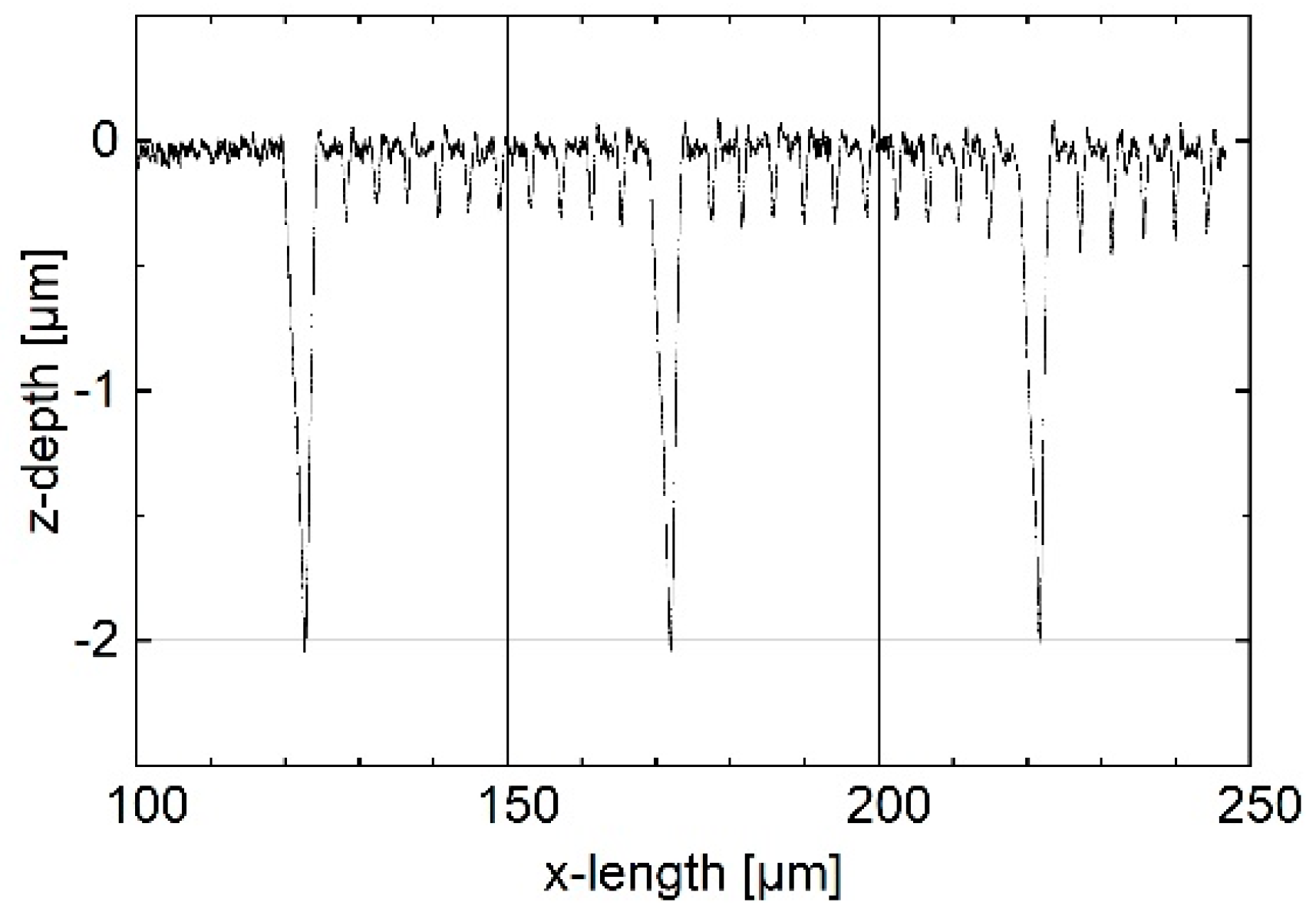
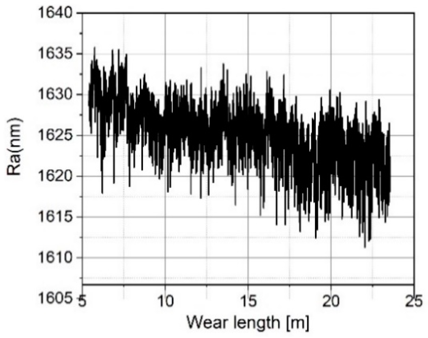
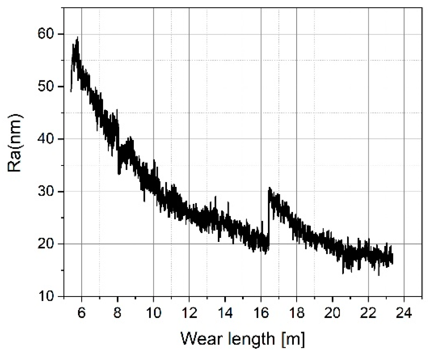
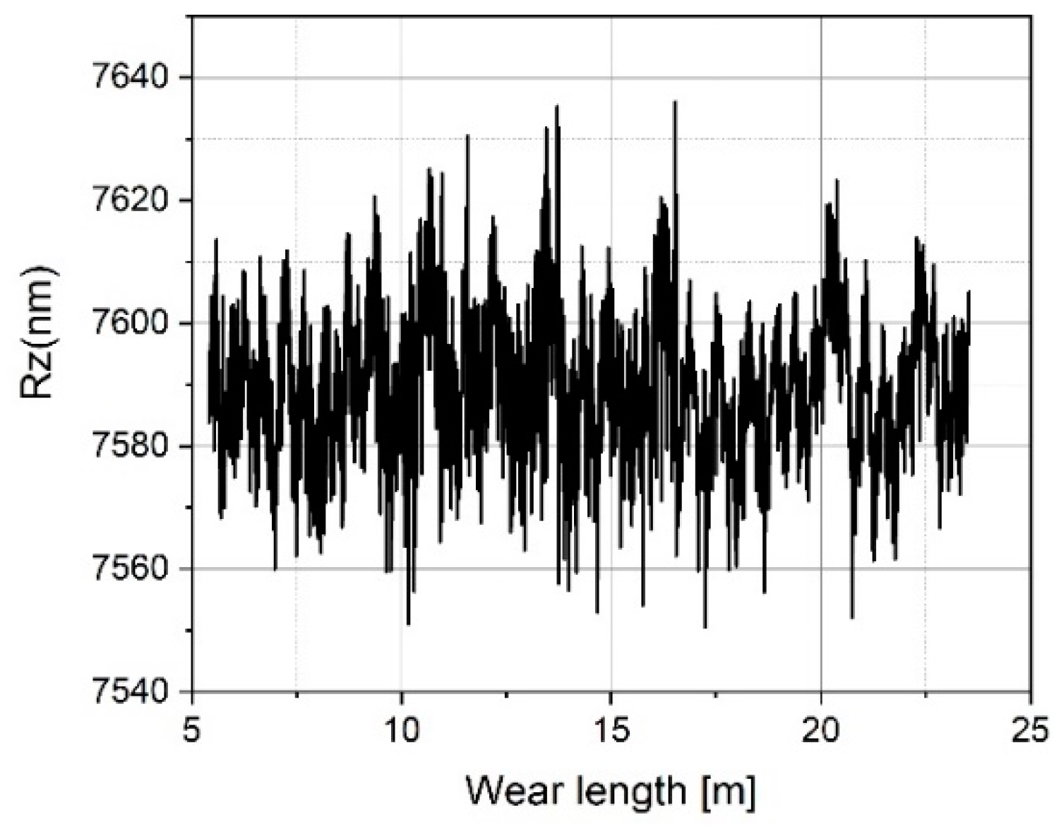
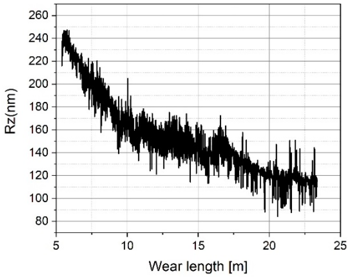
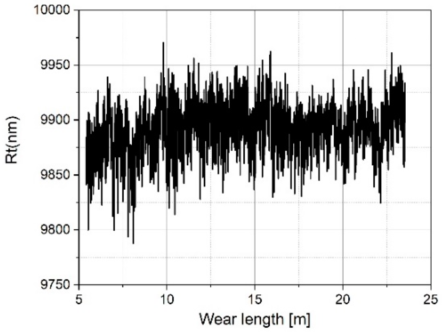
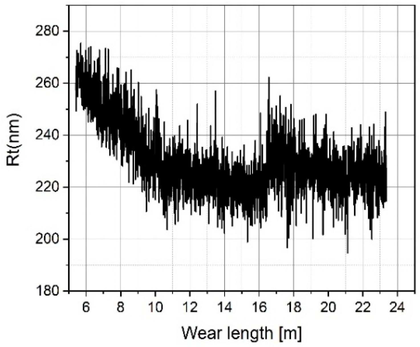
2.4. Tip Wear
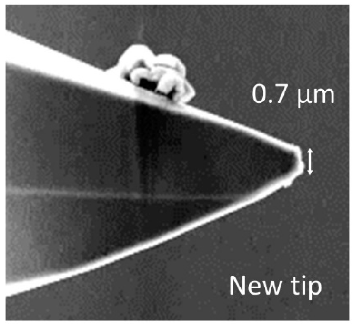
2.4.1. Silicon Tips
Wear Protective Layer
2.4.2. Diamond Tips
2.5. Probing Force
3. Currently Available Instruments Equipped with Piezo-Resistive Microprobes
3.1. A Traceable Profilescanner for Measurements inside High-Aspect Ratio Microstructures
3.2. A Miniaturized MicroProfiler with an Integrated Feed Unit
4. Experimental Results
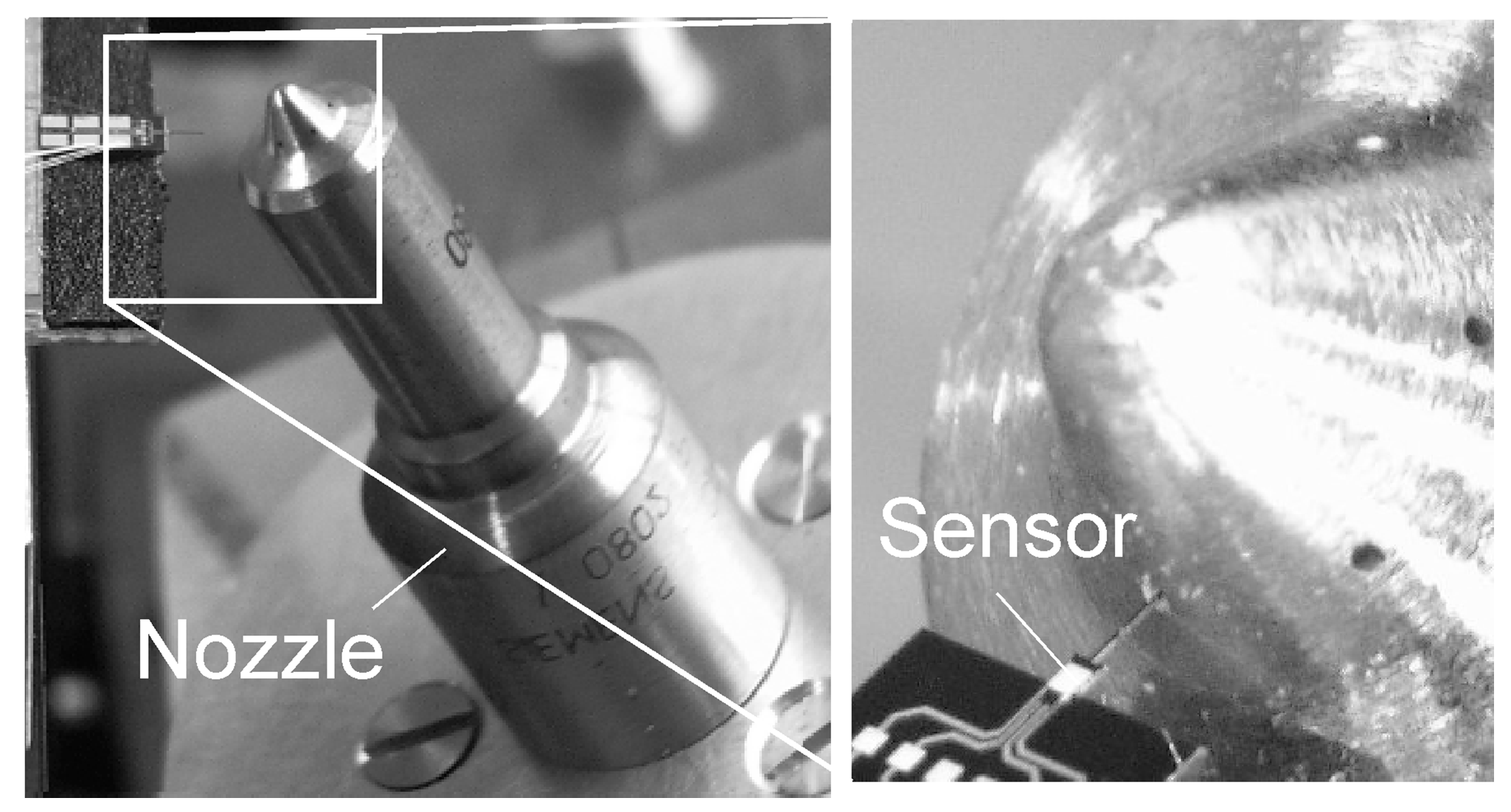
4.1. Measurement of Roughness and Form Deviation inside Micro-Nozzles
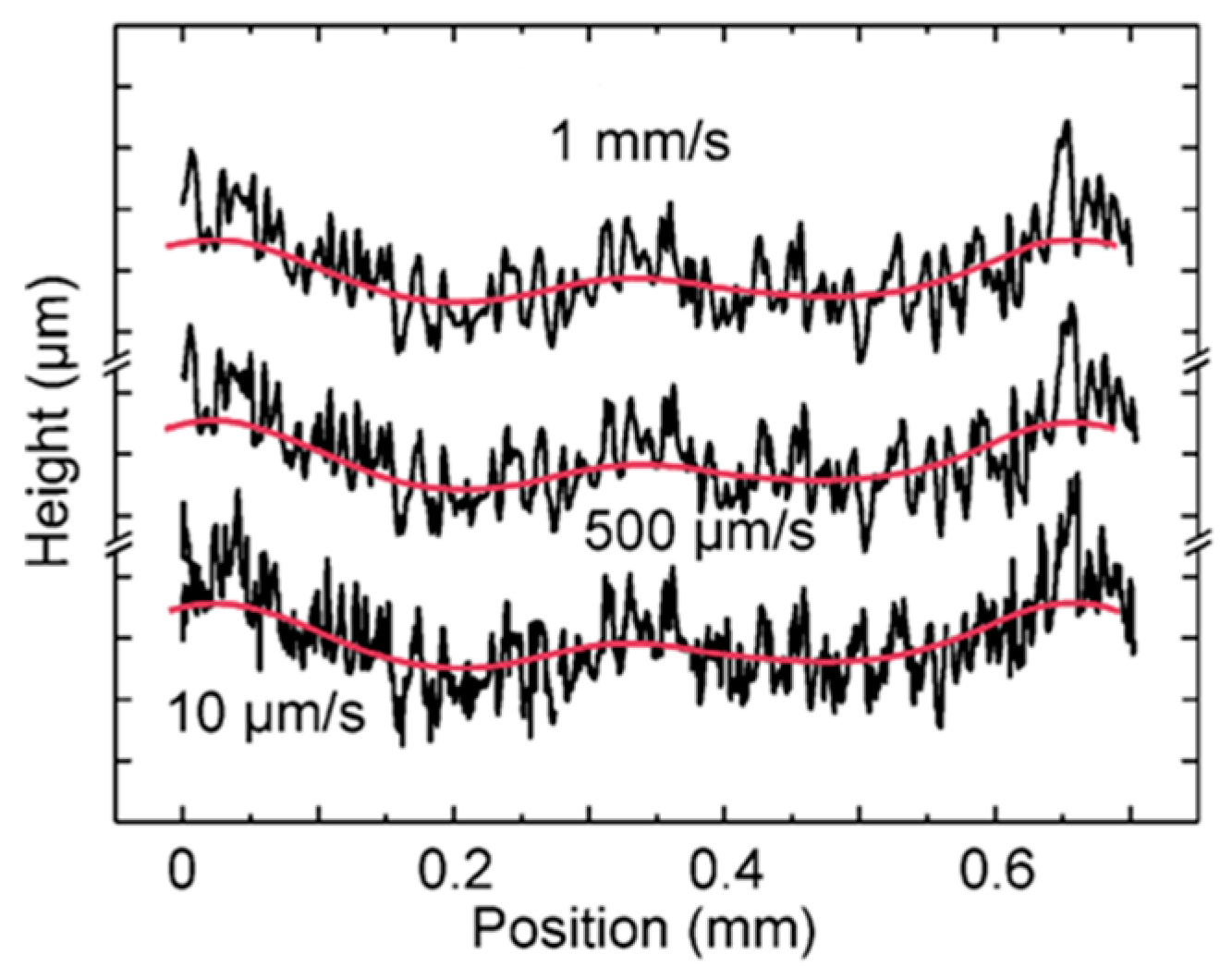
4.1.1. Critical Flow Venturi Nozzles (Sonic Nozzles) for Gas Flow Measurements
4.1.2. Diesel Injection Nozzles
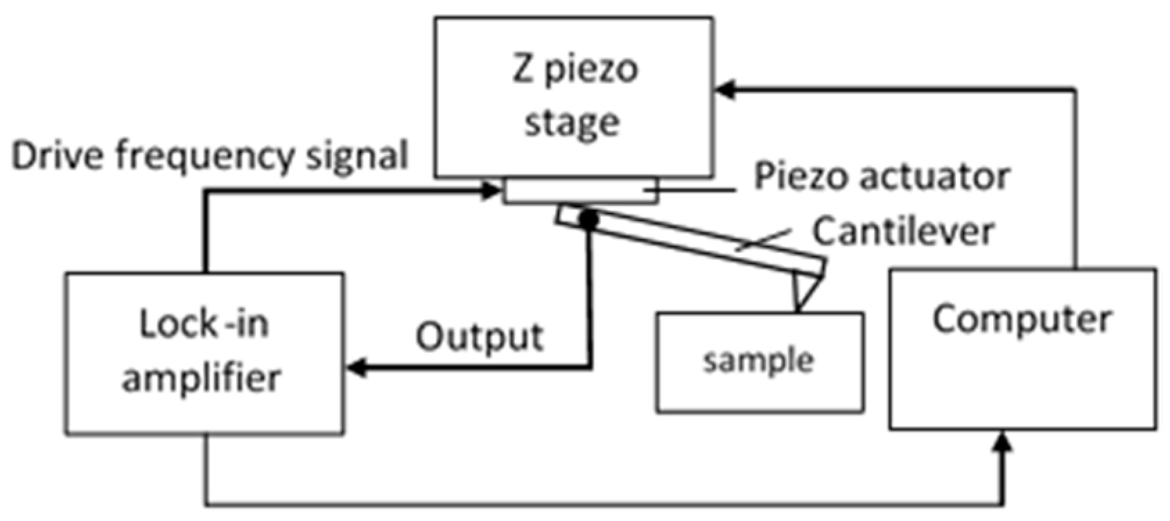
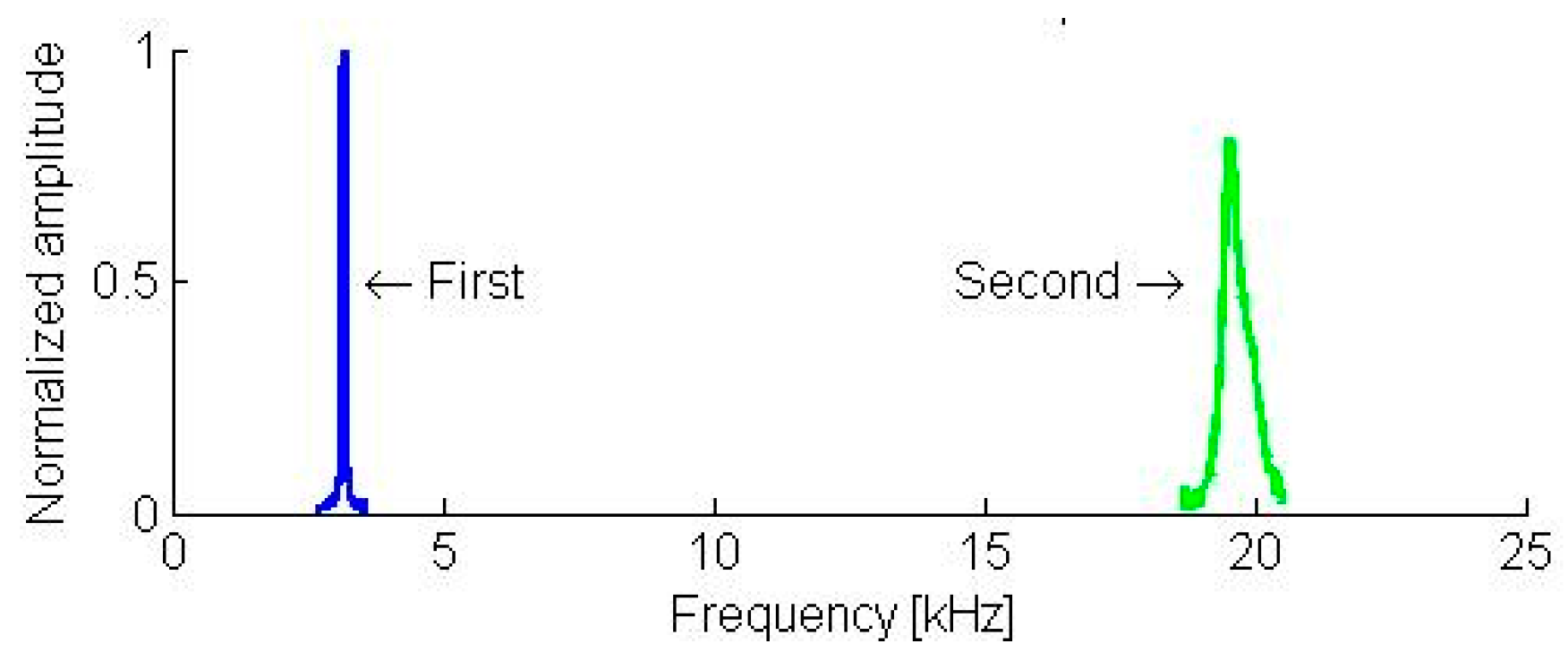
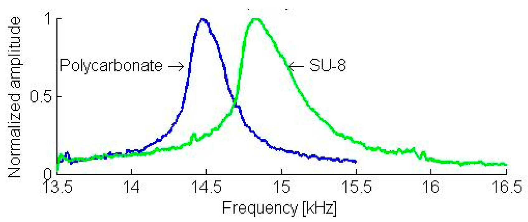
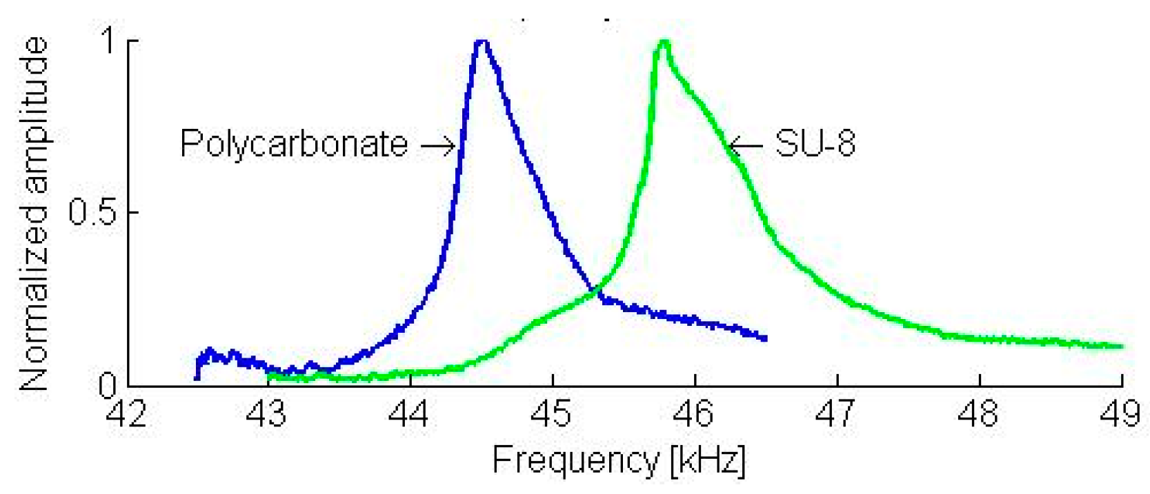
4.2. Mechanical Properties Measurement via Contact Resonance
5. Summary
Author Contributions
Funding
Acknowledgments
Conflicts of Interest
References
- Dai, G.; Wolff, H.; Danzebrink, H.-U. Atomic force microscope cantilever based microcoordinate measuring probe for true three-dimensional measurements of microstructures. Appl. Phys. Lett. 2007, 91, 121912. [Google Scholar] [CrossRef]
- Schwenke, H.; Wäldele, F.; Weiskirch, C.; Kunzmann, H. Opto-tactile Sensor for 2D and 3D Measurement of Small Structures on Coordinate Measuring Machines. CIRP Ann. 2001, 50, 361–364. [Google Scholar] [CrossRef]
- Peiner, E.; Doering, L. Nondestructive Evaluation of Diesel Spray Holes Using Piezoresistive Sensors. IEEE Sens. J. 2013, 13, 701–708. [Google Scholar] [CrossRef]
- DIN EN ISO 3274:1998-04 Geometrical Product Specifications (GPS)—Surface Texture: Profile Method—Nominal Characteristics of Contact (Stylus) Instruments (ISO 3274:1996), German Version EN ISO 3274:1997. 1996. Available online: https://www.beuth.de/de/norm/din-en-iso-3274/3361735. (accessed on 21 March 2019).
- Peiner, E.; Doering, L.; Stranz, A. Surface finish improvement of deep micro bores monitored using an active MEMS cantilever probe. In Proceedings of the 2010 IEEE International Conference on Industrial Technology (ICIT), Vina del Mar, Chile, 14–17 March 2010; pp. 297–302. [Google Scholar]
- Min, X.; Uwe, B.; Jürgen, K. Traceable profilometer with a piezoresistive cantilever for high-aspect-ratio microstructure metrology. In Proceedings of the 13th euspen International Conference, Berlin, Germany, 27–31 May 2013. [Google Scholar]
- Doering, L.; Brand, U.; Bütefisch, S.; Ahbe, T.; Weimann, T.; Peiner, E.; Frank, T. High-speed microprobe for roughness measurements in high-aspect-ratio microstructures. Meas. Sci. Technol. 2017, 28, 034009. [Google Scholar] [CrossRef]
- EU EMPIR Project MicroProbes. Available online: https://www.ptb.de/empir2018/microprobes/project/ (accessed on 6 December 2018).
- Brand, U.; Gao, S.; Doering, L.; Li, Z.; Xu, M.; Buetefisch, S.; Peiner, E.; Fruehauf, J.; Hiller, K. Smart sensors and calibration standards for high precision metrology. Vol. Proc. SPIE 2015, 9517, 95170V. [Google Scholar]
- Fritsch, H.; Lucklum, R.; Iwert, T.; Hauptmann, P.; Scholz, D.; Peiner, E.; Schlachetzki, A. A low-frequency micromechanical resonant vibration sensor for wear monitoring. Sens. Actuators Phys. 1997, 62, 616–620. [Google Scholar] [CrossRef]
- Peiner, E. Silizium-Sensorik für die Maschinenüberwachung; Shaker Verlag GmbH: Aachen, Germany, 2000; ISBN 978-3-8265-7401-6. (In Germany) [Google Scholar]
- Peiner, E.; Doering, L. Force Calibration of Stylus Instruments using silicon microcantilevers. Sens. Actuators Phys. 2005, 123–124, 137–145. [Google Scholar] [CrossRef]
- Peiner, E.; Balke, M.; Doering, L.; Brand, U. Tactile probes for dimensional metrology with microcomponents at nanometre resolution. Meas. Sci. Technol. 2008, 19, 064001. [Google Scholar] [CrossRef]
- Microprobes for In-Line Surface Inspection in Manufacturing Machines. CiS Forschungsinstitut für Mikrosensorik GmbH Konrad-Zuse-Straße 14, 99099 Erfurt (Germany). Available online: https://www.cismst.org/aktuelles/newsarchiv/newsdetail/news-2014-01-24/ (accessed on 8 January 2019).
- Peiner, E.; Balke, M.; Doering, L. Slender tactile sensor for contour and roughness measurements within deep and narrow holes. Sens. J. IEEE 2008, 8, 1960–1967. [Google Scholar] [CrossRef]
- Xu, M.; Kauth, F.; Mickan, B.; Brand, U. Traceable profile and roughness measurements inside small sonic nozzles with the Profilscanner to analyse the influence of inner topography on the flow rate characters. Meas. Sci. Technol. 2016, 27, 094001. [Google Scholar] [CrossRef]
- ACNano Ultraclam Acoustic Isolator Hood and Mechanical Noise Isolation Chamber from Novascan Technologies, Inc. Novascan Research Building, 131 Main Street, Ames, IA 50010-6359, USA. Available online: https://www.novascan.com/products/acoustic_isolation.php (accessed on 21 March 2019).
- Data aquisition system MGC plus with ML10B amplifier module from Hottinger Baldwin Messtechnik GmbH. Im Tiefen See 45, 64293 Darmstadt (Germany). Available online: https://www.hbm.com/en/2261/mgcplus-modular-data-acquisition-system/ (accessed on 21 March 2019).
- PTB’s Online Reference Software for Roughness Measurements. Available online: https://www.ptb.de/rptb (accessed on 7 December 2018).
- ISO 16610-40:2015(en), Geometrical Product Specifications (GPS)—Filtration—Part 40: Morphological Profile Filters: Basic Concepts. Available online: https://www.iso.org/obp/ui/#iso:std:iso:16610:-40:ed-1:v2:en (accessed on 12 December 2018).
- ISO 16610-41:2015 Geometrical Product Specifications (GPS)—Filtration—Part 41: Morphological Profile Filters: Disk and Horizontal Line-Segment Filters. Available online: https://www.iso.org/standard/61380.html (accessed on 21 March 2019).
- ISO 13095:2014—Surface Chemical Analysis—Atomic Force Microscope—Procedure for In Situ Characterization of AFM Probe Shank Profile Used for Nanostructure Measurement. 2015. Available online: https://www.iso.org/standard/52800.html (accessed on 21 March 2019).
- Itoh, H.; Fujimoto, T.; Ichimura, S. Tip characterizer for atomic force microscopy. Rev. Sci. Instrum. 2006, 77, 103704. [Google Scholar] [CrossRef]
- German standard DIN 32567-3:2014-10 Production equipment for microsystems—Determination of the influence of materials on the optical and tactile dimensional metrology—Derivation of correction values for tactile measuring devices. Available online: https://www.beuth.de/en/standard/din-32567-3/215490275 (accessed on 21 March 2019).
- Whitehouse, D.J. Handbook of Surface Metrology. Available online: https://www.crcpress.com/Handbook-of-Surface-Metrology/Whitehouse/p/book/9780750300391 (accessed on 20 December 2018).
- UHU Plus Endfest Solvent Free 2-Component Epoxy Resin Adhesive from UHU GmbH & Co. KG, Herrmannstraße 7, D - 77815 Bühl/Baden (Germany). Available online: https://www.uhu-profishop.de/klebstoffe/2-komponenten-klebstoffe/uhu-plus-klebstoffe/?gclid=CjwKCAjw7MzkBRAGEiwAkOXexKTOjI5z3bNeVlxiB1qepP5PvzLoiJhGnPmKYJAWXVWSXHo3_x5SgBoCrsoQAvD_BwE (accessed on 21 March 2019).
- Cantilever type silicon force standard FS-C from the SiMetrics GmbH, Am Südhang 5, 09212 Limbach-Oberfrohna (Germany). Available online: https://www.simetrics.de/pdf/FS-C.pdf (accessed on 21 March 2019).
- Bridge type silicon force standard FS-B from the SiMetrics GmbH, Am Südhang 5, 09212 Limbach-Oberfrohna (Germany). Available online: https://www.simetrics.de/pdf/FS-B.pdf (accessed on 21 March 2019).
- Kim, M.-S.; Pratt, J.R.; Brand, U.; Jones, C.W. Report on the first international comparison of small force facilities: A pilot study at the micronewton level. Metrologia 2012, 49, 70–81. [Google Scholar] [CrossRef]
- FT-S Microforce Sensing Probe from FemtoTools AG, Furtbachstrasse 4, 8107 Buchs/ZH (Switzerland). Available online: https://www.femtotools.com/products/previousproducts/ft-s-microforce-sensing-probe/ (accessed on 21 March 2019).
- Meander type force sensor with large loading area for forces up to 1 mN from the CiS Forschungsinstitut für Mikrosensorik GmbH, Konrad-Zuse-Straße 14, 99099 Erfurt (Germany). Available online: https://www.cismst.org/en/technologien/technologien-start/ (accessed on 21 March 2019).
- Hamdana, G.; Bertke, M.; Doering, L.; Frank, T.; Brand, U.; Wasisto, H.S.; Peiner, E. Transferable micromachined piezoresistive force sensor with integrated double-meander-spring system. J. Sens. Sens. Syst. 2017, 6, 121–133. [Google Scholar] [CrossRef]
- Aeschbacher, M.; Wüthrich, C.; Marti, K.; Brand, U. Comparison measurement of commercially available capacitive force sensors between METAS and PTB. 2019; to be published. [Google Scholar]
- Xu, M.; Kirchhoff, J.; Brand, U. Development of a traceable profilometer for high-aspect-ratio microstructures metrology. Surf. Topogr. Metrol. Prop. 2014, 2, 024002. [Google Scholar] [CrossRef]
- MicroProfiler with silicon microprobes and integrated traverse unit from Breitmeier Messtechnik GmbH, Im Stöck 4 a, 76275 Ettlingen (Germany). Available online: https://www.breitmeier.de/Download/pdf/MicroProfiler-B_170621_D.pdf (accessed on 21 March 2019).
- Sinusoidal roughness artefact PGN 3 with 3 µm depth from Mahr GmbH, Carl-Mahr-Str. 1, 37073 Göttingen (Germany). Available online: https://www.mahr.com/de/Leistungen/Fertigungsmesstechnik/Der-News--und-Praxis-Blog/?BlogContentID=20963&Blog_action=comment (accessed on 21 March 2019).
- Xu, M.; Kauth, F.; Mickan, B.; Brand, U. Traceable Profile and Roughness Measurements Inside Micro Sonic Nozzles with the Profilscanner. In Proceedings of the 17th International Congress of Metrology, Paris, France, 21–24 September 2015; p. 13004. [Google Scholar]
- Mickan, B.; Kuo, M.; Xu, M. Systematic investigation of cylindrical nozzles acc. ISO 9300 down to throat diamters of 125 µm. In Proceedings of the 10th ISFFM 2018, Queretaro, Mexico, 21–23 March 2018. [Google Scholar]
- Peiner, E.; Balke, M.; Doering, L. Form measurement inside fuel injector nozzle spray holes. Microelectron. Eng. 2009, 86, 984–986. [Google Scholar] [CrossRef]
- Sahin, O.; Erina, N. High-resolution and large dynamic range nanomechanical mapping in tapping-mode atomic force microscopy. Nanotechnology 2008, 19, 445717. [Google Scholar] [CrossRef] [PubMed]
- Young, T.J.; Monclus, M.A.; Burnett, T.L.; Broughton, W.R.; Ogin, S.L.; Smith, P.A. The use of the PeakForce TM quantitative nanomechanical mapping AFM-based method for high-resolution Young’s modulus measurement of polymers. Meas. Sci. Technol. 2011, 22, 125703. [Google Scholar] [CrossRef]
- Xu, M.; Brand, U.; Koenders, L. Characterizing the material mechanical properties inside small holes. In Proceedings of the Euspen 17th Int. Conf. & Exhib., Hannover, Germany, 29 May–2 June 2017. [Google Scholar]
- Arnold, W.; Caron, A.; Hirsekorn, S.; Kopycinska-Müller, M.; Rabe, U.; Reinstädtler, M. Atomic Force Microscopy at Ultrasonic Frequencies. In Fracture Mechanics of Ceramics; Bradt, R.C., Munz, D., Sakai, M., White, K.W., Eds.; Springer: Boston, MA, USA, 2005; pp. 1–11. [Google Scholar]
- Hamdana, G.; Puranto, P.; Langfahl-Klabes, J.; Li, Z.; Pohlenz, F.; Xu, M.; Granz, T.; Bertke, M.; Wasisto, H.S.; Brand, U.; et al. Nanoindentation of crystalline silicon pillars fabricated by soft UV nanoimprint lithography and cryogenic deep reactive ion etching. Sens. Actuators Phys. 2018, 283, 65–78. [Google Scholar] [CrossRef]
- Li, Z.; Brand, U.; Ahbe, T. Towards quantitative modelling of surface deformation of polymer micro-structures under tactile scanning measurement. Meas. Sci. Technol. 2014, 25, 044010. [Google Scholar] [CrossRef]


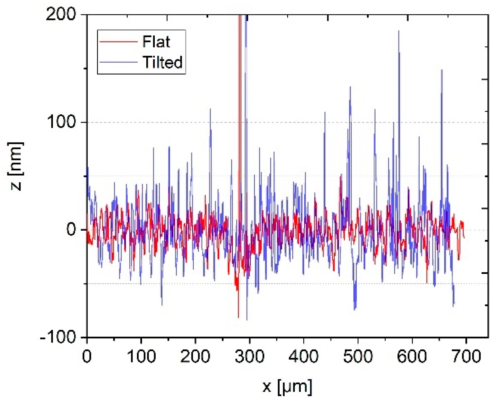
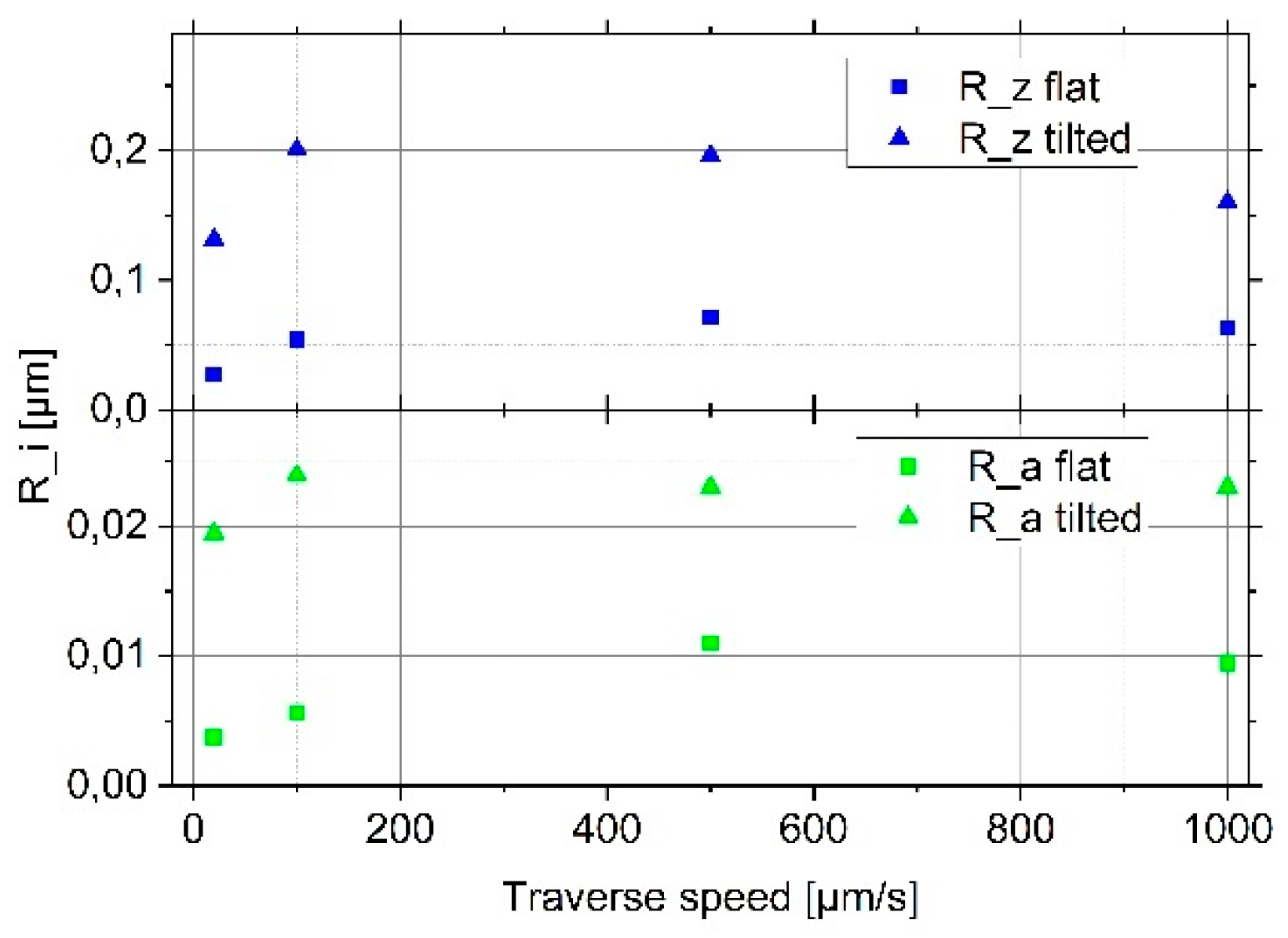
| Traverse | No Tilt/100 µm Tilt | |
|---|---|---|
| Speed (µm/s) | Rz (nm) | Ra (nm) |
| 20 | 27(6)/131(30) | 3.7(0.6)/19(4) |
| 100 | 54(11)/201(63) | 5.6(0.9)/24(8) |
| 500 | 71(21)/196(68) | 11(2)/23(3) |
| 1000 | 63(21)/160(30) | 9.4(1.6)/23(2) |
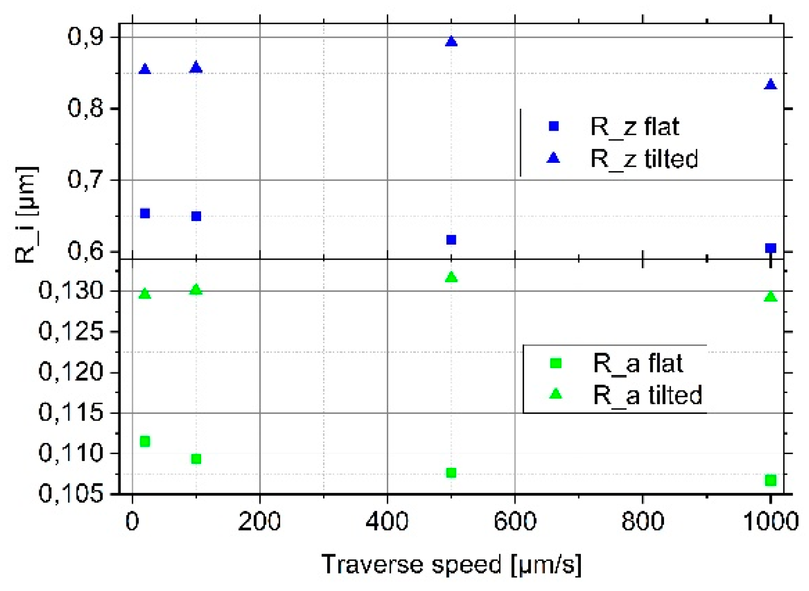
| Traverse | No Tilt/100 µm Tilt | |
|---|---|---|
| Speed (µm/s) | Rz (nm) | Ra (nm) |
| 20 | 654(156)/854(113) | 111(26)/130(13) |
| 100 | 649(153)/857(103) | 109(27)/130(14) |
| 500 | 617(160)/893(129) | 108(28)/132(16) |
| 1000 | 605(152)/833(156) | 107(23)/129(22) |
| Measurement range (x × y × z) | 800 µm × 800 µm × 250 µm |
| Stage travelling distance (x × y × z) | 50 mm × 50 mm × 12 mm |
| Rotary stage continuous | 360° |
| Maximum artefact size (x × y × z) | 80 mm × 100 mm × 100 mm |
| Minimum probing force | 1 µN |
| Maximum scanning rate | 1 mm s−1 |
| Maximum sampling rate | 19.2 kHz |
| Data points per scan line | 65 536 maximum |
| Available microprobe length | 1.25, 3 and 5 mm |
| Tip radius Si/diamond | < 0.1 µm/2 µm |
| Parameter | Value |
|---|---|
| Cantilever length, width, height | 1.25 mm/30 µm/25 µm |
| Operation temperature | −20 °C … +80 °C |
| Sensitivity | (4.0 ± 0.3) nm/µV/V |
| Temperature coefficient | (0.31 ± 0.1) %/K |
| (−2 ± 10) µV/V/K | |
| Noise (1.6 kHz bandwidth, amplifier 0.4 µV/V) | 2.4 nm |
| Light susceptibility (cold light 0.1 mW/cm2) | 9.2 nm |
| Tip height/radius | (15 – 25) µm/< 100 nm |
| Cone angle | (40 ± 2) ° |
| Tip wear (100 µN static force) | 0.1 nm/m |
| Fracture limit axial/lateral/vertical | 170/520/470 µm deflection |
| Resonance frequency | 46.4 kHz |
© 2019 by the authors. Licensee MDPI, Basel, Switzerland. This article is an open access article distributed under the terms and conditions of the Creative Commons Attribution (CC BY) license (http://creativecommons.org/licenses/by/4.0/).
Share and Cite
Brand, U.; Xu, M.; Doering, L.; Langfahl-Klabes, J.; Behle, H.; Bütefisch, S.; Ahbe, T.; Peiner, E.; Völlmeke, S.; Frank, T.; et al. Long Slender Piezo-Resistive Silicon Microprobes for Fast Measurements of Roughness and Mechanical Properties inside Micro-Holes with Diameters below 100 µm. Sensors 2019, 19, 1410. https://doi.org/10.3390/s19061410
Brand U, Xu M, Doering L, Langfahl-Klabes J, Behle H, Bütefisch S, Ahbe T, Peiner E, Völlmeke S, Frank T, et al. Long Slender Piezo-Resistive Silicon Microprobes for Fast Measurements of Roughness and Mechanical Properties inside Micro-Holes with Diameters below 100 µm. Sensors. 2019; 19(6):1410. https://doi.org/10.3390/s19061410
Chicago/Turabian StyleBrand, Uwe, Min Xu, Lutz Doering, Jannick Langfahl-Klabes, Heinrich Behle, Sebastian Bütefisch, Thomas Ahbe, Erwin Peiner, Stefan Völlmeke, Thomas Frank, and et al. 2019. "Long Slender Piezo-Resistive Silicon Microprobes for Fast Measurements of Roughness and Mechanical Properties inside Micro-Holes with Diameters below 100 µm" Sensors 19, no. 6: 1410. https://doi.org/10.3390/s19061410
APA StyleBrand, U., Xu, M., Doering, L., Langfahl-Klabes, J., Behle, H., Bütefisch, S., Ahbe, T., Peiner, E., Völlmeke, S., Frank, T., Mickan, B., Kiselev, I., Hauptmannl, M., & Drexel, M. (2019). Long Slender Piezo-Resistive Silicon Microprobes for Fast Measurements of Roughness and Mechanical Properties inside Micro-Holes with Diameters below 100 µm. Sensors, 19(6), 1410. https://doi.org/10.3390/s19061410