Abstract
A submicron pixel’s light and dark performance were studied by experiment and simulation. An advanced node technology incorporated with a stacked CMOS image sensor (CIS) is promising in that it may enhance performance. In this work, we demonstrated a low dark current of 3.2 e−/s at 60 °C, an ultra-low read noise of 0.90 e−·rms, a high full well capacity (FWC) of 4100 e−, and blooming of 0.5% in 0.9 μm pixels with a pixel supply voltage of 2.8 V. In addition, the simulation study result of 0.8 μm pixels is discussed.
1. Introduction
Scaling down pixel size is absolutely necessary for high resolution imaging and quanta image sensors []. Recently, dual camera applications have become a major trend in the smartphone market [], in which a small pixel size image sensor can be used as be a high resolution image sensor for the purpose of producing a zoomed image. In addition, phase detection auto focus function has developed. Among various pixel types of the function, dual photodiode phase detection auto focus also needs equivalently small pixel size [].
However, sensor performances of the small pixel are generally inferior to those of previous generations with larger pixel sizes []. Major challenges in submicron pixel generation are shown in Figure 1. A small pixel does not have enough space for a large source follower device and a large photodiode. This induces higher source follower noise and a smaller fill factor. These in turn influence the dynamic range and the signal-to-noise ratio (SNR). Additionally, the required implant dosage is higher for smaller pixels, and a higher implant dosage will induce higher dark currents and white pixels due to ion implant damage. Moreover, crosstalk is significant due to a small pixel pitch. These two problems significantly affect image quality.
Figure 1.
Challenges in submicron pixel generation. (a) Top view of pixel layout highlights the small size source follower; (b) top view of pixel layout indicating the small fill factor; (c) cross-sectional view of pixel depicting high ion implant damage induced by the high dose photodiode; (d) cross-sectional view of pixel showing high optical crosstalk.
Backside illumination technology has been developed and has enabled drastic S/N improvement [,]. Stacked CMOS image sensor (CIS) chips enable a more flexible manufacturing process dedicated to image sensors []. Furthermore, an advanced node technology [] with a stacked CIS might boost the light signal, reduce noise, and control the process variation caused by critical dimension fluctuations and mask overlay errors, which are more serious in submicron pixel generation.
In this paper, a silicon result of 0.9 μm pixels with well-balanced light and dark performance, making full use of a highly manufacturable 45 nm advanced technology with a stacked CMOS image sensor [], and 0.8 μm pixel simulation data are presented.
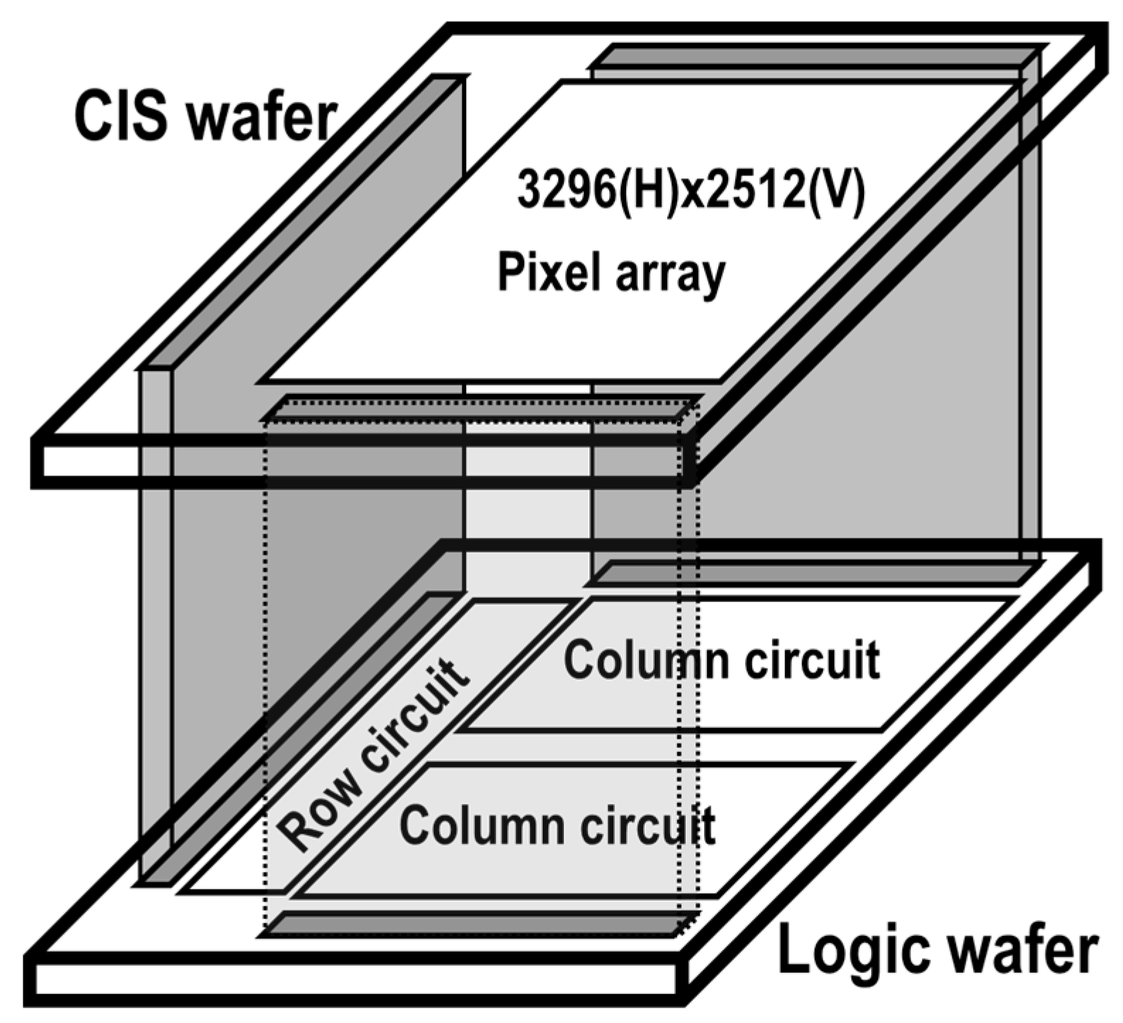
2. A 45 nm Stacked CMOS Image Sensor
The test chip architecture is an 8-mega-pixel (3296(H) × 2512(V)) raw data output CIS test vehicle. The block diagram of the vehicle is illustrated in Figure 2. The image sensor consists of two silicon layers. The top wafer comprises a pixel array and the bottom wafer comprises a read out circuit. Since a stacked CIS chip has a small camera module and a flexible design, a column level bonding stacked CIS architecture was adopted.
Figure 2.
Block diagram of 45 nm stacked CIS test vehicle.
There are two possibilities in terms of pixel device placement in a stacked CIS chip. One is to place it on a CIS wafer, and the other is to place it on a logic wafer. Table 1 summarizes the pros and cons of these two choices. Pixel devices on a CIS wafer lead to a highly flexible pixel device process but a lower full well capacity (FWC) due to a lower fill factor. On the other hand, pixel devices on a logic wafer lead to a higher FWC and have a simple pixel structure, consisting only of a transfer gate and a photodiode, but they have a lower conversion gain, which leads to higher noise, since the wiring between the logic wafer and the CIS wafer has some parasitic capacitance, and it is not negligible.
Table 1.
Pros and cons of two different methods of pixel device placement.
Taking into account the overall pixel performance, all pixel devices were placed on a CIS wafer, as shown in Figure 3. Since pixel devices were kept on a CIS wafer, advanced 45 nm technology was desired in terms of its low noise and high fill factor. The pixel architecture adopted a 2 × 2 shared 4-transistor without row-select, and the pixel unit cell size was 0.90 μm.
Figure 3.
A unit pixel circuit and device partition.
The processed CIS wafer was bonded with a logic wafer, followed by backside illumination process including thin down, anti-reflection coating, a color filter, and a micro-lens array process [].
3. Experimental Result
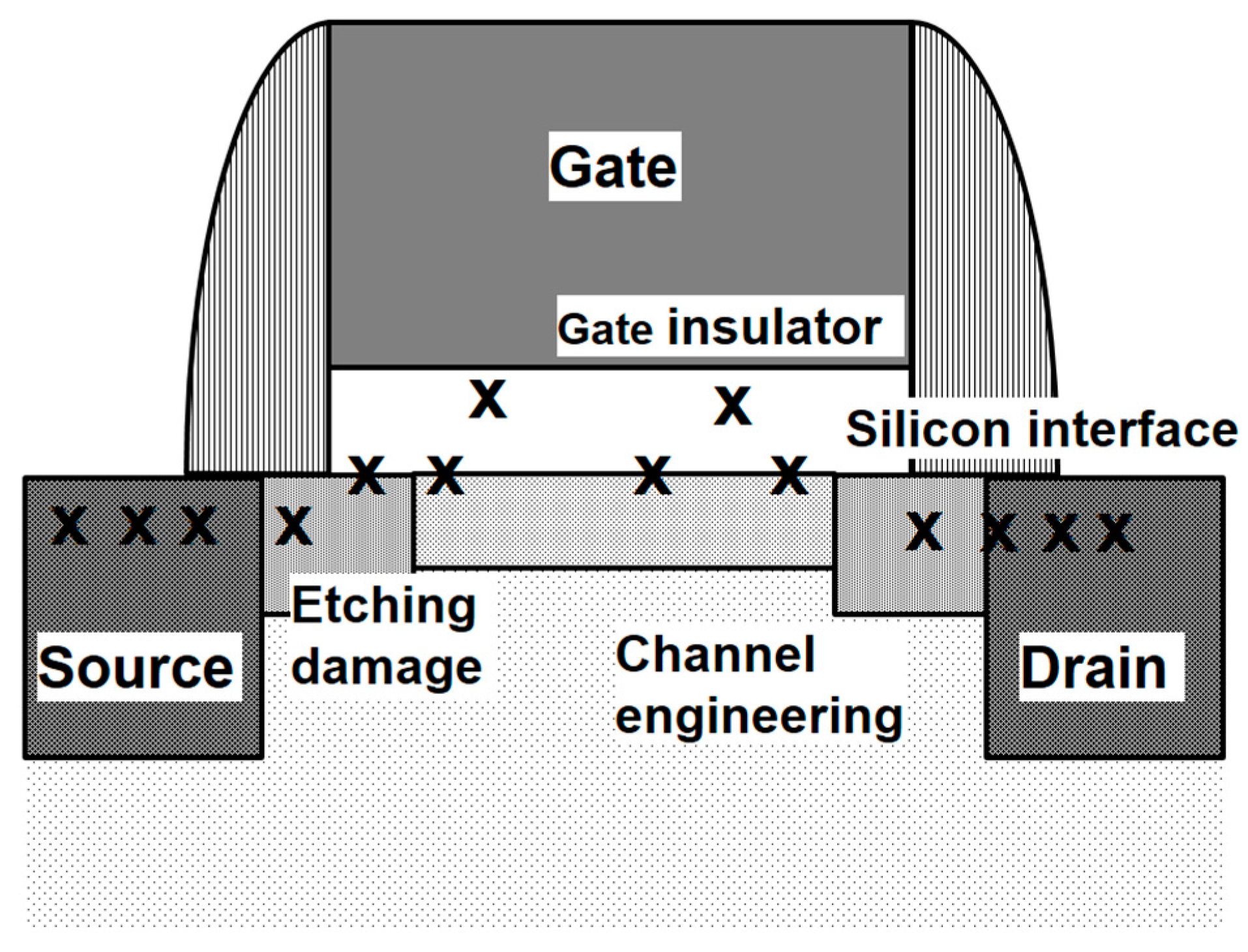
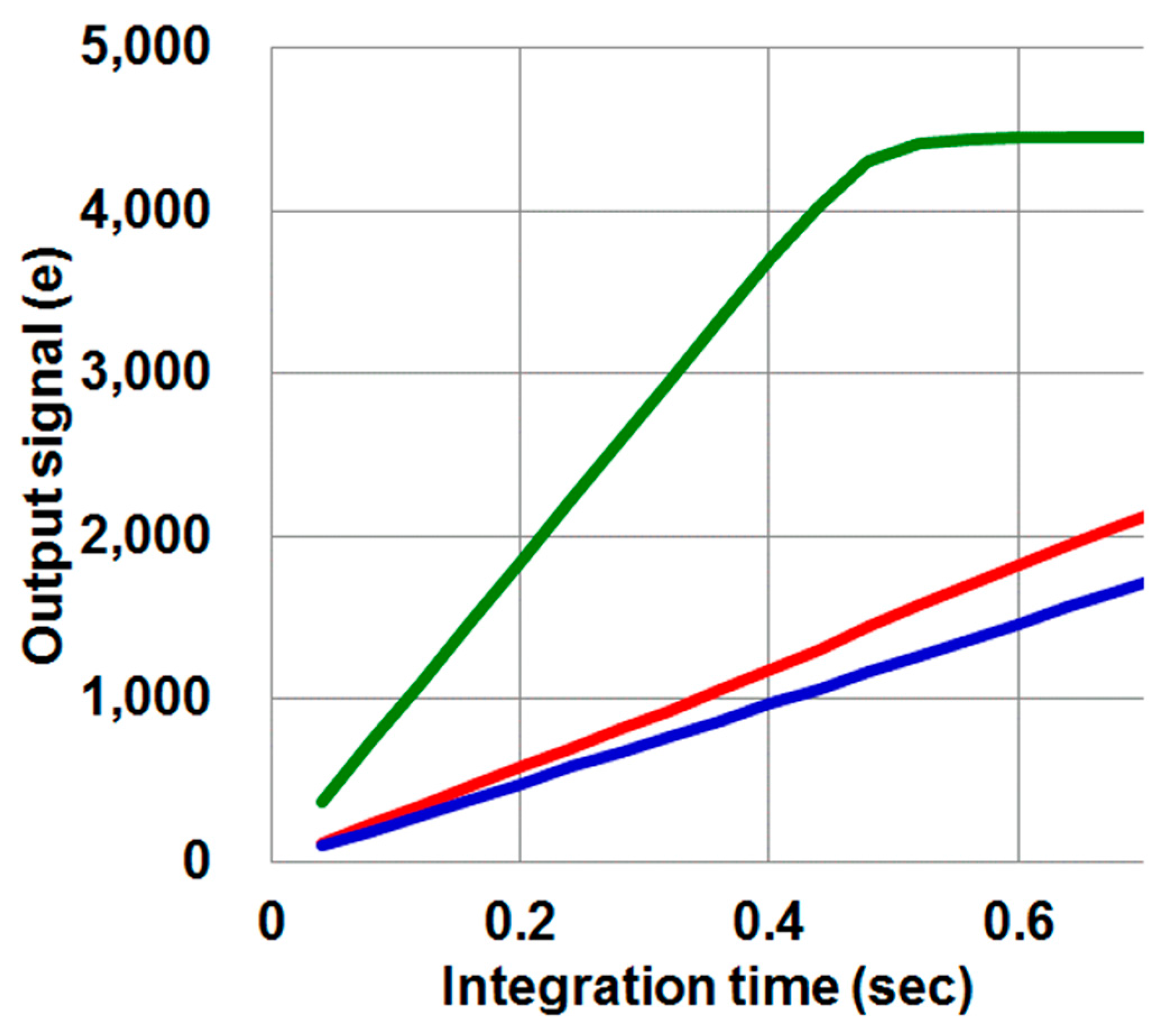
3.1. Low Noise Source Follower Device
An input referred noise in a conventional CIS is represented as follows []:
where N pixel, V circuit, and V source follower represent the noise generated at the pixel and the noise voltage generated in the circuit and source follower, respectively, Av is the circuit gain, CG is the conversion gain, Cox is the source follower gate capacitance, W is the source follower device width, L is the source follower device length, and N trap density is the trap state density.
It is clear from Equation (1) that increasing conversion gain is essential for reducing noise. A 45 nm design is beneficial for high conversion gain because the design rules are tighter than those of previous 65 nm node technology. The silicon result showed a conversion gain of 0.90 μm pixels reaching as high as 120 μV/e−.
After making an effort to reduce circuit noise, the signal chain noise was almost equivalent to the source follower flicker noise in the pixel array block, which was proportional to trap density and inversely proportional to gate capacitance, transistor width, and length.
Lithography capability is a key process element in this submicron pixel development. A 193 nm ArF immersion lithography was used for critical layers; as a result, the fill factor of 0.90 μm pixel increased by 20% with respect to the 65 nm technology. With the tightened design rules, the source follower device gate area can be maximized in a given small area in order to decrease random noise and random telegraph noise (RTN) []. The scaling of gate oxide thickness is also effective for random noise reduction [].
Traps influencing the source follower noise exist in the gate insulator, at the silicon interface, and in bulk, as shown in Figure 4. Thanks to the dedicated CIS wafer process, related processes, for instance, minimizing etching damage, eliminating dangling bonds, and device channel engineering, have been fully optimized [].
Figure 4.
Defects that influence the source follower device noise.
As a result, one of the key performance indexes, read noise, was reduced to 0.90 e−·rms at an analog gain of 18 dB, as shown in Figure 5, where the gray color indicates a 1.1 μm pixel with W = 0.2 μm and L = 0.8 μm, and the black color indicates a 0.9 μm pixel with W = 0.2 μm and L = 0.6 μm. Random telegraph noise, which contributes to the tail part of the distribution, also improved in spite of the smaller source follower device.
Figure 5.
Statistical read noise distributions of the 0.9 μm pixel and the 1.1 μm pixel at an analog gain of 18 dB.
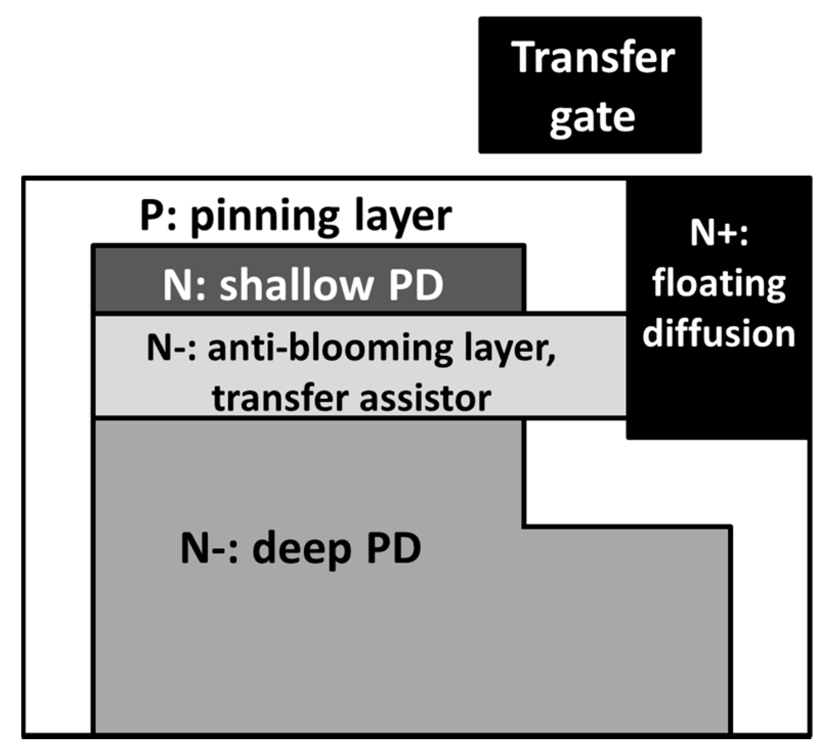
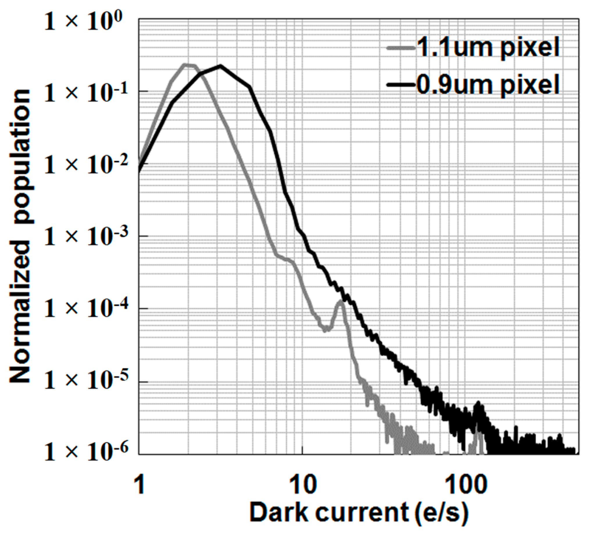
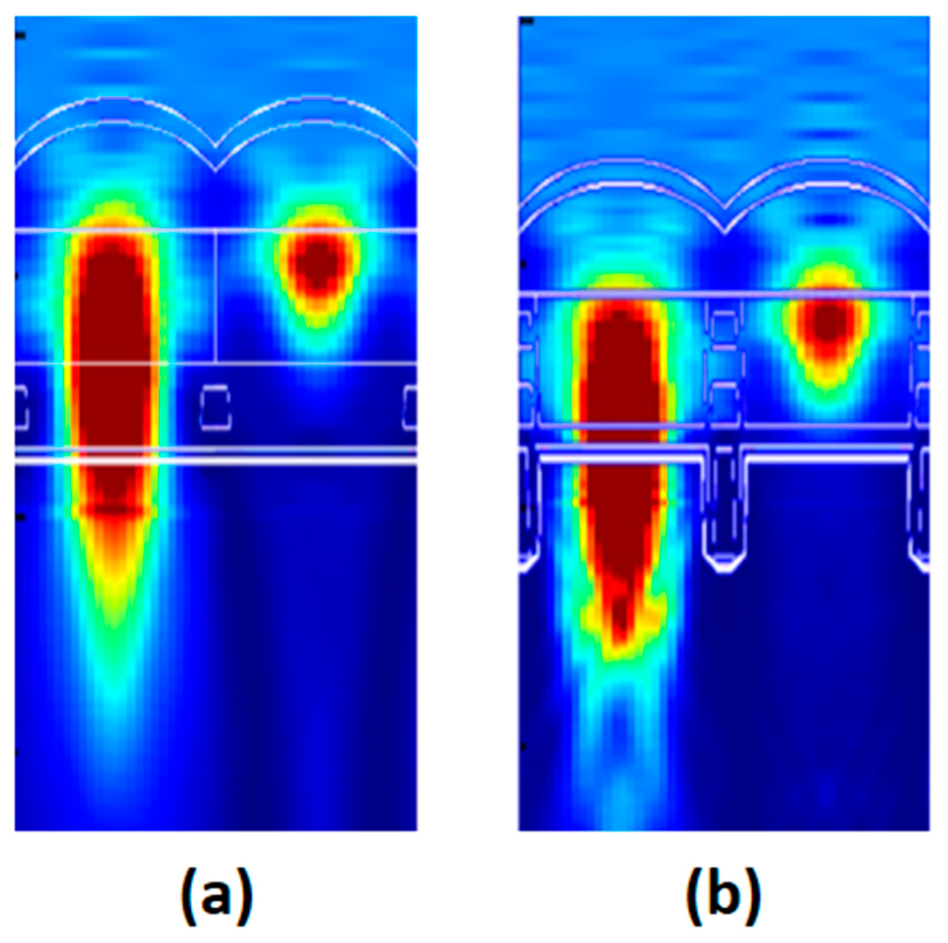
3.2. Low Dark Current Pixel
Another process integration challenge in the submicron pixel is the dark current reduction. Unlike logic transistors, an image sensor basically follows a constant voltage scaling law []. In the constant voltage scaling law, let K be a scaling factor which is greater than 1, doping concentration is proportional to K squared, and electric field is proportional to K. Figure 6 shows the necessary photodiode doping concentration. As expected, a smaller pixel requires a higher photodiode dosage, and a higher ion implant dosage induces more higher ion implant damage in bulk silicon, in addition to a higher electric field.
Figure 6.
Pixel generation vs. the photodiode implant dose.
Dark current and white pixels are functions of defect density and electric field, so reducing these is fundamental.
It is well known that defect located at the transfer gate edge is a main source of dark current and white pixels (Figure 7) []. Concerning defect density reduction, key process conditions such as ion implantation and annealing steps were carefully optimized to minimize every kind of defect and to recover damages.
Figure 7.
Dark current sources marked by “X” and pixel biases.
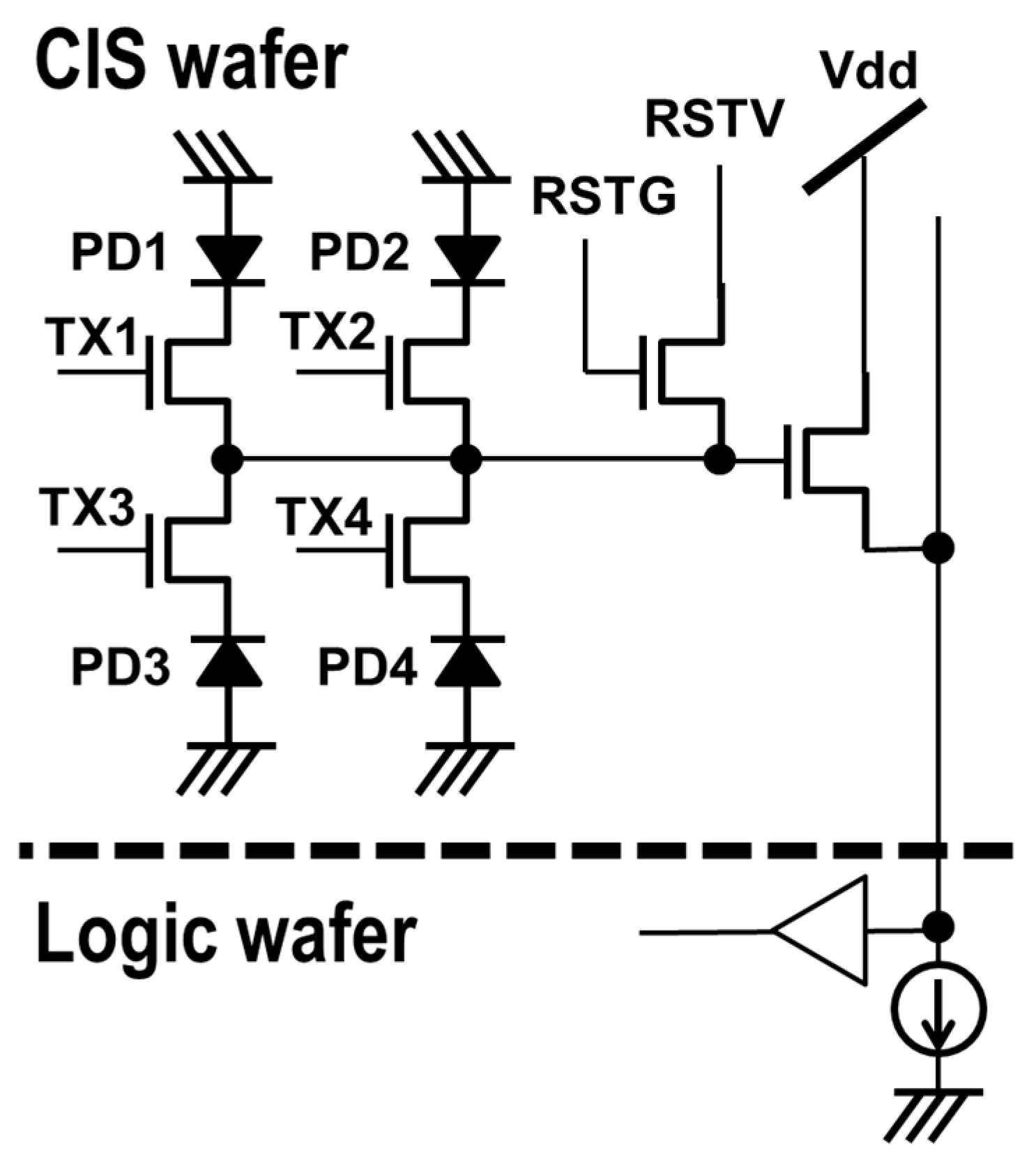
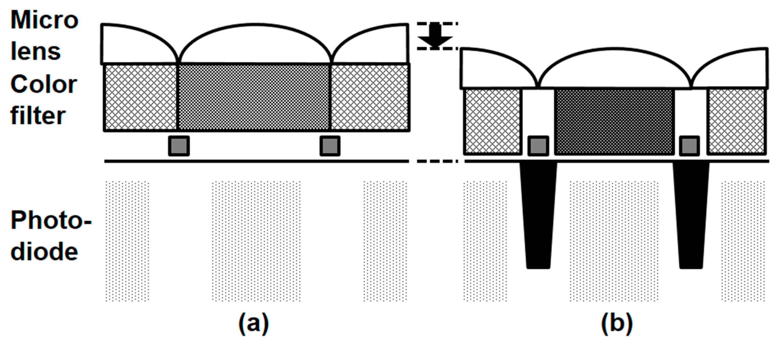
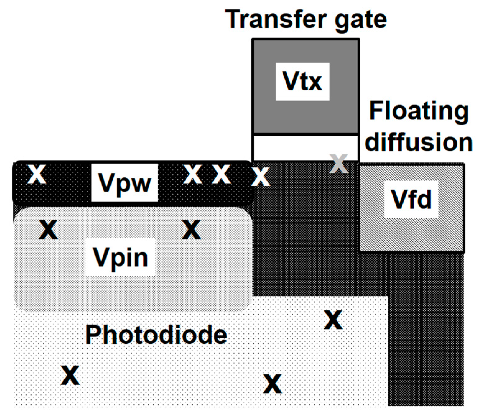
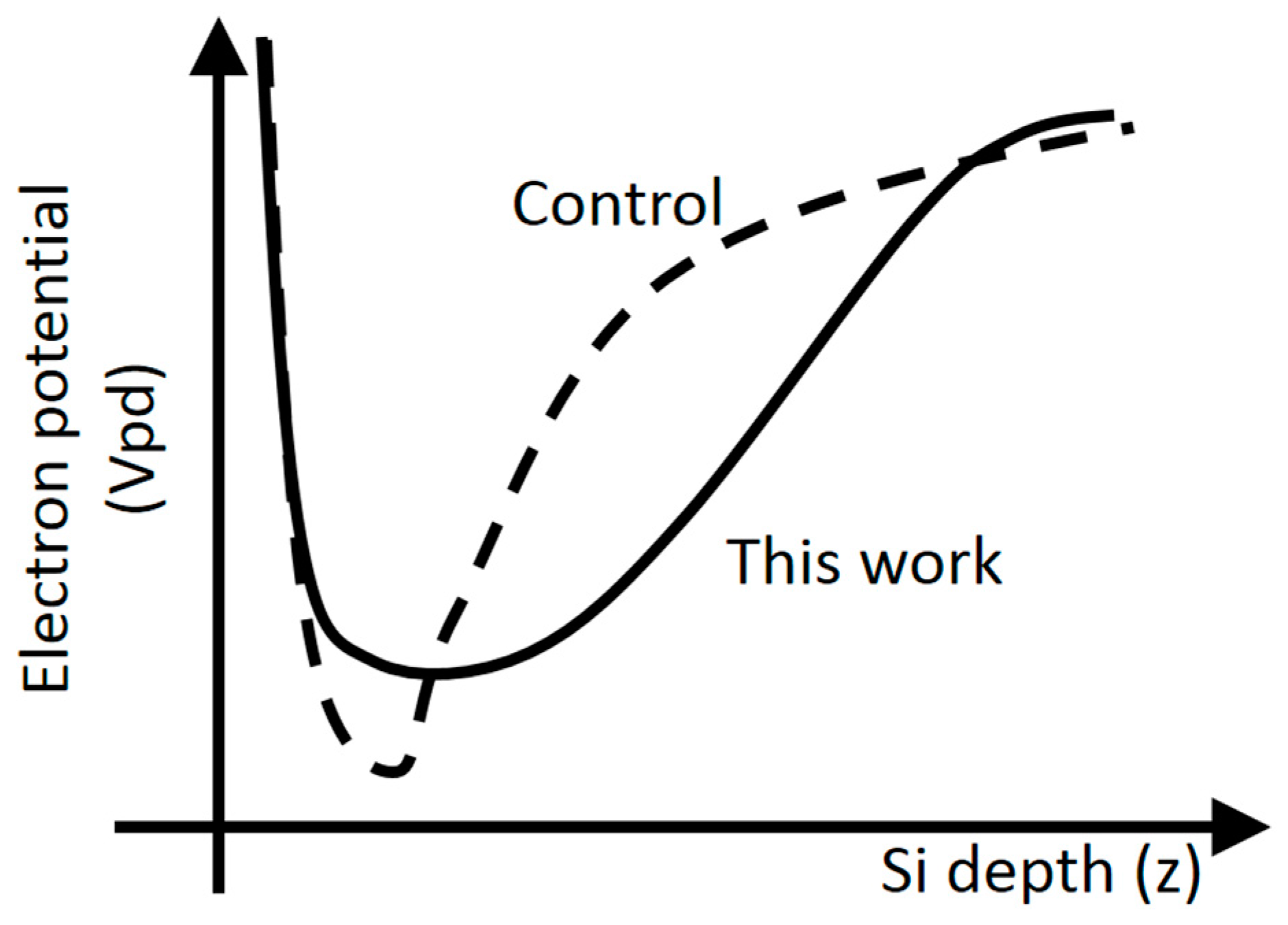
3.3. Pixel Design and Low Dark Current Pixel
The electric field is decreased by device engineering. Reducing floating diffusion node bias (Vfd) works to reduce dark current due to electric field relaxation. However, this degrades anti-blooming due to a lower overflow potential [,]. Therefore, a new pixel structure was developed.
An additional N-type layer was interposed between a shallow photodiode (PD) and a deep photodiode, which also extended to the floating diffusion region (Figure 8). The floating diffusion node bias can be decreased by increasing the additional N-type layer dosage, and anti-blooming performance is not affected.
Figure 8.
Schematic drawing of pixel design concept.
This additional n-type layer is adequate to improve image lag as well. Thanks to the larger image lag margin, by utilizing a deep silicon area as charge storage, the pinning voltage (Vpin) of the photodiode can be decreased while the same FWC is maintained, as shown in Figure 9. Lower pinning voltage also works to reduce dark current.
Figure 9.
Photodiode potential profile. Dashed line is based on control pixel, and solid line is based on the pixel in this experiment.
As shown in Figure 10, it is evident from the three-dimensional technology computer aided design (TCAD) device simulation results that an anti-blooming path was clearly made, and charge transfer capability improved as well.
Figure 10.
3D TCAD simulations of the transfer device structure showing electrostatic potential contours. (a) The control pixel during the integration phase; (b) the pixel in this experiment during the integration phase; (c) the control pixel during the read out phase; (d) the pixel in this experiment during the read out phase.
A histogram of the individual pixel dark current at 60 °C is shown in Figure 11. The dark current peak at 60 °C corresponds to 3.2 e−/s for the 0.9 μm pixel, and the dark current distribution of the 0.9 μm pixel is close to that of the 1.1 μm pixel in spite of the higher photodiode dose.
Figure 11.
Dark current histograms at 60 °C of the 0.9 μm pixel and the 1.1 μm pixel. The gray color indicates the 1.1 μm pixel, and the black color indicates the 0.9 μm pixel.
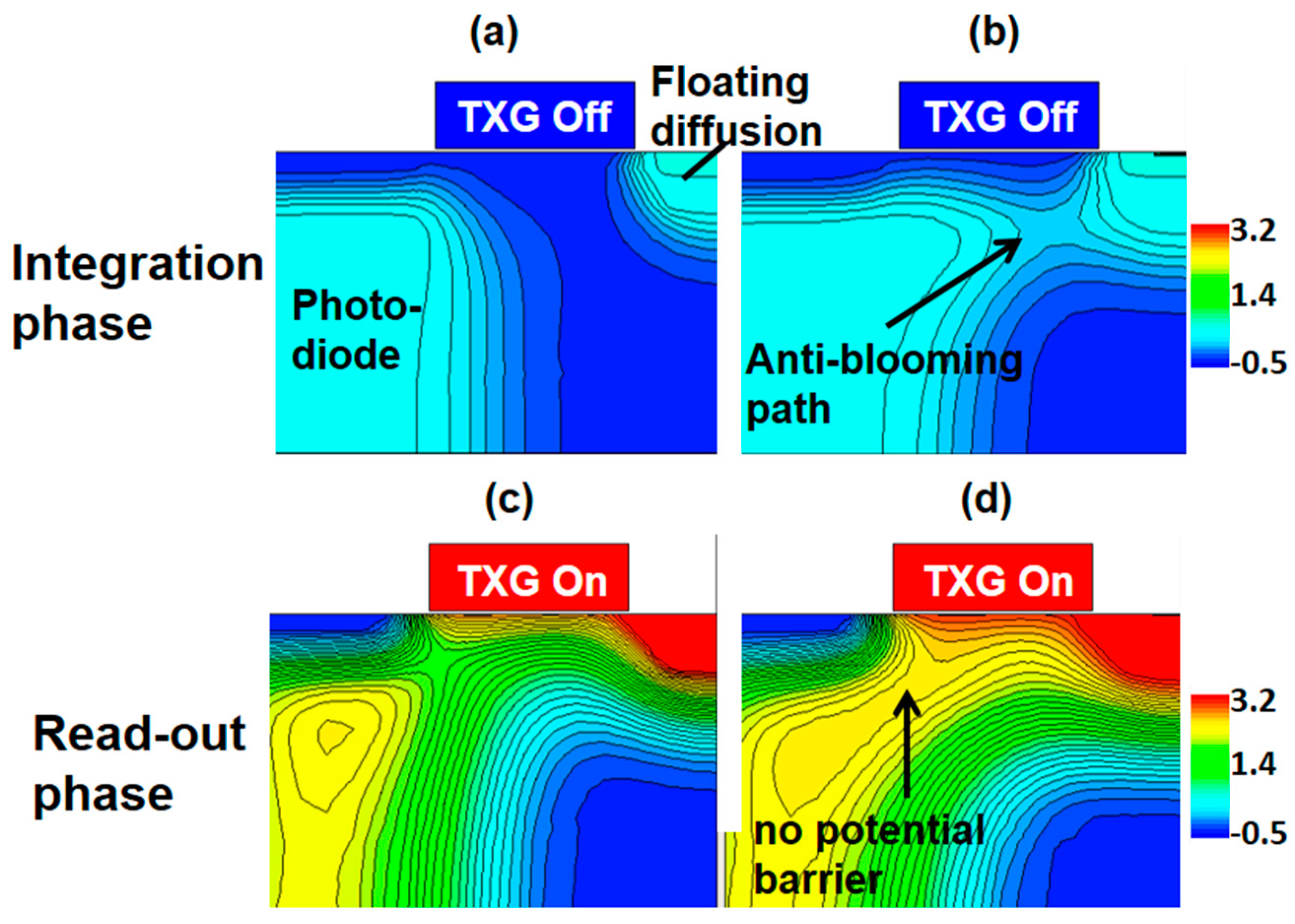
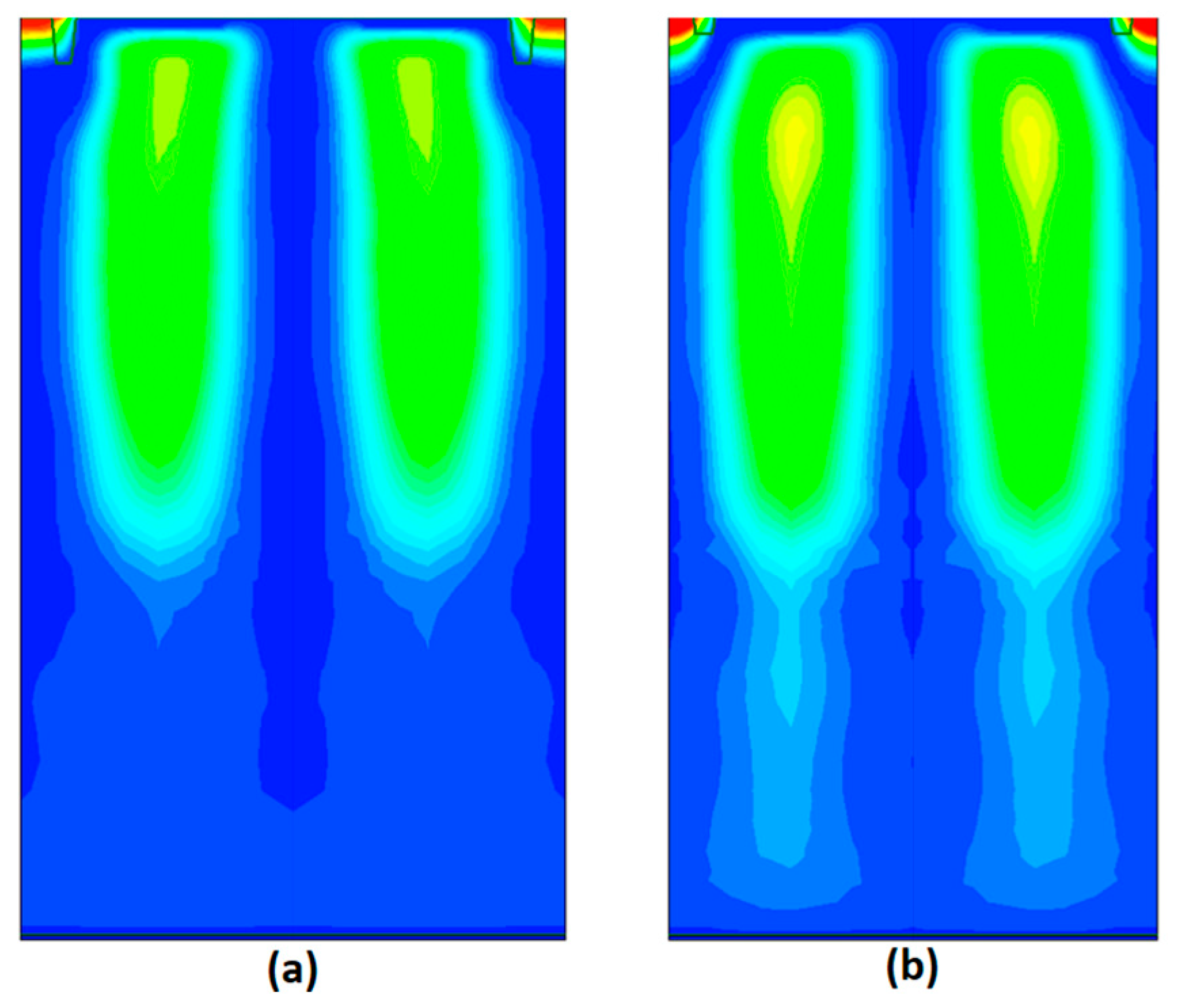
3.4. Anti-Blooming Pixel
Figure 12 shows a light response curve of 0.9 μm pixels. The green color is the green channel, and red is the red channel, and blue is the blue channel. As the TCAD device simulation results show, even after the green channel signal saturated, the adjacent channels, the red and blue signals, were not distorted. From this fact we can conclude that blooming was 0.5% []. This data also shows a measured linear FWC of 4100 e−.
Figure 12.
Light response curve of the 0.9 μm pixel.
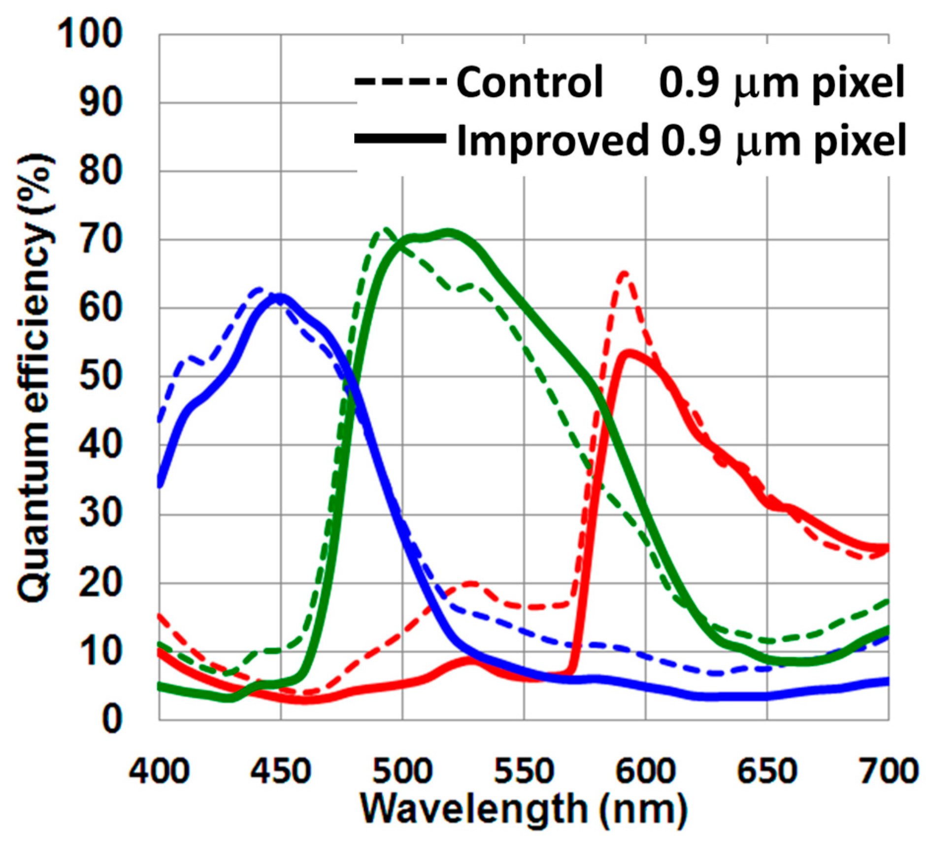
3.5. Low Crosstalk Pixel
Optical crosstalk improvement is mandatory in submicron small pixels [], so we developed optical stack thinning and cross talk suppression techniques. Figure 13 shows a cross-sectional view of the pixel in the backside portion. The optical stack height, defined by the distance between the backside silicon surface and the top of the micro lens, decreased by 10%. Deep trench isolation (DTI) technology was developed to suppress optical crosstalk without sacrificing dark performance in parallel. In addition, a new color filter material was used to improve the SNR10 index.
Figure 13.
Schematic cross-sectional views of pixel. (a) Control pixel; (b) crosstalk-improved pixel.
In order to design an optical structure, we performed a three-dimensional finite difference time domain optical simulation. Based on the optical simulation, a deep trench isolation structure and material, as well as the curvature of the micro-lens, were determined. Figure 14 shows the optical simulation results. The simulation result of the improved pixel exhibits greater light-gathering capability.
Figure 14.
Optical simulation results at an incident wavelength of 530 nm. (a) Control pixel; (b) crosstalk-improved pixel.
Taking into account the optical simulation study results, we made a silicon sample. Obtained quantum efficiency (QE) spectra of the 0.9 μm pixels are shown in Figure 15. Optical crosstalk was greatly suppressed, and the blue and red responses slightly decreased due to a slightly smaller aperture area of the grid structure. Improving the green channel’s quantum efficiency is realized by a newly developed color filter material.
Figure 15.
Measured quantum efficiency spectra of 0.9 μm pixels. Dashed line is the control 0.9 μm pixel, and the solid line is the improved 0.9 μm pixel.
A sample color image taken with the 0.9 μm pixel in the 45 nm stacked CIS process technology is shown in Figure 16. There was no dead line, nor any defects, so this process is robust. Table 2 gives a summary of pixel performance. The process technology consists in 45 nm 1-poly 4-metal (1P4M) stacked CIS. The pixel supply voltage was 2.8 V. Image lag was less than 1 e. Photo response non-uniformity was 0.90%, and the QE at the green peak was 71%.
Figure 16.
A sample color image taken with the 0.9 μm pixel manufactured in the 45 nm stacked CIS.
Table 2.
Sensor characteristics of the 0.9 μm pixel.
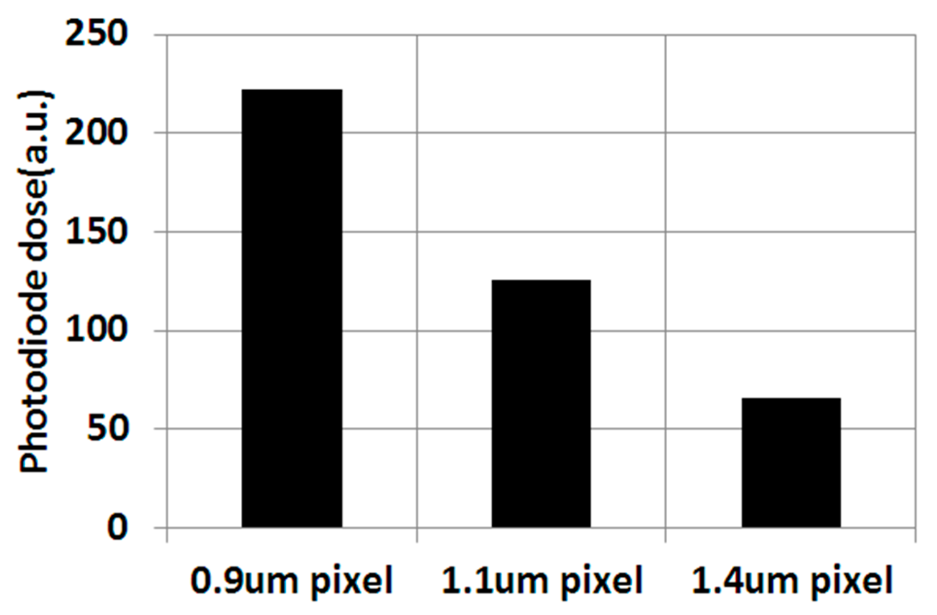
4. 0.8 μm Pixel Generation
The 0.9 μm pixel performance met market requirements, so we then decided to study 0.8 μm pixel generation. Assuming a 0.8 μm pixel uses a similar pixel structure and architecture, we estimated the performance by simulation and calculation.
First, we considered pixel noise and pixel RTN. Regarding RTN, source follower channel length is a key factor, and the length should be greater than 0.5 μm to efficiently suppress RTN []. Our pixel layout study confirmed that a more advanced node technology can provide a source follower device with a channel length greater than 0.5 μm in 0.8 μm pixels.
The optical cross-talk problem can be improved by deepening the DTI. In addition, a further thinning down of the optical stack height is still effective.
The most serious problem is still a low FWC. If the pixel size shrinks down from 0.9 to 0.8 μm based on the same process technology, FWC will be about 2800 e−, and photon noise will limit the image quality []. To maintain a reasonable image quality, the FWC needs at least 3000 e−. A simplified form of FWC can be expressed as
where z is the silicon depth, Cpd(z) and Vpd(z) are the photodiode capacitance at a silicon depth of z and the depleted photodiode potential at a silicon depth of z, respectively, and Vovf is the overflow potential.
Vovf is determined to fulfill anti-blooming criterion and cannot be changed. Cpd(z) can be increased by tightening the pixel-to-pixel isolation design rule. The simulated FWC with a tighter design rule then increases from 2800 to 3500 e−, rendering the quality of an image possibly acceptable. Comparisons between 0.9 μm pixel and 0.8 μm pixel can be made by studying Figure 17, in which the 0.8 μm pixel shows narrower pixel-to-pixel isolation.
Figure 17.
Three-dimensional TCAD simulations of photodiode showing electrostatic potential contours. (a) Two 0.9 μm pixels; (b) two 0.8 μm pixels.
Further improvement can be made by designing a vertically extended photodiode potential structure, or by simply increasing the pixel supply voltage, which would allow for the use of a higher Vpd(z). It should be noted that the suppression of dark current and white pixel caused by a higher electric field in a photodiode must be taken into account.
5. Conclusions
The 45 nm advanced technology is desirable for submicron pixel generation due to tighter design rules and higher controllability for process variation. In addition, the flexibility of the stacked CIS process improves pixel performance. A novel 0.9 μm pixel with well-balanced light and dark performances, making full use of a highly manufacturable 45 nm advanced technology with a stacked CIS, is presented here. A low dark current of 3.2 e−/s at 60 °C, an ultra-low read noise of 0.90 e−·rms, a high FWC of 4100 e−, and blooming of 0.5% are demonstrated in a 0.9 μm pixel with a pixel supply voltage of 2.8 V. A simulation study of 0.8 μm pixel indicates that more advanced node technology with tightened pixel design rules lead to acceptable pixel performances. This technology offers image sensors a high resolution, superior low light imaging, and small chip size features.
Author Contributions
Seiji Takahashi designed pixels, designed experiments, analyzed data, characterized pixels, and wrote the manuscript. Yi-Min Huang, Jhy-Jyi Sze, Tung-Ting Wu, Fu-Sheng Guo, Wei-Cheng Hsu, Tung-Hsiung Tseng, King Liao, Chin-Chia Kuo, Tzu-Hsiang Chen, Chuan-Joung Wang, and Dun-Nien Yaung developed special process modules, integrated new and improved process workflow, optimized the process, and performed device fabrications. Wei-Chieh Chiang, Chun-Hao Chuang, Keng-Yu Chou, and Chien-Hsien Tseng performed optical design. Chi-Hsien Chung and Chun-Hao Chuang performed the pixel characterization. Kuo-Yu Chou designed the peripheral circuit.
Conflicts of Interest
The authors declare no conflict of interest.
References
- Fossum, E.R. What to do with sub-diffraction-limit (SDL) pixels?—A proposal for a gigapixel digital film sensor (DFS). In Proceedings of the IEEE Workshop on Charge-Coupled Devices and Advanced Image Sensors, Nagano, Japan, 8–11 June 2005; pp. 214–217. [Google Scholar]
- Jung, Y.J. Enhancement of low light level images using color-plus-mono dual camera. Opt. Express 2017, 25, 12029–12051. [Google Scholar] [CrossRef] [PubMed]
- Kobayashi, M.; Johnson, M.; Wada, Y.; Tsuboi, H.; Ono, T.; Takada, H.; Togo, K.; Kishi, T.; Takahashi, H.; Ichikawa, T.; et al. A Low Noise and High Sensitivity Image Sensor with Imaging and Phase-Difference Detection AF in All Pixels. ITE Trans. Media Technol. Appl. 2016, 4, 123–128. [Google Scholar] [CrossRef]
- Ahn, J.C.; Moon, C.R.; Kim, B.; Lee, K.; Kim, Y.; Lim, M.; Lee, W.; Park, H.; Moon, K.; Yoo, J.; et al. Advanced image sensor technology for pixel scaling down toward 1.0 µm (Invited). In Proceedings of the IEEE International Electron Devices Meeting, San Francisco, CA, USA, 15–17 December 2008; pp. 1–4. [Google Scholar]
- Wuu, S.G.; Wang, C.C.; Hsieh, B.C.; Tu, Y.L.; Tseng, C.H.; Hsu, T.H.; Hsiao, R.S.; Takahashi, S.; Lin, R.J.; Tsai, C.S.; et al. A leading-edge 0.9 µm pixel CMOS image sensor technology with backside illumination: Future challenges for pixel scaling. In Proceedings of the IEEE International Electron Devices Meeting, San Francisco, CA, USA, 6–8 December 2010. [Google Scholar]
- Yaung, D.N.; Hsieh, B.C.; Wang, C.C.; Liu, J.C.; Wang, T.J.; Wang, W.D.; Chuang, C.C.; Chao, C.; Tu, Y.L.; Tsai, C.S.; et al. High performance 300 mm backside illumination technology for continuous pixel shrinkage. In Proceedings of the IEEE International Electron Devices Meeting, Washington, DC, USA, 5–7 December 2011. [Google Scholar]
- Sukegawa, S.; Umebayashi, T.; Nakajima, T.; Kawanobe, H.; Koseki, K.; Hirota, I.; Haruta, T.; Kasai, M.; Fukumoto, K.; Wakano, T.; et al. A 1/4-inch 8 Mpixel back-illuminated stacked CMOS image sensor. In Proceedings of the IEEE International Solid-State Circuits Conference Digest of Technical Papers (ISSCC), San Francisco, CA, USA, 17–21 February 2013. [Google Scholar]
- Cheng, K.L.; Wu, C.C.; Wang, Y.P.; Lin, D.W.; Chu, C.M.; Tarng, Y.Y.; Lu, S.Y.; Yang, S.J.; Hsieh, M.H.; Liu, C.M.; et al. A Highly Scaled, High Performance 45 nm Bulk Logic CMOS Technology with 0.242 µm2 SRAM Cell. In Proceedings of the IEEE International Electron Devices Meeting, Washington, DC, USA, 10–12 December 2007; pp. 243–246. [Google Scholar]
- Takahashi, S.; Huang, Y.-M.; Sze, J.-J.; Wu, T.-T.; Guo, F.-S.; Hsu, W.-C.; Tseng, T.-H.; Liao, K.; Kuo, C.-C.; Chen, T.-H.; et al. Low Dark Current and Low Noise 0.9 µm Pixel in a 45 nm Stacked CMOS Image Sensor Process Technology. In Proceedings of the 2017 International Image Sensor Workshop, Hiroshima, Japan, 30 May–2 June 2017. [Google Scholar]
- Liu, J.C.; Yaung, D.N.; Sze, J.J.; Wang, C.C.; Hung, G.; Wang, C.J.; Hsu, T.H.; Lin, R.J.; Wang, T.J.; Wang, W.D.; et al. Advanced 1.1 µm Pixel CMOS Image Sensor with 3D Stacked Architecture. In Proceedings of the 2014 Symposium on VLSI Technology (VLSI-Technology): Digest of Technical Papers, Honolulu, HI, USA, 9–12 June 2014. [Google Scholar]
- Nakamura, J. Image Sensors and Signal Processing for Digital Still Cameras, 1st ed.; CRC Press: Boca Raton, FL, USA, 2006. [Google Scholar]
- Abe, K.; Sugawa, S.; Kuroda, R.; Watabe, S.; Miyamoto, N.; Teramoto, A.; Ohmi, T.; Kamata, Y.; Shibusawa, K. Analysis of Source Follower Random Telegraph Signal Using nMOS and pMOS Array TEG. In Proceedings of the International Image Sensor Workshop, Hiroshima, Japan, 30 May–2 June 2017; pp. 62–65. [Google Scholar]
- Jantsch, O. Flicker (1/f) noise generated by a random walk of electrons in interfaces. IEEE Trans. Electron Devices 1987, 34, 1100–1115. [Google Scholar] [CrossRef]
- Sze, J.J.; Lin, R.J.; Takahashi, S.; Hung, J.M.; Lu, Y.C.; Tseng, T.H.; Wang, C.C.; Ting, S.F.; Wuu, S.G. The Impact of Gate Edge Damage on Pixel Read Noise. In Proceedings of the International Image Sensor Workshop, Snowbird, UT, USA, 12–16 June 2013. [Google Scholar]
- Taure, Y.; Ning, T.H. Fundamentals of Modern VLSI Devices; Cambridge University Press: Cambridge, UK, 1998. [Google Scholar]
- Watanabe, T.; Park, J.H.; Aoyama, S.; Isobe, K.; Kawahito, S. Effects of Negative-Bias Operation and Optical Stress on Dark Current in CMOS Image Sensors. IEEE Trans. Electron Devices 2010, 57, 1512–1518. [Google Scholar] [CrossRef]
- Sequin, C.H.; Shankoff, T.A.; Sealer, D.A. Measurements on a charge-coupled area image sensor with blooming suppression. IEEE Trans. Electron Devices 1974, 21, 331–341. [Google Scholar] [CrossRef]
- Adachi, S.; Simada, H.; Gotoh, H.; Mizobuchi, K. A novel lateral overflow drain technology for high quantum efficiency CCD imagers. In Proceedings of the IEEE International Electron Devices Meeting, San Francisco, CA, USA, 10–13 December 2000. [Google Scholar]
- Chao, C.; Chou, K.Y.; Liu, C.; Chen, Y.C.; Tu, H.Y.; Cheng, H.Y.; Hsueh, F.L.; Wuu, S.G. Blooming and Antiblooming in 1.1 µm-Pixel CIS. In Proceedings of the International Image Sensor Workshop, Snowbird, UT, USA, 12–16 June 2013. [Google Scholar]
- Kitamura, Y.; Aikawa, H.; Kakehi, K.; Yousyou, T.; Eda, K.; Minami, T.; Uya, S.; Takegawa, Y.; Yamashita, H.; Kohyama, Y.; et al. Suppression of Crosstalk by Using Backside Deep Trench Isolation for 1.12 μm Backside Illuminated CMOS Image Sensor. In Proceedings of the IEEE International Electron Devices Meeting, San Francisco, CA, USA, 10–13 December 2012. [Google Scholar]
- Catrysse, P.B.; Wandell, B.A. Roadmap for CMOS image sensors: Moore meets Planck and Sommerfeld. SPIE 2005, 5678, 1–13. [Google Scholar]
© 2017 by the authors. Licensee MDPI, Basel, Switzerland. This article is an open access article distributed under the terms and conditions of the Creative Commons Attribution (CC BY) license (http://creativecommons.org/licenses/by/4.0/).