A Wireless Passive Pressure Microsensor Fabricated in HTCC MEMS Technology for Harsh Environments

 ,
,
Abstract
: A wireless passive high-temperature pressure sensor without evacuation channel fabricated in high-temperature co-fired ceramics (HTCC) technology is proposed. The properties of the HTCC material ensure the sensor can be applied in harsh environments. The sensor without evacuation channel can be completely gastight. The wireless data is obtained with a reader antenna by mutual inductance coupling. Experimental systems are designed to obtain the frequency-pressure characteristic, frequency-temperature characteristic and coupling distance. Experimental results show that the sensor can be coupled with an antenna at 600 °C and max distance of 2.8 cm at room temperature. The senor sensitivity is about 860 Hz/bar and hysteresis error and repeatability error are quite low.1. Introduction
Nowadays, high temperature pressure sensors has been attached great importance due to their excellent work capability in harsh temperature environments such as in automobiles [1], aero engine turbines [2], aeronautics [3] and is one of the important areas in the sensor research [4]. High temperature pressure sensors have broad application prospects in the area of civil industry and national defense [5].
With the fast development in the last decades of micromachining technology, micro-electromechanical system (MEMS) sensors are the major devices used in measuring pressure [6]. Most pressure sensors are made from silicon. However, silicon sensors with PN-junctions exhibit a drawback, which is they cannot be used above 150 °C, since the leakage current across the junctions drastically increases at 150 °C [7]. Furthermore, above 500 °C, the mechanical properties of silicon will deteriorate as the material becomes easily deformable when pressure is applied [8]. Using SOI material can increase the operation temperature of sensor, but sensor become invalid because the silicon material will lose elasticity at 500 °C [9,10]. The Georgia Institute of Technology has designed a wireless high temperature pressure sensor using low temperature co-fired ceramic (LTCC) material. However, the sensor is only tested to 450 °C [11–14]. Another team in Novi Sad (Serbia) demonstrated in 2009 a better structure, but worse performance [15,16]. Two LTCC layers are added above the metal electrode to provide perfect protection, but the sensor sensitivity is only 25.6 kHz/bar. Xiong, et al. [17] have showed the measurement and fabrication of wireless pressure sensor fabricated in HTCC MEMS technology, but the sensor has not been tested in high temperature environments. Recently Jie Yang has introduced a harsh environment wireless pressure sensing solution utilizing high temperature electronics; the proposed approach was verified through prototype fabrication and high temperature bench testing from room temperature up to 450 °C [18].
A pressure sensor based on HTCC technology is proposed. The non-contact measurement technology and HTCC material are involved to solve the problem of lead degradation and elastic properties deterioration of materials at ultra-high temperature, respectively [19].The sensor in this article does not have evacuation channel and exit hole in order to ensure the sensor is completely gastight in harsh environments. The wireless resonant sensor is based on an LC circuit. By using this signal extraction method, the sensor has great potential for enlarging the working temperature range and a great advantage in miniaturization and its self-adaptive package [20].
A precision frequency-pressure characteristic measurement system is built to measure the sensor resonant frequency at room temperature. The sensor resonant frequency is read by extracting the impedance phase dependences of the antenna coil. Furthermore, the sensor frequency-temperature characteristic and coupling distance have been measured with high temperature measurement system and coupling distance testing platform, respectively.
2. Sensor Design
The sensor designed in this paper can be equal to a series LC resonant circuit which consists of variable capacitance and invariable inductance, and is powered by a reader antenna [21]. The resonant frequency can be retrieved from the expression:
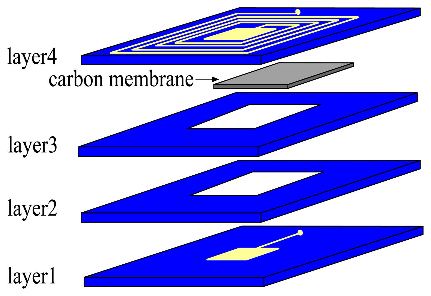
The cross section of sensor model which consists of four green tapes is shown in Figure 1. The inductor is designed as a square spiral type and placed on the layer 4. Relevant geometrical parameters of the inductor are given in Table 1. The capacitor is a parallel plate type with square electrodes. The lower capacitor electrode is placed on the top side of the layer 1, while the upper electrode resides on the top side of the layer 4. The relevant geometrical parameters of the capacitor are given in Table 2. An air-gap is present between the two capacitor electrodes. Electrical connection between capacitor plates and inductor is realized with metalized via.
Tape layers with the capacitor electrodes act as sensor membranes which react to pressure. The sensor presented in this paper does not have an evacuation channel in order to ensure the sensor is completely gastight. The carbon membrane which prevents collapse of cavity during lamination will become carbon dioxide during co-firing and spread to air through the small pores which are formed after volatilization of organics. Characteristics of the implemented tape are shown in Table 3.
3. Model Analysis
The variations of pressure signal are detected by changes in the sensors' capacitance as shown in Figure 2. When the sensor has been fabricated, the pressure in cavity is about 0.166 atm, which is smaller than the outside pressure of 1 atm. It means that the pressure of 0.834 atm is initially applied on the membrane, so the initial square parallel capacitance can be determined as [23]:
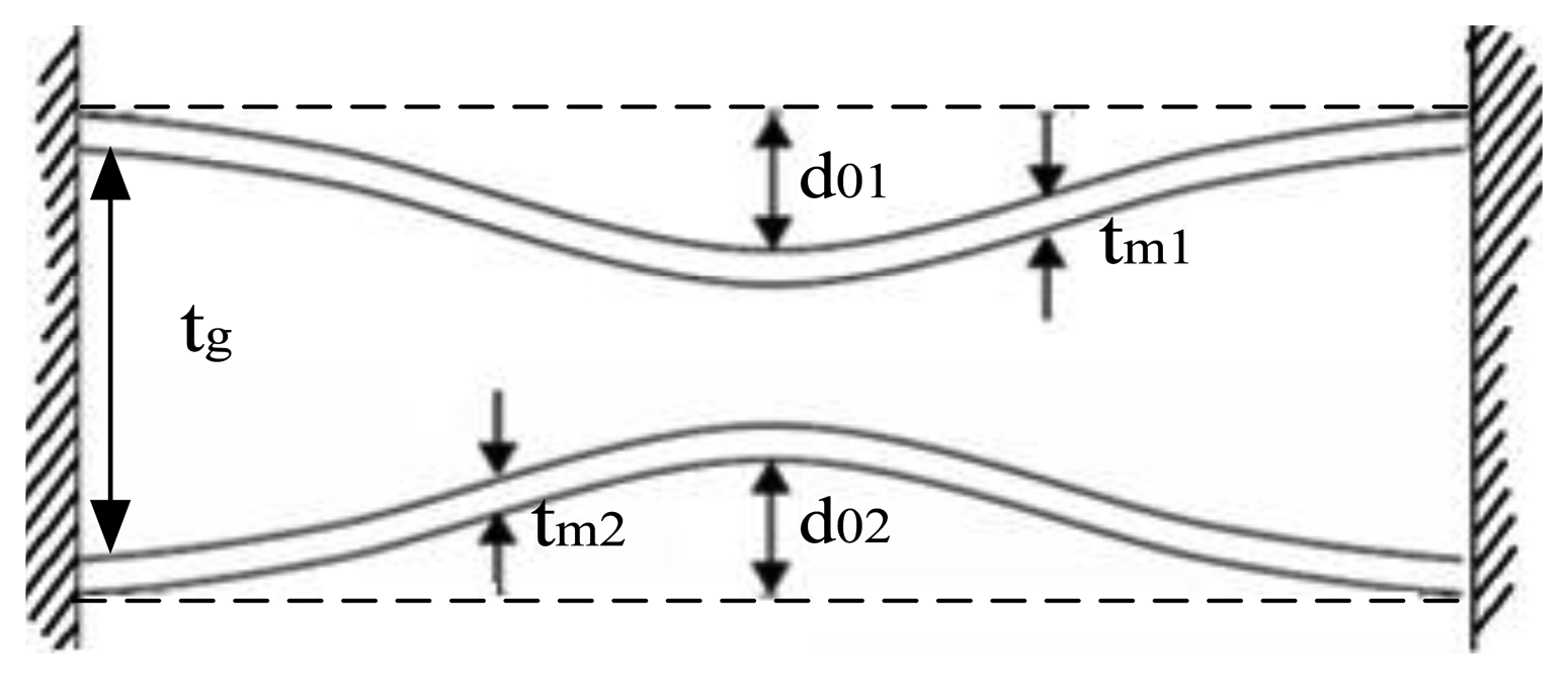
The membrane is deformed when pressure is applied, which is shown schematically in Figure 3. When pressure is applied on membranes, the sensor capacitance can be derived using the expression:
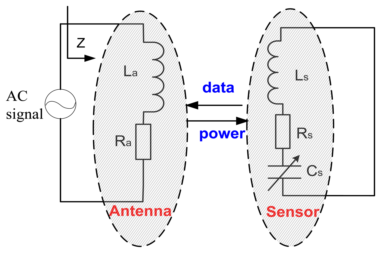
A wireless measurement technique is provided for data retrieval [25]. The electrical model of the sensor-antenna system is presented in Figure 4 [26].
The alternating signal which is input through the sweeping frequency at the signal test end is sent out to the inductance coil of sensor in the form of electromagnetic energy by the reader antenna coil. When the signal frequency is equal to the sensor resonance frequency, the input impedance of antenna will change apparently [27]. The sensor resonant frequency can be obtained through testing antenna impedance phase with Agilent the E4991A Impedance Analyzer. The total impedance of the reader antenna can be determined as:
4. Fabrication
The sensor is fabricated in HTCC technology which covers more than 10 processes include milling, tape casting, cutting, hole drilling, screen-printing, stacking, isostatic lamination, firing, etc. [28]. Part of THE fabrication process is shown in Figure 5.
The first step is to cut THE via and cavity using a drill. Then the screen-printing technique is applied for printing of metal figure and via filling. Platinum paste is used for metallization printing and via filling and its properties are shown in Table 4. Afterwards, the printed tapes are put in a furnace for 20 min at 100 °C. The next process is to stack Section 1, include layer 1, layer 2 and layer 3 and placing of carbon membrane in the cavity. After that, stack layer 4 is applied on Section 1.
Isostatic lamination of the HTCC layers has been performed at a pressure of 15 MPa and temperature of 75 °C for 20 min after vacuum packaging. The laminated stack is sintered in a furnace and heated 430 °C (1 °C/min ramp rate) in air and heated 600 °C (2 °C/min ramp rate) and then for 126 min at a peak temperature of 1,512 °C (12.5 °C/min ramp rate). The geometrical parameters of the sensor design after fabrication is shown in Table 5.
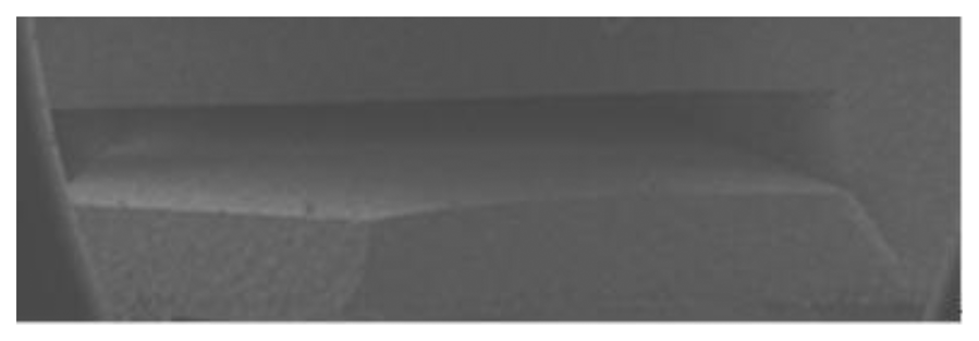
The cavity formation is shown in Figure 6. Organics in the substrate decompose severely at 100–360 °C in the sintering process; the decomposition of organics in the substrate includes two processes [29]: removal of volatile organic and volatile product. The first stage refers to the volatilization of organic solvents and the removal of plasticizer and other small molecule organics. The organics can spread to the surface of the HTCC tape, and then diffuse to air due to the sufficient vapor pressure in HTCC tape. The second stage is that volatile decomposition products are produced constantly during the process of thermal decomposition and spread to the surface to air. Then the pores are formed after decomposition of organics in substrate. The carbon membrane turns into CO2 at about 600 °C and spreads to air through the pores. CO2 can also spread to air thru the pores which is covered by the electrode because the ceramic tape and platinum paste are not impermeable at 600 °C. The green tape will be impermeable after a full sintering process. SEM analysis of cavity is presented in Figure 7. As can be seen in Figure 7, the cavity is preserved well.
5. Experiments
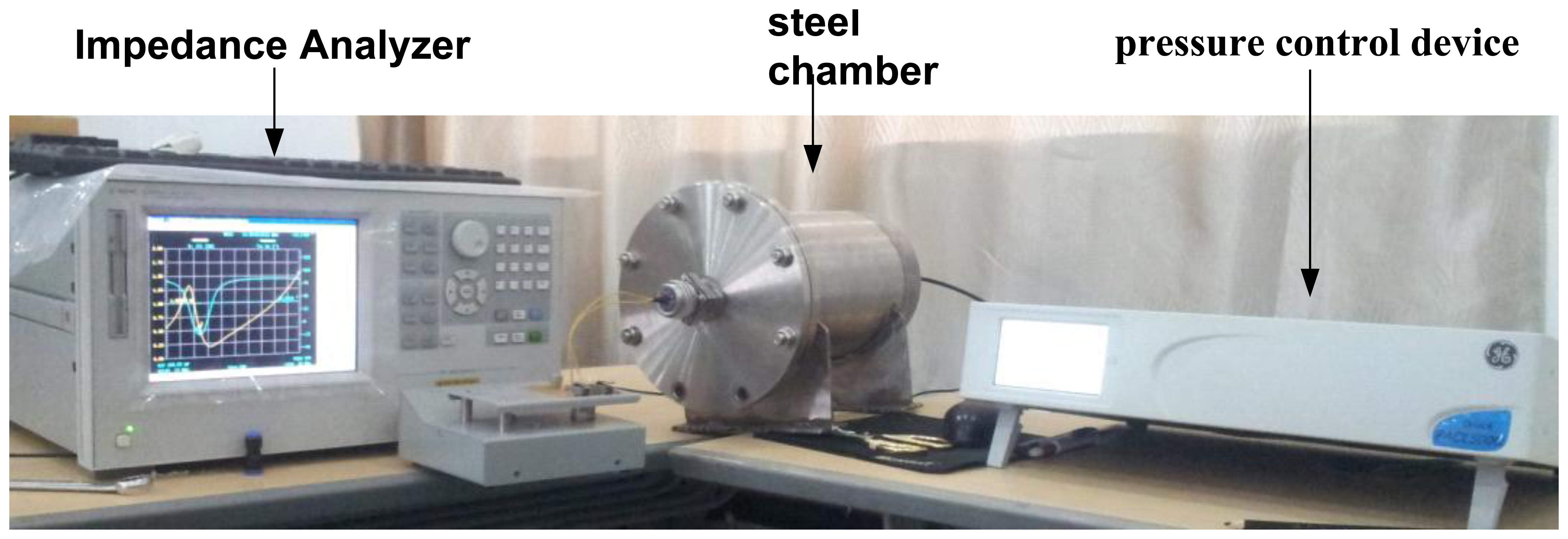
A frequency-pressure measurement system which consists of an Agilent E4991A Impedance Analyzer, steel chamber, pressure control device and nitrogen pressure tank as shown in Figure 8 is designed in order to measure the sensor resonant frequency at different pressures at room temperature. The antenna and sensor are a certain distance apart without any electric connection inside the chamber.
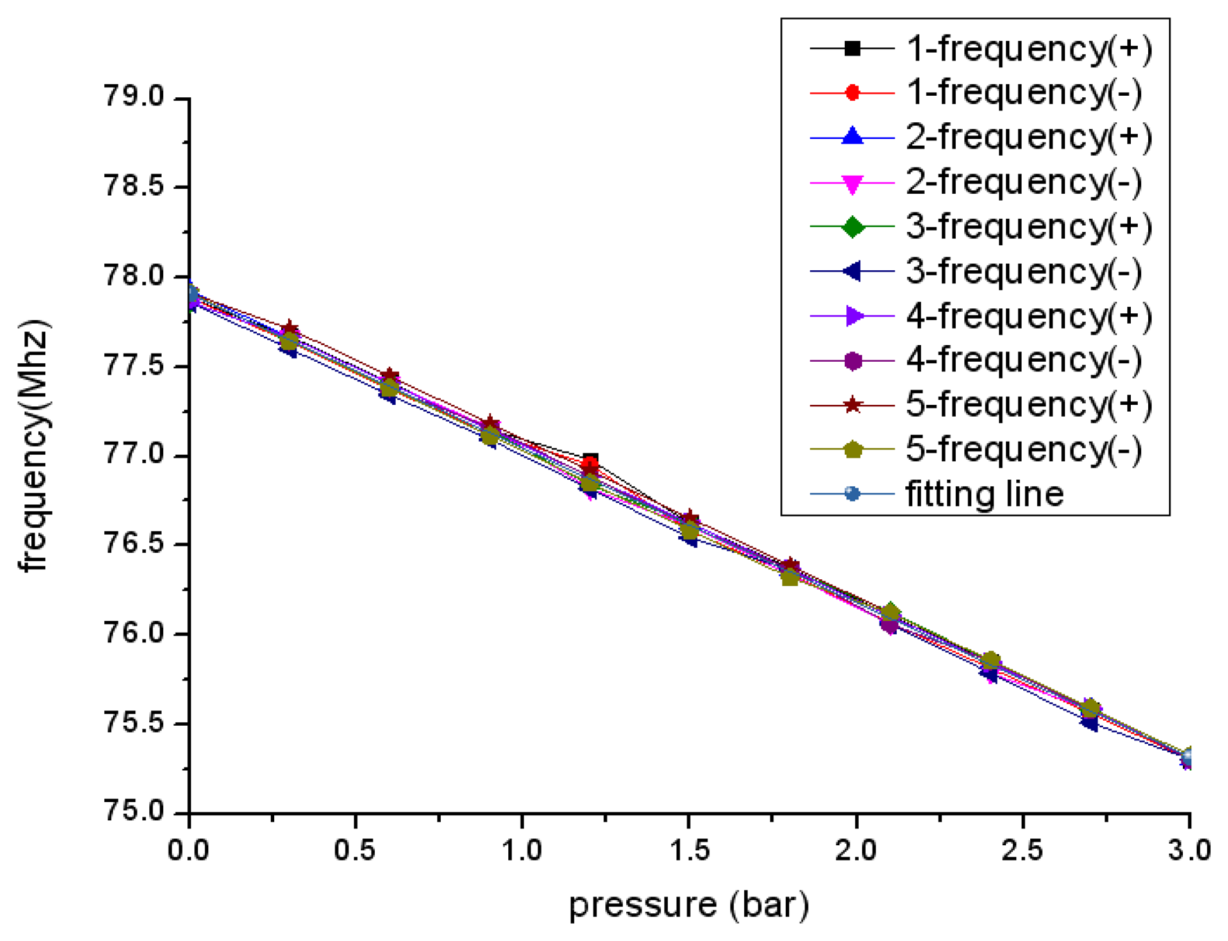
The sensor output signal has been measured in the form of positive route and reverse route five times respectively. The measured sensor characteristic is shown in Figure 9. As can be seen, the change of sensor resonant frequency dependence on pressure approximates a linear variation.
The linearity, hysteresis error, repeatability error of sensor can be determined as:
The linearity δL, hysteresis error δH and repeatability error δR are 96.56%, 3.12% and 6.03%, respectively. The sensor resonant frequency at zero pressure is 77.76 MHz, which is larger than the calculated value. This is expected because the dimensions of metallization and green tape become small after sintering. Specifically, the inductance becomes small because the dimensions of inductance become small. Both of capacitor electrodes area and distance between electrodes become small, however decrease of capacitor electrodes area makes more contribution, finally the capacitor becomes small. The frequency calculated using dimensions after fabrication is still smaller than the measured value and the reason can be obtained from the Equation (6):
The sensor has been tested as a function of temperature from 25 °C to 600 °C with the high temperature measurement system consisting of a muffle furnace and impedance analyzer shown in Figure 11. The antenna measured at high temperature is coiled tungsten wire due to its better stability at high temperature. The antenna and sensor are measured in the muffle furnace and impedance analyzer is in the room temperature environment.
From the measurement results shown in Figure 12 and Figure 13, it is clear that the frequency reduces as the temperature increases and the inductance and parasitic capacitance of the inductance coil change slightly. Therefore, the inductance and parasitic capacitance of the inductance coil have little effect on the decrease of sensor resonance frequency as the temperature increases. Further, the sensor can be coupled with the tungsten antenna at 600 °C, but the coupling effect at 600 °C is impaired apparently compared with at 25 °C, as shown in Figure 14. In order to strengthen the coupling effect and measure the sensor at higher temperatures, the geometry parameter of inductance coil should be optimized.
6. Conclusions
The presented resonant pressure sensor applying standard HTCC technology is realized with a passive LC circuit. The proposed sensor is a good choice for applications in harsh environments because of the excellent properties of the HTCC material in such environments. The sensor presented does not have an evacuation channel, therefore, there is no need to seal the evacuation channel and the sensor is completely gastight in harsh environments. Pressure variations are detected by a change in sensor resonant frequency. The experimental results show that the sensor data can be detected at 600 °C and a maximum distance of 2.8 cm at room temperature. The sensor exhibits an almost linear change of the resonant frequency and a sizable sensitivity. Besides, the nonlinearity, hysteresis error and repeatability error are quite low.
Future work will be directed towards improving the sensitivity of the sensor and enlarge the sensor measurement temperature range by optimizing the geometric parameters of the inductance coil and measuring the temperature characteristics of the electrode capacitance of sensor. Further, by using the green tape with lower Young's modulus and enlarging the electrode area the sensor sensitivity can also be improved.
Acknowledgments
This work was supported by the National Basic Research Program (973) of China (No. 2010CB334703) and the National Natural Science Foundation of China (No. 51075375).
Conflicts of Interest
The author declares no conflict of interest.
References
- Johnson, R.W.; Evans, J.L.; Jacobsen, P.; Thompson, J.R.; Christopher, M. The changing automotive environment: High-temperature electronics. IEEE Trans. Electron. Packag. Manuf. 2004, 27, 164–176. [Google Scholar]
- Gu, Y.; Teng, X.; Liu, C.; He, Y.; Tao, C. Microstructures and ultra-high cycle fatigue behaviors of directionally solidified superalloy DZ125 after Long-term aging. Acta Aeronaut. Astronaut. Sin. 2012, 33, 2136–2142. [Google Scholar]
- George, T.; Son, K.A.; Powers, R.A.; Del Castillo, L.Y.; Okojie, R. Harsh Environment Microtechnologies for NASA and Terrestrial Applications. Proceedings of IEEE, Sensors, Irvine, CA, USA, 30 October 2005; pp. 1253–1258.
- Werner, M.R.; Fahrner, W.R. Review on materials, microsensors, systems and devices for high-temperature and harsh-environment applications. IEEE Trans. Ind. Electron. 2001, 48, 249–257. [Google Scholar]
- Beeby, S.; Ensell, G.; Kraft, M.; White, N. MEMS Mechanical Sensors; Artech House Inc.: Boston, London, UK, 2004. [Google Scholar]
- Eaton, W.P.; Smith, J.H. Micromachined pressure sensors: Review and recent developments. Smart Mater. Struct. 1999, 6, 530–539. [Google Scholar]
- Hase, Y.; Bessho, M.; Ipposhi, T. SOI Type Pressure Sensor for High Temperature Pressure Measurement; Society of Automotive Engineers: New York, NY, USA, 1994. [Google Scholar]
- Eickhoff, M.; Reinhardt, P.; Kroetz, G. Accelerated Aging of Micromachined SiliconrSilicon Carbide Diaphragms by the Application of Pressure and Temperature. Proceedings of the 2nd Conference on Micro Materials, Berlin, Germany, 16–18 April 1997; p. 955.
- Diem, B.; Rey, P.; Renard, S.; Viollet Bosson, S.; Bono, H.; Michel, F.; Delaye, M.T.; Delapierre, G. SOI ‘SIMOX’; from bulk to surface micromachining, a new age for silicon sensors and actuators. Sens. Actuators A: Phys. 1995, 8, 46–47. [Google Scholar]
- Nakamura, T. SOI Technologies for Sensors. Tech. Dig. Transducers 1993, 93, 230–232. [Google Scholar]
- Fonseca, M.A.; English, J.M.; Arx, M.; Allen, M.G. Wireless micromachined ceramic pressure sensor for high-temperature applications. J. Microelectrome-chanical Syst. 2002, 11, 337–343. [Google Scholar]
- English, J.M.; Allen, M.G. Wireless Micromachined Ceramic Pressure Sensors. 21 January 1999; pp. 511–516.
- Fonseca, M.A. Polymer/Ceramic Wireless MEMS Pressure Sensors for Harsh Environments: High Temperature and Biomedical Applications. Ph.D. Dissertation, Georgia Institute of Technology, Atalanta, GA, USA, 2007. [Google Scholar]
- Birdsell, E.D.; Park, J.; Allen, M.G. Wireless Ceramic Sensors Operating in High Temperature Environment. Proceedings of 40th ALAA/ASME/SAE/ASEE Joint Propulsion Conference, Fort Lauderdale, FL, USA, 11 July 2004.
- Radosavljevic, G.; Zivanov, L.J.; Smetana, W.; Maric, A.; Unger, M.; Nad, L. A wireless embedded resonant pressure sensor fabricated in the standard LTCC technology. IEEE Sens. J. 2009, 9, 1956–1962. [Google Scholar]
- Radosavljevic, G.; Smetana, W.; Mari, A.; Zivanov, L.J.; Unger, M.; Stojanovi, G. Microforce Sensor Fabricated in the LTCC Technology. Proceedings of 27th International Conference on Microelectronics (MIEL 2010), Nis, Serbia, 16– 19 May 2010; pp. 16–19.
- Xiong, J.; Zheng, S.; Hong, Y.; Li, J.; Wang, Y.; Wang, W.; Tan, Q. Measurement of wireless pressure sensors fabricated in high temperature co-fired ceramic MEMS technology. J. Zhejiang Univ.-Sci. C (Comput. Electron.) 2013, 14, 258–263. [Google Scholar]
- Yang, J. A harsh environment wireless pressure sensing solution utilizing high temperature electronics. Sensors 2013, 13, 2719–2734. [Google Scholar]
- Jiao, S.; Jenkins, M.L.; Davidge, R.W. Interfacial fracture energy-mechanical behaviour relationship in Al2O3/SiC and Al2O3/TiN. Acta Mater. 1997, 45, 149–156. [Google Scholar]
- Savrun, E. Packaging considerations for very high temperature Microsystems. Proc. IEEE 2002, 2, 1139–1143. [Google Scholar]
- Jia, Y.; Sun, K.; Agosto, F.J.; Quiñones, M.T. Design and characterization of a passive wireless strain sensor. Meas. Sci. Technol. 2006, 17, 2869. [Google Scholar]
- Hezarjaribi, Y.; Hamidon, M.N.; Keshmiri, S.H.; Bahadorimehr, A.R. Capacitive Pressure Sensors based on MEMS, Operating in Harsh Environments. Proceedings of IEEE International Conference on Semiconductor Electronics, ICSE 2008, Johor Bahru, Malaysia, 25– 27 November 2008; pp. 184–187.
- Belavič, D.; Santo-Zarnik, M.; Jerlah, M.; Pavlin, M.; Hrovat, M.; Maček, S. Capacitive Thick-Film Pressure Sensor, Material and Construction Investigation. Proceedings of the XXXI International Conference of IMAPS Poland 2007, Rzeszóv, Krasiczyn, Poland, 23–26 September 2007; pp. 249–253.
- Timoshenko, S.P.; Woinowsky-Krieger, S. Theory of Plates and Shells; McGraw Hill: London, UK, 1984. [Google Scholar]
- Butler, J.C.; Vigliotti, A.J.; Verdi, F.W.; Walsh, S.M. Wireless, passive, resonant-circuit, inductively coupled, inductive strain sensor. Sens. Actuators A: Phys. 2002, 102, 61–66. [Google Scholar]
- Nopper, R.; Has, R.; Reindl, L. A wireless sensor readout system—Circuit concept, simulation, and accuracy. IEEE Trans. Instrum. Meas. 2011, 60, 2976–2983. [Google Scholar]
- Nopper, R.; Niekrawietz, R.; Reindl, L. Wireless readout of passive LC sensors. IEEE Trans. Instrum. Meas. 2010, 59, 2450–2457. [Google Scholar]
- Thelemann, T.; Thust, H.; Hintz, M. Using LTCC for microsystems. Microelectron. Int. 2002, 19, 19–23. [Google Scholar]
- Tummala, R.R.; Knickerbocker, J.U.; Knickerbocker, S.H.; Herron, L.W.; Nufer, R.W.; Master, R.N.; Neisser, M.O.; Kellner, B.M.; Perry, C.H.; Humenik, J.N.; et al. High-performance glass-ceramic/copper multilayer substrate with thin-film redistribution. IBM J. Res. Dev. 1992, 36, 889–904. [Google Scholar]
- Gehin, C.; Barthod, C.; Teisseyre, Y. Design and characterisation of a new force resonant sensor. Sens. Actuators A: Phys. 2000, 84, 65–69. [Google Scholar]
- Haueis, M.; Dual, J.; Cavalloni, C.; Gnielka, M.; Buser, R. A fully packaged single crystalline resonant force sensor. J. Micromech. Microeng. 2001, 11, 514–521. [Google Scholar]


| Symbol | Quantity | Value |
|---|---|---|
| din | inner diameter of the inductor coil | 12 mm |
| lw | width of inductor coil | 300 μm |
| ls | spacing between adjacent segments | 300 μm |
| n | number of inductor coil | 8 |
| Symbol | Quantity | Value |
|---|---|---|
| a | length of a side of cavity | 7 mm |
| ae | length of a side of electrode | 6.2 mm |
| tg | cavity thickness | 200 μm |
| Quantity | Value |
|---|---|
| Young's modulus | 380 GPa |
| Poisson's Ratio | 0.24 |
| CTE | 7.7 ppm·C−1 |
| Unfired thickness | 100 μm |
| X,Y,Z Shrinkage | 14 ± 1% |
| relative permittivity | 9 |
| Property | Value |
|---|---|
| TCR | 0.00374/°C |
| Sheet resistance | 30 ± 10 mΩ/sq |
| Firing temperature | 1,500 ± 15 °C |
| Quantity | Value |
|---|---|
| Inner diameter of the inductor coil | 10.7 mm |
| Length of a side of electrode | 5.5 mm |
| Sensor dimension | 24.5 × 24.5 mm |
© 2013 by the authors; licensee MDPI, Basel, Switzerland. This article is an open access article distributed under the terms and conditions of the Creative Commons Attribution license (http://creativecommons.org/licenses/by/3.0/).
Share and Cite
Tan, Q.; Kang, H.; Xiong, J.; Qin, L.; Zhang, W.; Li, C.; Ding, L.; Zhang, X.; Yang, M. A Wireless Passive Pressure Microsensor Fabricated in HTCC MEMS Technology for Harsh Environments. Sensors 2013, 13, 9896-9908. https://doi.org/10.3390/s130809896
Tan Q, Kang H, Xiong J, Qin L, Zhang W, Li C, Ding L, Zhang X, Yang M. A Wireless Passive Pressure Microsensor Fabricated in HTCC MEMS Technology for Harsh Environments. Sensors. 2013; 13(8):9896-9908. https://doi.org/10.3390/s130809896
Chicago/Turabian StyleTan, Qiulin, Hao Kang, Jijun Xiong, Li Qin, Wendong Zhang, Chen Li, Liqiong Ding, Xiansheng Zhang, and Mingliang Yang. 2013. "A Wireless Passive Pressure Microsensor Fabricated in HTCC MEMS Technology for Harsh Environments" Sensors 13, no. 8: 9896-9908. https://doi.org/10.3390/s130809896
APA StyleTan, Q., Kang, H., Xiong, J., Qin, L., Zhang, W., Li, C., Ding, L., Zhang, X., & Yang, M. (2013). A Wireless Passive Pressure Microsensor Fabricated in HTCC MEMS Technology for Harsh Environments. Sensors, 13(8), 9896-9908. https://doi.org/10.3390/s130809896