
Electrodeposition of Molybdenum Disulfide (MoS2) Nanoparticles on Monocrystalline Silicon

 ,
,  ,
,  ,
,  ,
,  ,
,  , ,
, , 
(This article belongs to the Section Materials Chemistry)
Abstract
:1. Introduction
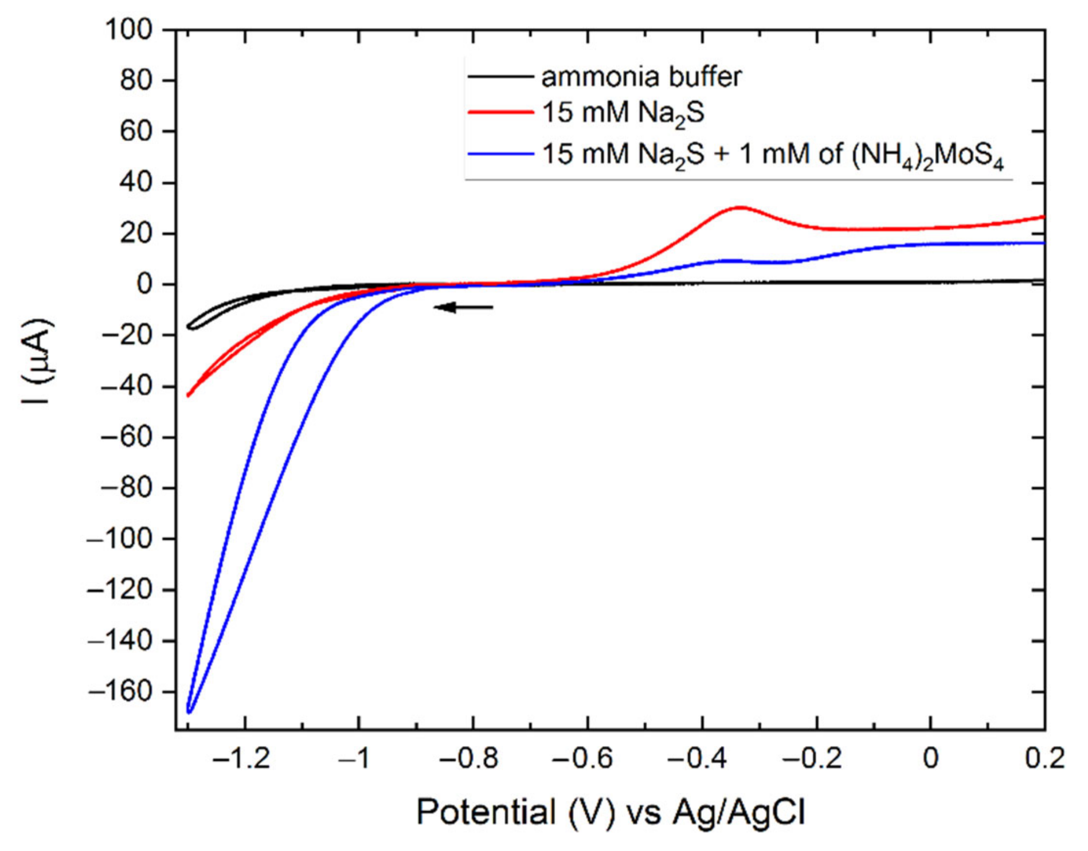
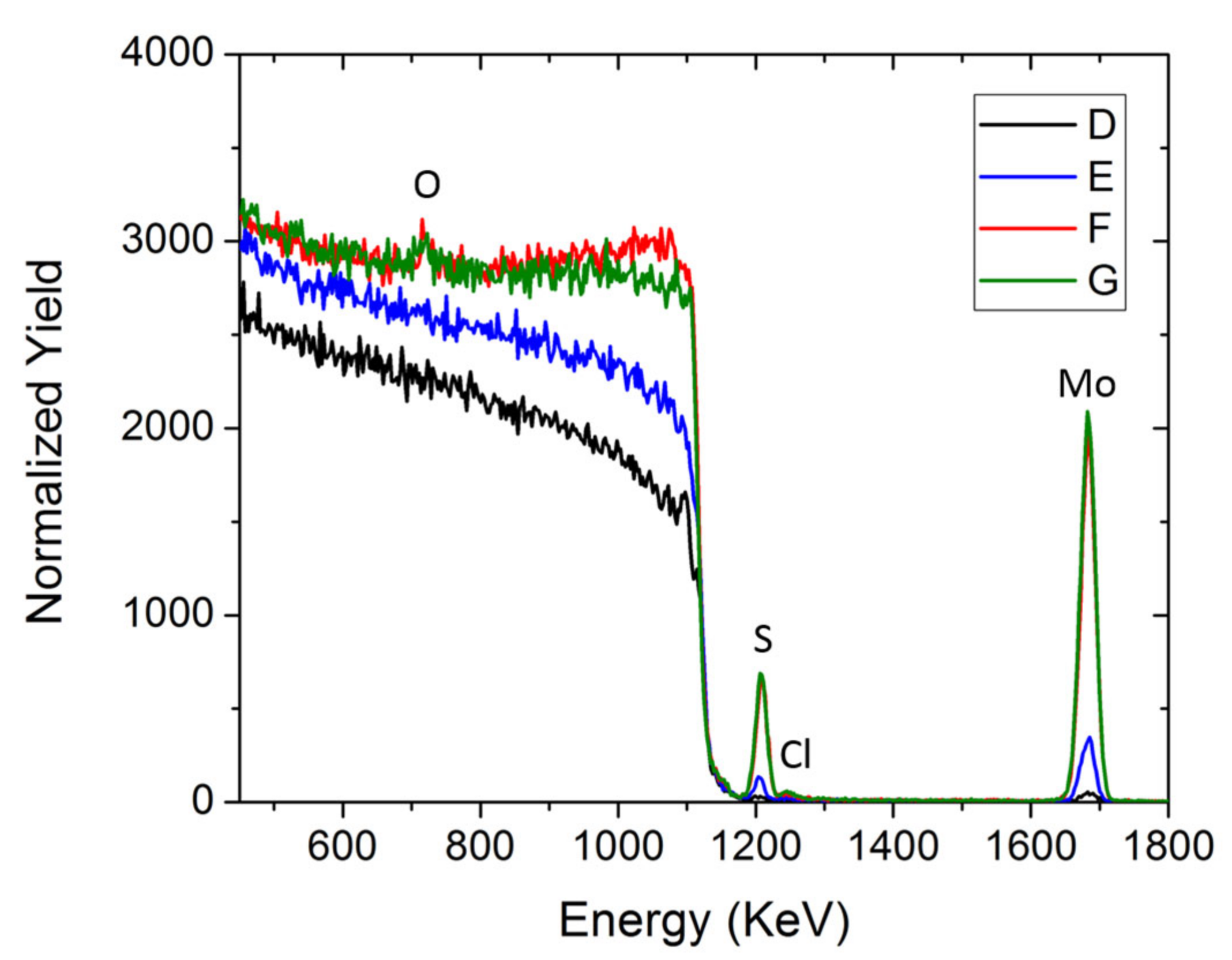
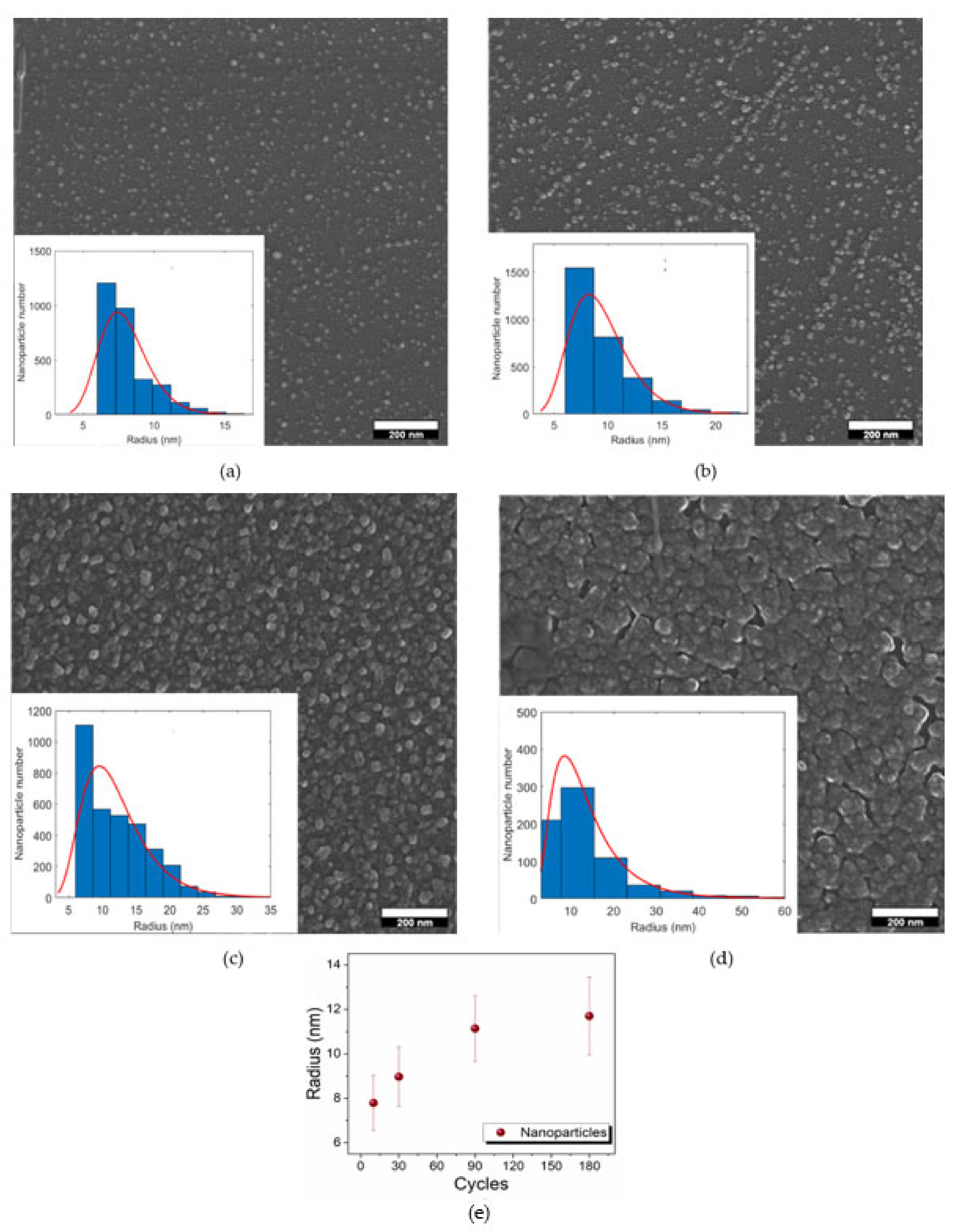
2. Results
3. Materials and Methods
3.1. Electrochemical Measurements
3.2. Microscopic and Spectroscopic Characterization
4. Conclusions
Author Contributions
Funding
Institutional Review Board Statement
Informed Consent Statement
Conflicts of Interest
Sample Availability
References
- Samy, O.; El Moutaouakil, A. A Review on Mos2 Energy Applications: Recent Developments and Challenges. Crystals 2021, 11, 355. [Google Scholar] [CrossRef]
- Alinejadian, N.; Kollo, L.; Odnevall, I. Progress in Additive Manufacturing of MoS2-Based Structures for Energy Storage Applications—A Review. Mater. Sci. Semicond. Process. 2022, 139, 106331. [Google Scholar] [CrossRef]
- Lv, Y.; Chen, P.; Foo, J.J.; Zhang, J.; Qian, W.; Chen, C.; Ong, W.J. Dimensionality-Dependent MoS2 toward Efficient Photocatalytic Hydrogen Evolution: From Synthesis to Modifications in Doping, Surface and Heterojunction Engineering. Mater. Today Nano 2022, 18, 100191. [Google Scholar] [CrossRef]
- Aliyev, A.S.; Elrouby, M.; Cafarova, S.F. Electrochemical Synthesis of Molybdenum Sulfide Semiconductor. Mater. Sci. Semicond. Process. 2015, 32, 31–39. [Google Scholar] [CrossRef]
- Radisavljevic, B.; Radenovic, A.; Brivio, J.; Giacometti, V.; Kis, A. Single-Layer MoS2 Transistors. Nat. Nanotechnol. 2011, 6, 147–150. [Google Scholar] [CrossRef] [PubMed]
- Theerthagiri, J.; Senthil, R.A.; Senthilkumar, B.; Reddy Polu, A.; Madhavan, J.; Ashokkumar, M. Recent Advances in MoS2 Nanostructured Materials for Energy and Environmental Applications-A Review. J. Solid State Chem. 2017, 252, 43–71. [Google Scholar] [CrossRef]
- Son, M.; Jang, J.; Kim, D.C.; Lee, S.; Shin, H.S.; Ham, M.H.; Chee, S.S. Fabrication of Large-Area Molybdenum Disulfide Device Arrays Using Graphene/Ti Contacts. Molecules 2021, 26, 4394. [Google Scholar] [CrossRef]
- Lan, Z.; Gao, S.; Wu, J.; Lin, J. High-Performing Dye-Sensitized Solar Cells Based on Reduced Graphene Oxide/PEDOT-PSS Counter Electrodes with Sulfuric Acid Post-Treatment. J. Appl. Polym. Sci. 2015, 132, 1–5. [Google Scholar] [CrossRef]
- Yin, X.; Wu, F.; Fu, N.; Han, J.; Chen, D.; Xu, P.; He, M.; Lin, Y. Facile Synthesis of Poly(3,4-Ethylenedioxythiophene) Film via Solid-State Polymerization as High-Performance Pt-Free Counter Electrodes for Plastic Dye-Sensitized Solar Cells. ACS Appl. Mater. Interfaces 2013, 5, 8423–8429. [Google Scholar] [CrossRef]
- Lopez-Sanchez, O.; Lembke, D.; Kayci, M.; Radenovic, A.; Kis, A. Ultrasensitive Photodetectors Based on Monolayer MoS 2. Nat. Nanotechnol. 2013, 8, 497–501. [Google Scholar] [CrossRef]
- Wang, Q.H.; Kalantar-Zadeh, K.; Kis, A.; Coleman, J.N.; Strano, M.S. Electronics and Optoelectronics of Two-Dimensional Transition Metal Dichalcogenides. Nat. Nanotechnol. 2012, 7, 699–712. [Google Scholar] [CrossRef]
- Wang, S.; Han, C.; Ye, L.; Zhang, G.; Hu, Y.; Li, W.; Jiang, Y. Electronic Properties of Triangle Molybdenum Disulfide (Mos2) Clusters with Different Sizes and Edges. Molecules 2021, 26, 1157. [Google Scholar] [CrossRef]
- Ratha, S.; Rout, C.S. Supercapacitor Electrodes Based on Layered Tungsten Disulfide-Reduced Graphene Oxide Hybrids Synthesized by a Facile Hydrothermal Method. ACS Appl. Mater. Interfaces 2013, 5, 11427–11433. [Google Scholar] [CrossRef]
- Hinnemann, B.; Moses, P.G.; Bonde, J.; Jørgensen, K.P.; Nielsen, J.H.; Horch, S.; Chorkendorff, I.; Nørskov, J.K. Biomimetic Hydrogen Evolution: MoS2 Nanoparticles as Catalyst for Hydrogen Evolution. J. Am. Chem. Soc. 2005, 127, 5308–5309. [Google Scholar] [CrossRef]
- Merki, D.; Hu, X. Recent Developments of Molybdenum and Tungsten Sulfides as Hydrogen Evolution Catalysts. Energy Environ. Sci. 2011, 4, 3878–3888. [Google Scholar] [CrossRef]
- Jing, Y.; Wang, R.; Wang, Q.; Wang, X. Gold Nanoclusters Grown on Mos2 Nanosheets by Pulsed Laser Deposition: An Enhanced Hydrogen Evolution Reaction. Molecules 2021, 26, 7503. [Google Scholar] [CrossRef]
- Kosmala, T.; Mosconi, D.; Giallongo, G.; Rizzi, G.A.; Granozzi, G. Highly Efficient MoS2/Ag2S/Ag Photoelectrocatalyst Obtained from a Recycled DVD Surface. ACS Sustain. Chem. Eng. 2018, 6, 7818–7825. [Google Scholar] [CrossRef]
- Quagraine, E.K.; Georgakaki, I.; Coucouvanis, D. Reactivity and Kinetic Studies of (NH4)2(MoS4) in Acidic Aqueous Solution: Possible Relevance to the Angiostatic Function of the MoS42− Ligand. J. Inorg. Biochem. 2009, 103, 143–155. [Google Scholar] [CrossRef]
- Yan, Y.; Xia, B.Y.; Zhao, B.; Wang, X. A Review on Noble-Metal-Free Bifunctional Heterogeneous Catalysts for Overall Electrochemical Water Splitting. J. Mater. Chem. A 2016, 4, 17587–17603. [Google Scholar] [CrossRef]
- Zhang, L.; Wu, L.; Li, J.; Lei, J. Electrodeposition of Amorphous Molybdenum Sulfide Thin Film for Electrochemical Hydrogen Evolution Reaction. BMC Chem. 2019, 13, 88. [Google Scholar] [CrossRef]
- Merki, D.; Vrubel, H.; Rovelli, L.; Fierro, S.; Hu, X. Fe, Co, and Ni Ions Promote the Catalytic Activity of Amorphous Molybdenum Sulfide Films for Hydrogen Evolution. Chem. Sci. 2012, 3, 2515–2525. [Google Scholar] [CrossRef]
- Levinas, R.; Tsyntsaru, N.; Cesiulis, H. The Characterisation of Electrodeposited MoS2 Thin Films on a Foam-Based Electrode for Hydrogen Evolution. Catalysts 2020, 10, 1182. [Google Scholar] [CrossRef]
- He, Z.; Que, W. Molybdenum Disulfide Nanomaterials: Structures, Properties, Synthesis and Recent Progress on Hydrogen Evolution Reaction. Appl. Mater. Today 2016, 3, 23–56. [Google Scholar] [CrossRef]
- Pan, Y.; Chen, S. Influence of Group Iii and Iv Elements on the Hydrogen Evolution Reaction of Mos2 Disulfide. J. Phys. Chem. C 2021, 125, 11848–11856. [Google Scholar] [CrossRef]
- Qu, J.; Li, Y.; Li, F.; Li, T.; Wang, X.; Yin, Y.; Ma, L.; Schmidt, O.G.; Zhu, F. Direct Thermal Enhancement of Hydrogen Evolution Reaction of On-Chip Monolayer MoS2. ACS Nano 2022, 16, 2921–2927. [Google Scholar] [CrossRef]
- Roy, K.; Maitra, S.; Ghosh, D.; Kumar, P.; Devi, P. 2D-Heterostructure Assisted Activation of MoS2 Basal Plane for Enhanced Photoelectrochemical Hydrogen Evolution Reaction. Chem. Eng. J. 2022, 435, 134963. [Google Scholar] [CrossRef]
- Wang, S.; Wang, L.; Xie, L.; Zhao, W.; Liu, X. Dislocation-Strained MoS2 Nanosheets for High-Efficiency Hydrogen Evolution Reaction. Nano Res. 2022, 2, 1–8. [Google Scholar] [CrossRef]
- Zou, X.; Zhang, Y. Noble Metal-Free Hydrogen Evolution Catalysts for Water Splitting. Chem. Soc. Rev. 2015, 44, 5148–5180. [Google Scholar] [CrossRef] [PubMed]
- Abdel Maksoud, M.I.A.; Bedir, A.G.; Bekhit, M.; Abouelela, M.M.; Fahim, R.A.; Awed, A.S.; Attia, S.Y.; Kassem, S.M.; Elkodous, M.A.; El-Sayyad, G.S.; et al. MoS2-Based Nanocomposites: Synthesis, Structure, and Applications in Water Remediation and Energy Storage: A Review; Springer International Publishing: Cham, Switzerland, 2021; Volume 19, ISBN 0123456789. [Google Scholar]
- Liu, C.; Kong, C.; Zhang, F.J.; Kai, C.M.; Cai, W.Q.; Sun, X.Y.; Oh, W.C. Research Progress of Defective MoS2 for Photocatalytic Hydrogen Evolution. J. Korean Ceram. Soc. 2021, 58, 135–147. [Google Scholar] [CrossRef]
- Yuan, Y.; Guo, R.T.; Hong, L.F.; Ji, X.Y.; Li, Z.W.; Lin, Z.D.; Pan, W.G. Recent Advances and Perspectives of MoS2-Based Materials for Photocatalytic Dyes Degradation: A Review. Colloids Surf. A Physicochem. Eng. Asp. 2021, 611, 125836. [Google Scholar] [CrossRef]
- Benck, J.D.; Hellstern, T.R.; Kibsgaard, J.; Chakthranont, P.; Jaramillo, T.F. Catalyzing the Hydrogen Evolution Reaction (HER) with Molybdenum Sulfide Nanomaterials. ACS Catal. 2014, 4, 3957–3971. [Google Scholar] [CrossRef]
- Zhang, K.; Fu, Y.; Hao, D.; Guo, J.; Ni, B.J.; Jiang, B.; Xu, L.; Wang, Q. Fabrication of CN75/NH2-MIL-53(Fe) p-n Heterojunction with Wide Spectral Response for Efficiently Photocatalytic Cr(VI) Reduction. J. Alloys Compd. 2022, 891, 161994. [Google Scholar] [CrossRef]
- Chen, S.; Pan, Y. Enhancing Catalytic Properties of Noble Metal@MoS2/WS2 Heterojunction for the Hydrogen Evolution Reaction. Appl. Surf. Sci. 2022, 591, 153168. [Google Scholar] [CrossRef]
- Fu, Y.; Zhang, K.; Zhang, Y.; Cong, Y.; Wang, Q. Fabrication of Visible-Light-Active MR/NH2-MIL-125(Ti) Homojunction with Boosted Photocatalytic Performance. Chem. Eng. J. 2021, 412, 128722. [Google Scholar] [CrossRef]
- Shah, S.A.; Khan, I.; Yuan, A. MoS2 as a Co-Catalyst for Photocatalytic Hydrogen Production: A Mini Review. Molecules 2022, 27, 3289. [Google Scholar] [CrossRef] [PubMed]
- Laursen, A.B.; Pedersen, T.; Malacrida, P.; Seger, B.; Hansen, O.; Vesborg, P.C.K.; Chorkendorff, I. MoS2-An Integrated Protective and Active Layer on n+p-Si for Solar H2 Evolution. Phys. Chem. Chem. Phys. 2013, 15, 20000–20004. [Google Scholar] [CrossRef] [PubMed]
- Leonardi, A.A.; Lo Faro, M.J.; Di Franco, C.; Palazzo, G.; D’Andrea, C.; Morganti, D.; Manoli, K.; Musumeci, P.; Fazio, B.; Lanza, M.; et al. Silicon Nanowire Luminescent Sensor for Cardiovascular Risk in Saliva. J. Mater. Sci. Mater. Electron. 2020, 31, 10–17. [Google Scholar] [CrossRef]
- Leonardi, A.A.; Faro, M.J.L.; Irrera, A. CMOS-Compatible and Low-Cost Thin Film MACE Approach for Light-Emitting Si NWs Fabrication. Nanomaterials 2020, 10, 966. [Google Scholar] [CrossRef]
- Lo Faro, M.J.; Leonardi, A.A.; Priolo, F.; Fazio, B.; Miritello, M.; Irrera, A. Erbium Emission in Er:Y2O3 Decorated Fractal Arrays of Silicon Nanowires. Sci. Rep. 2020, 10, 2854. [Google Scholar] [CrossRef]
- Gabrielli, L.H.; Cardenas, J.; Poitras, C.B.; Lipson, M. Silicon Nanostructure Cloak Operating at Optical Frequencies. Nat. Photonics 2009, 3, 461–463. [Google Scholar] [CrossRef] [Green Version]
- Zhou, K.G.; Mao, N.N.; Wang, H.X.; Peng, Y.; Zhang, H.L. A mixed-solvent strategy for efficient exfoliation of inorganic graphene analogues. Angewandte Chemie. 2011, 123, 11031–11034. [Google Scholar] [CrossRef]
- Irrera, A.; Lo Faro, M.J.; D’Andrea, C.; Alessio Leonardi, A.; Artoni, P.; Fazio, B.; Anna Picca, R.; Cioffi, N.; Trusso, S.; Franzo, G.; et al. Light-Emitting Silicon Nanowires Obtained by Metal-Assisted Chemical Etching. Semicond. Sci. Technol. 2017, 32, 043004. [Google Scholar] [CrossRef]
- Luo, Z.; Wang, T.; Gong, J. Single-Crystal Silicon-Based Electrodes for Unbiased Solar Water Splitting: Current Status and Prospects. Chem. Soc. Rev. 2019, 48, 2158–2181. [Google Scholar] [CrossRef]
- Sun, K.; Shen, S.; Liang, Y.; Burrows, P.E.; Mao, S.S.; Wang, D. Enabling Silicon for Solar-Fuel Production. Chem. Rev. 2014, 114, 8662–8719. [Google Scholar] [CrossRef]
- Peter, L.M.; Upul Wijayantha, K.G. Photoelectrochemical Water Splitting at Semiconductor Electrodes: Fundamental Problems and New Perspectives. ChemPhysChem 2014, 15, 1983–1995. [Google Scholar] [CrossRef]
- Benck, J.D.; Chen, Z.; Kuritzky, L.Y.; Forman, A.J.; Jaramillo, T.F. Amorphous Molybdenum Sulfide Catalysts for Electrochemical Hydrogen Production: Insights into the Origin of Their Catalytic Activity. ACS Catal. 2012, 2, 1916–1923. [Google Scholar] [CrossRef]
- Cai, W.; Xiong, H.; Su, X.; Zhou, H.; Shen, M.; Fang, L. Enhanced Photoelectrochemical Properties of Copper-Assisted Catalyzed Etching Black Silicon by Electrodepositing Cobalt. Appl. Phys. Lett. 2017, 111, 203902. [Google Scholar] [CrossRef]
- Radisavljevic, B.; Whitwick, M.B.; Kis, A. Integrated Circuits and Logic Operations Based on Single-Layer MoS 2. ACS Nano 2011, 5, 9934–9938. [Google Scholar] [CrossRef]
- Rao, C.N.R.; Nag, A. Inorganic Analogues of Graphene. Eur. J. Inorg. Chem. 2010, 2010, 4244–4250. [Google Scholar] [CrossRef]
- Huo, J.; Ge, R.; Liu, Y.; Guo, J.; Lu, L.; Chen, W.; Liu, C.; Gao, H.; Liu, H. Recent Advances of Two–Dimensional Molybdenum Disulfide Based Materials: Synthesis, Modification and Applications in Energy Conversion and Storage. Sustain. Mater. Technol. 2020, 24, e00161. [Google Scholar] [CrossRef]
- Park, H.; Liu, N.; Kim, B.H.; Kwon, S.H.; Baek, S.; Kim, S.; Lee, H.K.; Yoon, Y.J.; Kim, S. Exceptionally Uniform and Scalable Multilayer MoS2 Phototransistor Array Based on Large-Scale MoS2 Grown by RF Sputtering, Electron Beam Irradiation, and Sulfurization. ACS Appl. Mater. Interfaces 2020, 12, 20645–20652. [Google Scholar] [CrossRef]
- Lauritsen, J.V.; Kibsgaard, J.; Helveg, S.; Topsøe, H.; Clausen, B.S.; Lægsgaard, E.; Besenbacher, F. Size-Dependent Structure of MoS 2 Nanocrystals. Nat. Nanotechnol. 2007, 2, 53–58. [Google Scholar] [CrossRef]
- Seravalli, L.; Bosi, M. A Review on Chemical Vapour Deposition of Two-Dimensional MoS2 Flakes. Materials 2021, 14, 7590. [Google Scholar] [CrossRef]
- Schilirò, E.; Lo Nigro, R.; Roccaforte, F.; Giannazzo, F. Substrate-Driven Atomic Layer Deposition of High-κ Dielectrics on 2d Materials. Appl. Sci. 2021, 11, 11052. [Google Scholar] [CrossRef]
- Giurlani, W.; Vizza, M.; Leonardi, A.A.; Lo Faro, M.J.; Irrera, A.; Innocenti, M. Optimization and Characterization of Electrodeposited Cadmium Selenide on Monocrystalline Silicon. Nanomaterials 2022, 12, 610. [Google Scholar] [CrossRef]
- Gurulakshmi, M.; Meenakshamma, A.; Siddeswaramma, G.; Susmitha, K.; Venkata Subbaiah, Y.P.; Narayana, T.; Raghavender, M. Electrodeposited MoS2 Counter Electrode for Flexible Dye Sensitized Solar Cell Module with Ionic Liquid Assisted Photoelectrode. Sol. Energy 2020, 199, 447–452. [Google Scholar] [CrossRef]
- Hossain, M.A.; Merzougui, B.A.; Alharbi, F.H.; Tabet, N. Electrochemical Deposition of Bulk MoS2 Thin Films for Photovoltaic Applications. Sol. Energy Mater. Sol. Cells 2018, 186, 165–174. [Google Scholar] [CrossRef]
- Levinas, R.; Tsyntsaru, N.; Cesiulis, H. Insights into Electrodeposition and Catalytic Activity of MoS2 for Hydrogen Evolution Reaction Electrocatalysis. Electrochim. Acta 2019, 317, 427–436. [Google Scholar] [CrossRef]
- Ponomarev, E.A.; Neumann-Spallart, M.; Hodes, G.; Lévy-Clément, C. Electrochemical Deposition of MoS2 Thin Films by Reduction of Tetrathiomolybdate. Thin Solid Films 1996, 280, 86–89. [Google Scholar] [CrossRef]
- Wang, X.; Cormier, C.R.; Khosravi, A.; Smyth, C.M.; Shallenberger, J.R.; Addou, R.; Wallace, R.M. In Situ Exfoliated 2D Molybdenum Disulfide Analyzed by XPS. Surf. Sci. Spectra 2020, 27, 014019. [Google Scholar] [CrossRef]
- Forni, F.; Innocenti, M.; Pezzatini, G.; Foresti, M. Electrochemical Aspects of CdTe Growth on the Face (111) of Silver by ECALE. Electrochim. Acta 2000, 45, 3225–3231. [Google Scholar] [CrossRef]
- Shirley, D.A. High-Resolution X-ray Photoemission Spectrum of the Valence Bands of Gold. Phys. Rev. B 1972, 5, 4709–4714. [Google Scholar] [CrossRef]
- Susi, T.; Pichler, T.; Ayala, P. X-ray Photoelectron Spectroscopy of Graphitic Carbon Nanomaterials Doped with Heteroatoms. Beilstein J. Nanotechnol. 2015, 6, 177–192. [Google Scholar] [CrossRef] [Green Version]


| Sample | Deposition Potential | Total Deposited Charge | Number of Cycles | Deposited Charge/Cycle |
|---|---|---|---|---|
| A | –1.0 V | 6 mC | 30 | 200 µC |
| B | –1.1 V | 6 mC | 30 | 200 µC |
| C | –1.3 V | 6 mC | 30 | 200 µC |
| Sample | Deposition Potential | Total Deposited Charge | Number of Cycles | Deposited Charge/Cycle |
|---|---|---|---|---|
| D | –1.1 V | 2 mC | 10 | 200 µC |
| E | –1.1 V | 6 mC | 30 | 200 µC |
| F | –1.1 V | 18 mC | 90 | 200 µC |
| G | –1.1 V | 36 mC | 180 | 200 µC |
| Sample | S 10 15 at/cm2 | Mo 10 15 at/cm2 | O 10 15 at/cm2 | S/Mo |
|---|---|---|---|---|
| D | 2.14 ± 0.06 | 0.85 ± 0.03 | -- | 2.52 ± 0.15 |
| E | 8.80 ± 0.26 | 4.48 ± 0.13 | -- | 1.96 ± 0.12 |
| F | 39.90 ± 1.20 | 23.1 ± 0.69 | 32.55 ± 0.98 | 1.73 ± 0.10 |
| G | 47.62 ± 1.43 | 25.17 ± 0.75 | 40.04 ± 1.20 | 1.89 ± 0.11 |
Publisher’s Note: MDPI stays neutral with regard to jurisdictional claims in published maps and institutional affiliations. |
© 2022 by the authors. Licensee MDPI, Basel, Switzerland. This article is an open access article distributed under the terms and conditions of the Creative Commons Attribution (CC BY) license (https://creativecommons.org/licenses/by/4.0/).
Share and Cite
Vizza, M.; Giurlani, W.; Cerri, L.; Calisi, N.; Leonardi, A.A.; Faro, M.J.L.; Irrera, A.; Berretti, E.; Perales-Rondón, J.V.; Colina, A.; et al. Electrodeposition of Molybdenum Disulfide (MoS2) Nanoparticles on Monocrystalline Silicon. Molecules 2022, 27, 5416. https://doi.org/10.3390/molecules27175416
Vizza M, Giurlani W, Cerri L, Calisi N, Leonardi AA, Faro MJL, Irrera A, Berretti E, Perales-Rondón JV, Colina A, et al. Electrodeposition of Molybdenum Disulfide (MoS2) Nanoparticles on Monocrystalline Silicon. Molecules. 2022; 27(17):5416. https://doi.org/10.3390/molecules27175416
Chicago/Turabian StyleVizza, Martina, Walter Giurlani, Lorenzo Cerri, Nicola Calisi, Antonio Alessio Leonardi, Maria Josè Lo Faro, Alessia Irrera, Enrico Berretti, Juan Víctor Perales-Rondón, Alvaro Colina, and et al. 2022. "Electrodeposition of Molybdenum Disulfide (MoS2) Nanoparticles on Monocrystalline Silicon" Molecules 27, no. 17: 5416. https://doi.org/10.3390/molecules27175416
APA StyleVizza, M., Giurlani, W., Cerri, L., Calisi, N., Leonardi, A. A., Faro, M. J. L., Irrera, A., Berretti, E., Perales-Rondón, J. V., Colina, A., Bujedo Saiz, E., & Innocenti, M. (2022). Electrodeposition of Molybdenum Disulfide (MoS2) Nanoparticles on Monocrystalline Silicon. Molecules, 27(17), 5416. https://doi.org/10.3390/molecules27175416