1. Introduction
Zinc oxide has been applied in many fields; including gas sensors, photodiodes, lithium-ion batteries and particularly solar cells. ZnO can be easily fabricated into various morphologies (e.g., nanowires, nanorods, nanotubes, nanoflowers, nanosheets) on different substrates. Therefore, ZnO in different shapes and in composites is studied for various applications. Recently, some authors combined ZnO in heterostructure with CdS [
1,
2] and studied its photocatalytic properties. ZnO in the form of thin film with CdS nanoparticles on the surface has been shown to be a high-performance material for photocatalytic degradation of methylene blue [
1], while ZnO/CdS hierarchical composites have shown great photocatalytic H
2-production performance [
2]. Wu et al. [
3] prepared ZnO hollow spheres and the hedgehog-like ZnO hollow spheres and studied their use as anodes for lithium-ion batteries, having good rate capacity, cycling performance, and high initial specific capacity. ZnO nanowires have prominent electron transport properties [
4], which are beneficial for solar cell application. However, ZnO is not chemically stable and is prone to dissolution. One way to avoid this fact is to coat a chemically stable shell on ZnO nanowires [
5].
On the other hand, nanostructured titanium dioxide is known as a material with notable physical and chemical properties, such as high photo-activity and environmental stability, as well as low cost synthesis. TiO
2 exists in nature in three different crystalline phases: anatase, rutile, and brookite, but it was found that anatase (band gap ~3.2 eV) is more photo-active than other modifications. It is widely used for photovoltaic applications [
6], primarily as an electron transport layer (ETL) in perovskite and dye sensitized solar cells, due to a suitable band gap for the acceptance of electrons from the active layer of solar cells. The studies aimed to improve the optical and transport properties of TiO
2-based electron conduction layers, which are of considerable importance for the enhancement of photovoltaic performance. By a combination of the high reactivity of TiO
2 and the large binding energy of ZnO, the process of electron transfer between the corresponding conduction and valence bands can be facilitated in the composite system [
7].
In comparison to mesoporous thin films on transparent conductive oxide (TCO) operated as ETL in solar cells, 1-dimensional (1D) nanostructures on TCO substrates can provide a direct pathway for electron transport and offer open channels for filling with light absorbers and HTMs for solar cells. Moreover, oriented nanorod-like materials on TCO are known for their efficient charge separation and transport properties and are thus favorable for achieving good device performance [
8,
9,
10]. Therefore, growth of oriented nanorods (NRs) on TCO substrates has drawn extensive research interest in solar energy utilization in the past years.
Moreover, the utilization of the single-crystalline 1D nanostructures with preferred orientation for ETL decreases the number of grain boundaries that decrease conductivity, as was observed in studies on ZnO nanostructure [
11,
12,
13]. Thus, Wu et al. [
11] investigated rapidly synthesized ZnO nanowires for photodetector application and produced nanowires which consist of nanoparticles. They concluded that these nanowires have adsorption sites on the inter-granular surface, which can lead to the increased reactivity of these surfaces and, therefore, a low conductivity. Their finding is in accordance with old paper of Oktik [
12] where he stated that a large density of extrinsic electron traps, present at the grain boundaries due to oxygen chemisorption, results in a barrier to charge-carrier conduction at grain boundaries. Annealing in vacuum or in reducing atmosphere desorbs the oxygen and therefore decreases the grain boundary potential barrier and increases the effective charge-carrier concentration (and therefore the conductivity). Natsume and Sakata [
13] prepared ZnO films by sol–gel spin-coating and confirmed the grain boundary scattering effect due to thermionic emission.
Several groups prepared ZnO nanowires combined with other materials (polycrystalline MgO, P3HT polymer) in core–shell hetero-structures and studied their application in polymer and dye sensitized solar cells (DSSCs) [
14]. These hetero-structures combine stable characteristics from the shell and fast electron transport features of the mono-crystalline nanowire core, thus increasing the efficiency of solar cells. Samad et al. [
15] found that an enhancement of photocurrent density and photo conversion efficiency occurred due to the sufficient Ti content within TiO
2–ZnO nanorod films. This film traps the photo-induced electrons and minimizes the recombination of charge carriers, while the charge-separation effect at the type-II band alignment of Zn and Ti further enhances the charge carrier transport during illumination. Boroa et al. [
16] reviewed different TiO
2/ZnO nanocomposites for use as a photo-anode in DSSCs. They compared typical solar cells parameters (open circuit voltage, short circuit current, fill factor and efficiency) for nanocomposites such as TiO
2 doped or decorated with different sized ZnO nanostructures and vice versa, coaxial nanotube arrays, nanodonuts, nanoflowers and 3D hierarchical hetero-structures. It is concluded that the best performance among studied nanostructures was shown in DSSCs with one-dimensional composite structures such as nanotubes, nanorods, or nanowires. Recently, Zhong et al. [
17] synthesized ZnO nanorod arrays by polymer template and sol–gel methods for TiO
2 modification, starting from butyl titanate and isopropanol. They studied the use of such core–shell structures as ETL in perovskite solar cells (PSCs) and showed improved power conversion efficiency compared to pure ZnO nanorod arrays used as ETL. Enhanced stability in air was also observed. The same authors [
18] also studied the influence of the ZnO–TiO
2 nanorod length, prepared by the same procedure on PSCs efficiency and stability. All the cited results for photovoltaics with ZnO–TiO
2 composites as ETL indicated that the study of the influence of the TiO
2 deposition parameters on structure, morphology, and, consequently, on optical and electrical properties are of the main importance for further development of different photovoltaic devices. Therefore, detailed study of different preparation methods and the influence of the preparation parameters of the TiO
2 shell in ZnO@TiO
2 core–shell nanostructures would improve photovoltaic devices based on ZnO@TiO
2 core shell nanorod arrays as ETL.
ZnO with TiO
2 at the surface of the nanostructures are also used for other applications. Hernandez et al. [
19] have demonstrated that ZnO–TiO
2 materials have a superior photo-electrochemical activity, due to improved electron-hole separation and lower charge carrier recombination rates. They demonstrated a sol–gel synthesis for the deposition of a protective shell of anatase TiO
2 nanoparticles onto a vertically aligned ZnO nanowire (NW) array. It is reported that the presence of the TiO
2 shell in the core–shell nanostructure improves the charge separation efficiency, thanks to a potential barrier at the semiconductor/electrolyte interface, which limits the charge recombination. Therefore, in ZnO@TiO
2 core–shell nanostructures, the high electron mobility is coupled with the efficient separation of charge carriers between the TiO
2 shell and the ZnO core. Further, X. Yan et al. [
20] applied the heterogeneous nanostructure as an efficient way to improve light absorption and extend the carrier life time characteristics of the photocatalysts to extend the catalyst’s optical absorption range in a Zn/TiO
2 core-brush structure.
In this work, we focused on influence of the type of preparation technique and deposition parameters on the structure and morphology of ZnO@TiO2 core–shell hetero-structures and their correlation with optical and electrical properties. The aim was to achieve a simple and low-cost preparation process of ZnO@TiO2 core–shell nanostructures and to understand their electrical and optical properties intended for photovoltaic application. However, the essential goal was to preserve transparency and to obtain superior electron transport properties of the formed ZnO@TiO2 core–shell nanorod array layers, so different deposition techniques for preparation of theTiO2 layers were studied. The ZnO nanorod arrays were prepared by a simple chemical method, while for TiO2 deposition on the ZnO nanorods, three different methods were studied—pulsed laser deposition (PLD), magnetron sputtering (MS), and spin coating of a chemically prepared precursor for the TiO2 layer, followed by annealing. The morphology and crystal structure of the deposited TiO2 is considerably dependent on the deposition method. The preparation parameters were chosen to obtain an anatase structure of the TiO2 shell. A significant absorption in the UV part of the spectrum was observed for all the prepared morphologies, while the absorption of visible light depends on the morphology of the TiO2 layer. The superior electrical properties in comparison to uncovered ZnO nanorods and bare TiO2 layers were observed in the thin layer of ZnO@TiO2 core–shell nanostructures. Thus, high surface conductivity for electrons as charge carriers as well as low activation energy was observed for all the core–shell nanostructures. The best electrical and optical properties among the studied samples were obtained for core–shell nanostructures where the TiO2 layer was prepared by chemical deposition, which was explained by homogenous coverage of the ZnO nanorods as well as by the smoothness of the TiO2 surface.
3. Discussion
Since it is known from literature [
6,
7,
14,
15,
16,
17,
18] that ZnO@TiO
2 core–shell nanostructures could serve as an advantageous electron transport layer in perovskite, polymer, and dye sensitized solar cells, influence of the morphology and structure on electrical and optical properties, that are crucial for photovoltaic application, were studied. To obtain ZnO@TiO
2 core–shell nanostructures with diverse structural properties, different deposition techniques were applied for the preparation of the shell layer, and the deposition parameters were additionally varied. In contrast to known literature where usually one chemical method was applied for the preparation of the TiO
2 shell layer on ZnO, in this study the focus was on the influence of different preparation methods (two physical and one chemical) on properties of the core–shell structure. Depending on the deposition techniques, we obtained 3 different morphologies of TiO
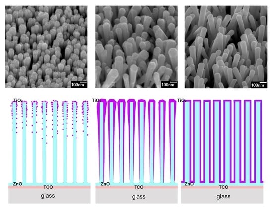
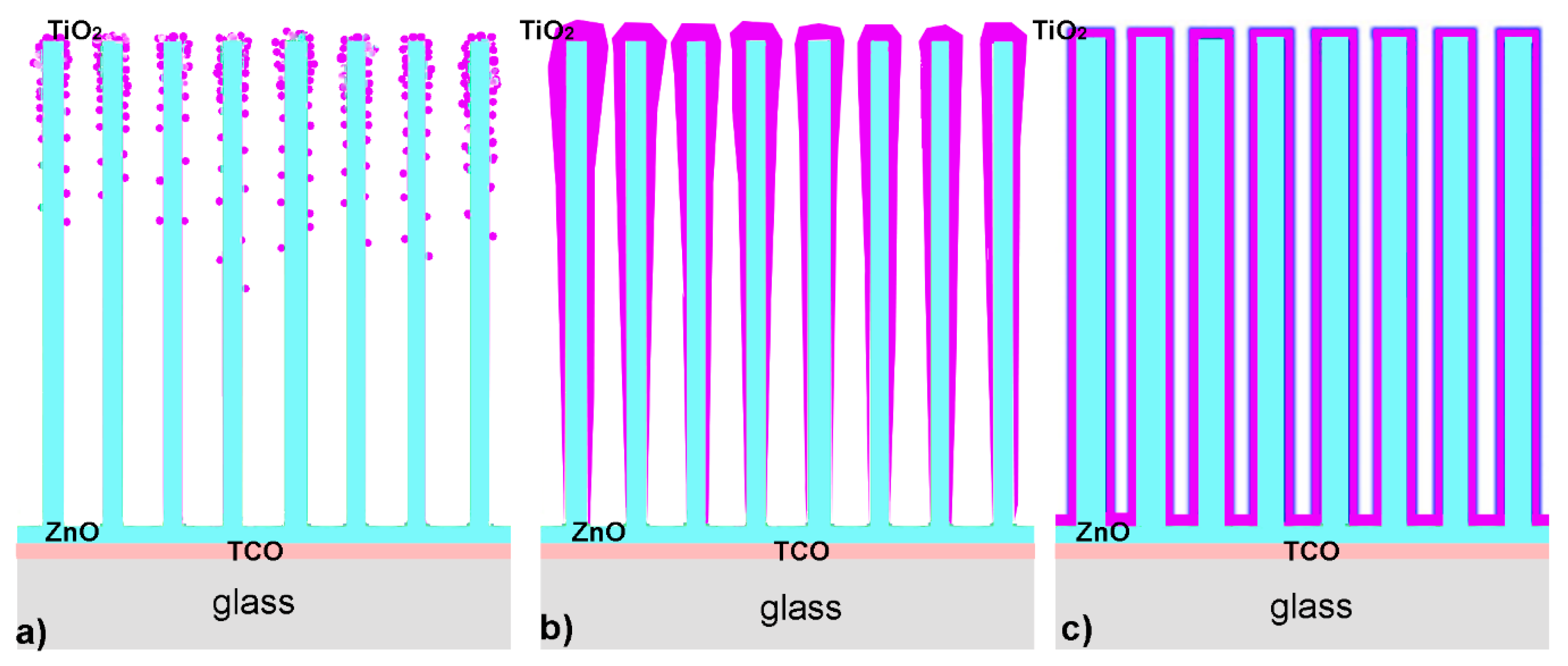
2 shell layers (
Figure 7). As was expected, the morphology of the shell layer affected the electrical and optical properties responsible for future application in photovoltaics. The main morphologies of TiO
2 layers: (1) nanoparticles or nanoaggregates on the surface of nanorods schematically represented by
Figure 7a, (2) a layer that preferably covers the upper part of nanorods, thicker at the top of nanorods, represented by
Figure 7b, and (3) a layer of TiO
2 that is homogenously distributed along the whole length of nanorods, represented by
Figure 7c. The first morphology was observed for ZnO@TiO
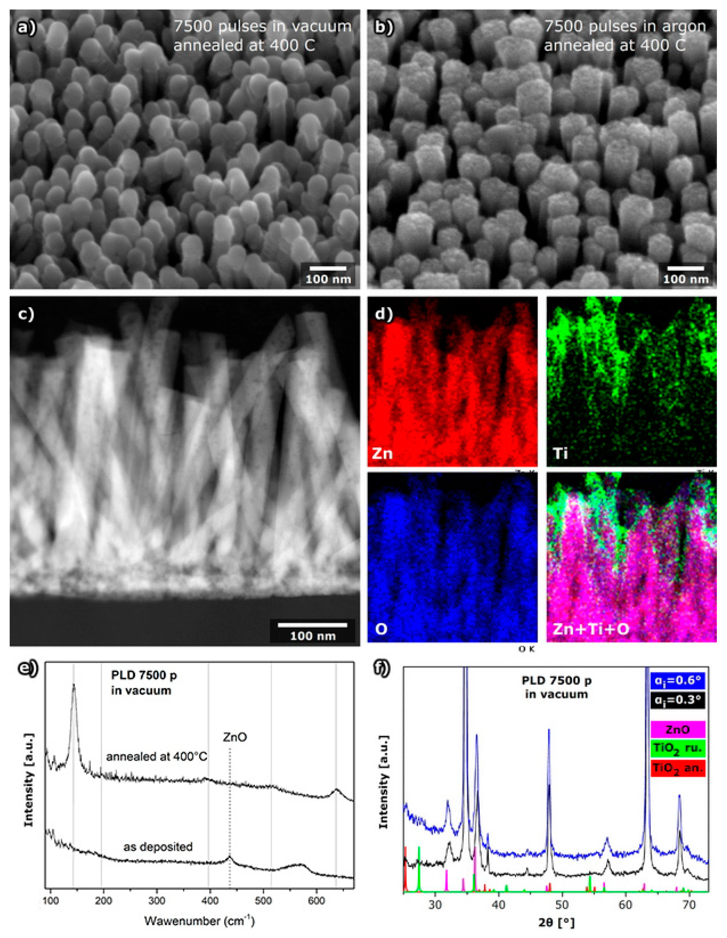
2 core shell nanorods obtained by PLD in argon. The second morphology was characteristic for TiO
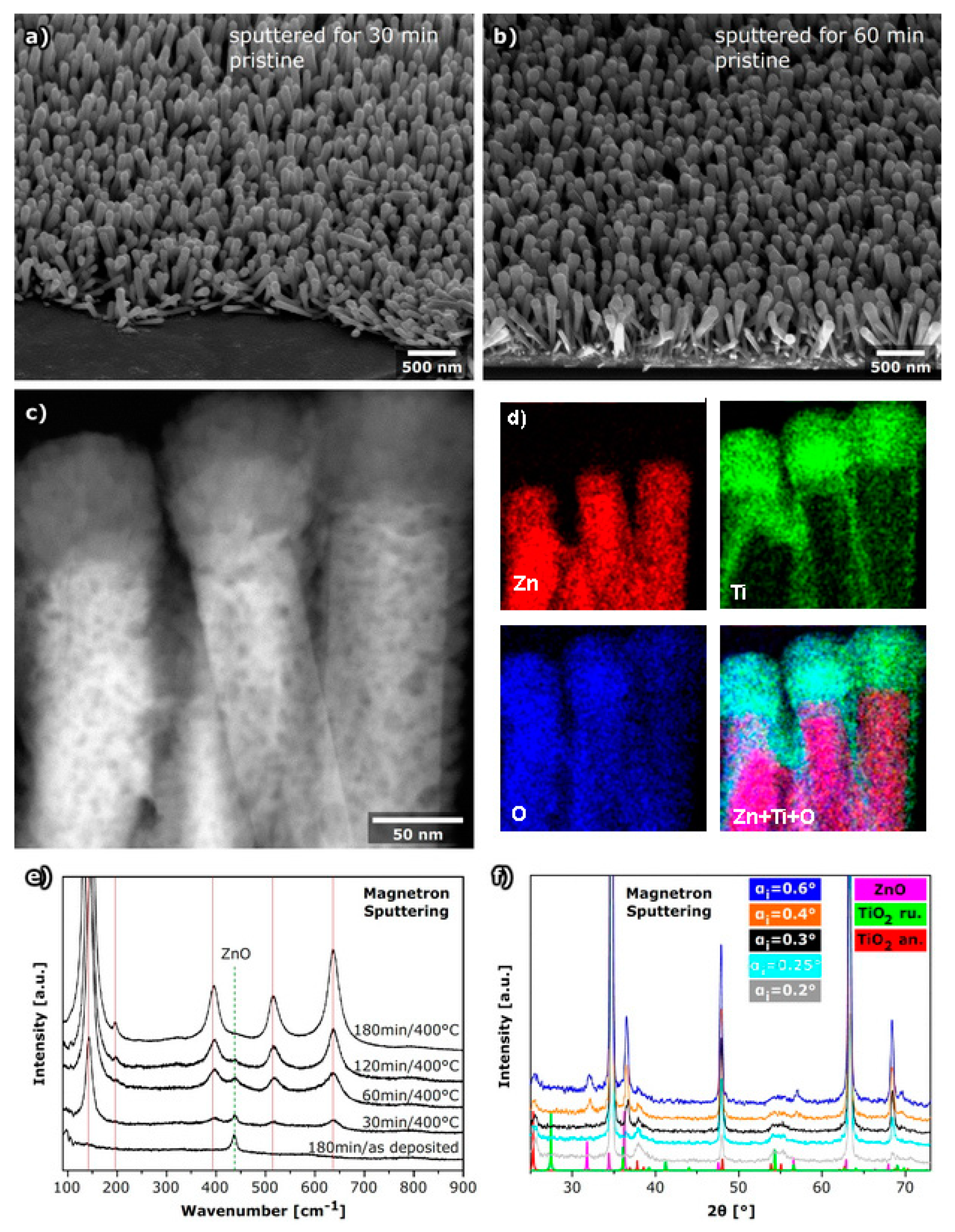
2 layers deposited by PLD in a vacuum or by magnetron sputtering, while the homogenously covered nanorods were prepared by chemical deposition.
The preparation parameters of each method influenced the thickness of the TiO
2 layer. Thicker layers were obtained by more laser pulses for PLD deposition, for longer time of MS deposition, or by more layers applied by spin coating. For the larger thickness of TiO
2 layers prepared by MS or chemical deposition, the nanorods were completely cluttered with TiO
2 (
Figure S3 and
Figure 4b). Since for thicker layers the optical properties are poor due to lower transparency, the optical and electrical properties were studied only for the samples with thinner TiO
2 layers.
The structural study indicated that as deposited layers were amorphous, so all the layers were additionally annealed after deposition to obtain crystallinity. Since anatase TiO2 has better optical properties, the heating temperature was chosen to obtain a pure anatase structure of the shell layer. It was observed that a relatively low heating temperature of only 400 °C should be applied to obtain an anatase structure of the TiO2 shell layer, since at 450 °C the partial phase transition to rutile was already observed, although the phase transition to rutile is around 1000 °C for large monocrystals of TiO2. The low temperature of phase transition was explained by small particles/clusters or very thin layers of amorphous TiO2 that accelerate the phase transition even at so low a temperature as 400 °C.
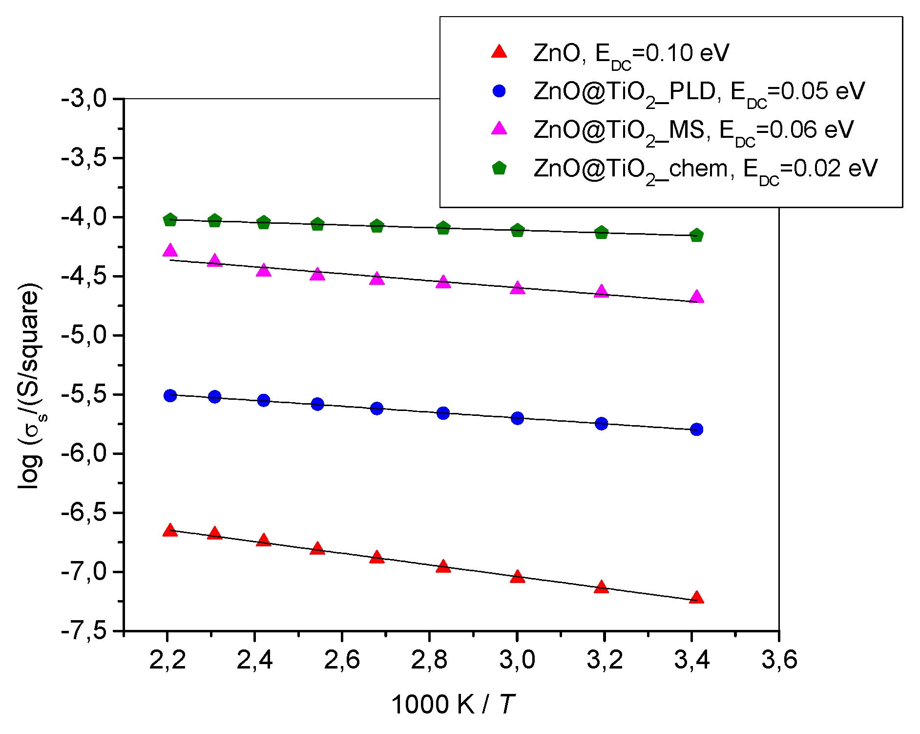
The impedance spectroscopy measurements show pure electron conductivity that was considerably larger in formed nanostructures than in the bare ZnO nanorod array or bare TiO2 layer. The highest conductivity and the lowest activation energy among the studied samples were observed for the sample with a chemically deposited TiO2 shell. This result can be explained by the homogenousTiO2 layer at the nanorod surface. The homogeneity was achieved, as during chemical deposition the precursor in the form of solution was spin coated at the surface of ZnO NR and can penetrate between nanorods, so that after heating, the formed TiO2 was distributed along the nanorods.
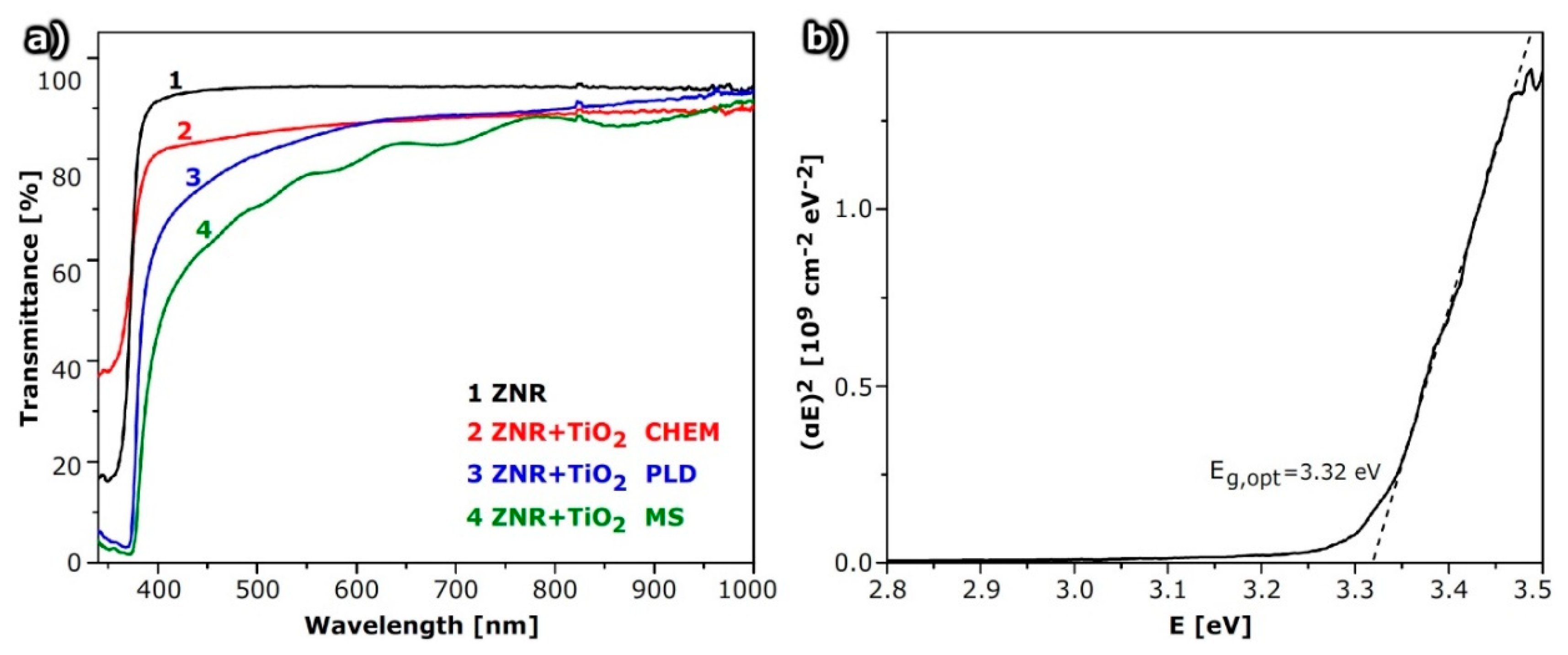
Optical measurements show the absorption in the UV part of the spectrum for all the morphologies, but the absorption in the visible part depends on the morphology of the TiO2 layer. The highest transparency among the studied samples was achieved for samples formed by chemical deposition, which can be explained both by the thickness of the layer as well as the homogeneity.
In comparison with data obtained for similar nanostructures presented in literature [
32], our samples showed higher transmission and better conductivity. Ahmadi et al. [
32] prepared ZnO/TiO
2 composite core–shell nanorod arrays by sol–gel process and dip coating, and measured transmittance that was lower than 60% in the visible part of the spectrum and even lower than 40% in the spectral region under 450 nm; while in our study, we obtained more than 80% transmittance. Resistivity of our core–shell structures varied between 10
4 and 10
6 Ω (
Figure 5). This value corresponds to the specific resistivity in the range between 1 and 10 Ωcm, which is much lower than in [
32]. On the other hand, if we compare our results of optical measurements obtained for arrays of 1-dimensional ZnO@TiO
2 core–shell nanorod arrays with results obtained from compact TiO
2/ZnO composite thin films studied by Giannakopoulou et al. [
33], it can be seen that our transmittance in the visible part of the solar spectrum is comparable to or slightly lower than that obtained from compact TiO
2/ZnO thin films [
33]. However, their thin films are considerably thinner (thicknesses are approximately 60–145 nm) in comparison to height of our ZnO@TiO
2 core–shell nanorods that form arrays (>300 nm), thus indicating the much better optical properties of our core–shell nanorod arrays.
We can compare the optical properties of the obtained ZnO@TiO
2 core–shell nanorods studied in this work with the optical properties obtained by Zou et al. [
34] for ZnO/V
2O
5 composite core–shell nanorod arrays with similar morphologies as our samples. It could be seen that for their as-prepared samples, the absorption edge is shifted to a larger wavelength, even to around 500 nm, while for samples annealed at 500 °C, considerable absorption of the light was observed in the completely visible region. Therefore, they have suggested the use of these nanocomposites for photocatalytic applications with visible light or natural sunlight [
34].
The prominent electron transport and optical properties of our ZnO@TiO2 core–shell nanorod arrays seems promising for application as an electron transport layer in perovskite and dye-sensitized solar cells. Since we have found appropriate preparation parameters of the studied deposition methods to obtain preferable electrical and optical properties for photovoltaic applications, our next step will be the assembling of photovoltaics using the studied ZnO@TiO2 core–shell nanorod arrays and a study of their performance in correlation with the TiO2 shell layer preparation method types and parameters.
4. Materials and Methods
The following materials and chemicals were used: ITO glass slides (20 × 15 mm, Ossila), Ti and TiO2 targets (for magnetron and pulsed laser depositions), deionized water (Milipore), acetone, ethanol (EtOH, aps.), zinc acetate dihydrate (ZA), zinc nitrate hexahydrate (ZN), hexamethylentetramine (HMT), titanium isopropoxide (TiPr), ethylene glycol monomethyl ether (EGME), monoethanolamine (MEA). All of the materials were analytical grade and used as received without further purification.
ZnO nanorods (ZNRs) were prepared in two steps. The first step was deposition of a ZnO seed layer by spin coating a solution of 0.25 M ZA in EtOH and MEA on previously cleaned (acetone, ethanol, and water in ultrasound for 10 min each, followed by UV ozone cleaner for 30 min) ITO substrates. After the deposition of the seed layer, the substrates were immersed in an aqueous solution of 0.125 M zinc nitrate hexahydrate and 0.125 M hexamethylenetetramine at 92 °C for 3 h. For electrical measurement, the ZnO seed layer and nanorods were grown directly on a glass (or quartz) surface to avoid artefacts in the conductivity measurement due to short circuits possibly caused by the mounting of contact electrodes.
ZNRs were further covered with TiO2 using two different physical deposition procedures and one chemical procedure. The evaluated procedures were: pulsed laser deposition (PLD), DC reactive magnetron sputtering, and spin coating of a chemically prepared precursor followed by annealing.
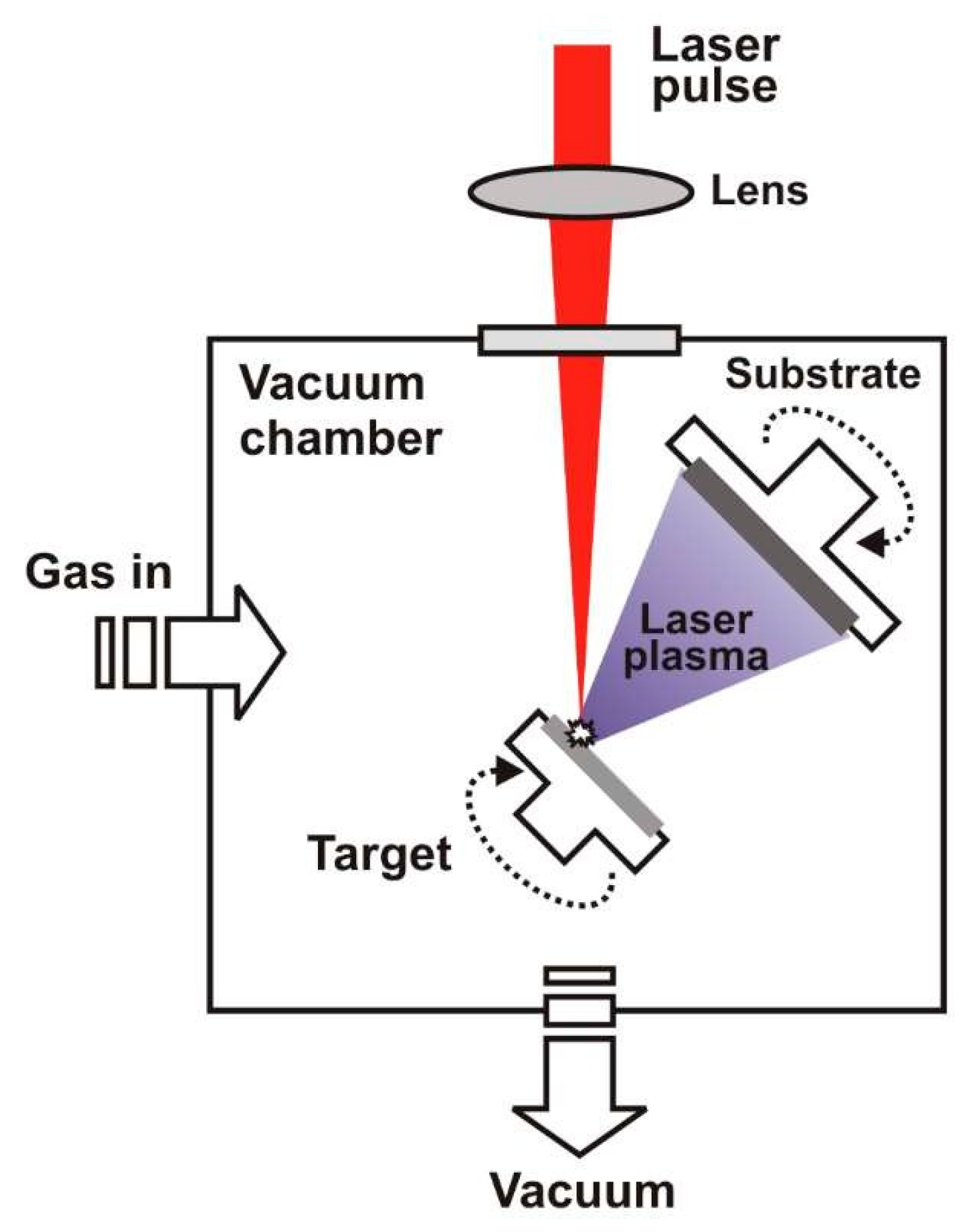
Pulsed laser deposition of TiO
2 thin films on the surface of ZNRs was done by using a Nd:YAG laser. The experimental setup is shown in
Figure 8. Laser parameters were: wavelength 1064 nm, pulse duration 4 ns, repetition rate 5 Hz, and output energy 340 mJ. Laser pulse energy in front of target was 150 mJ while laser pulses were focused on the target surface which yields a fluence of 20 J/cm
2. The distance between the target and substrate was 4 cm. The target surface was parallel to the substrate and inclined by 45° with respect to the impinging laser pulses. Both the target holder and the substrate were kept on floating potential and at room temperature during deposition and were rotated to avoid the drilling of the target and to increase the homogeneity of the deposited films. Films were deposited using 5000 and 7500 laser pulses. Deposition was performed either in a vacuum (pressure < 10
−3 mbar) or in 30 Pa of argon. After deposition, annealing at high temperature should be done to obtain crystallinity. The temperature of annealing was varied to obtain a pure anatase structure of TiO
2 and to avoid crystallization of the rutile TiO
2, so the temperatures of 400, 450, and 500 °C were applied.
Preparation of TiO
2 thin films on ZNRs by DC reactive magnetron sputtering was done using a 2″ Ti 99.999% target, an Ar + O
2 mixture as working gas and deposition parameters as listed in
Table 2. Depositions were done at room temperature. However, because of the interaction with plasma, substrate temperature was increased during the deposition to 60 °C. To obtain crystalline anatase, TiO
2 annealing was applied at temperatures between 400 and 500 °C.
The chemical deposition of TiO2 thin films on ZnO NRs was done by spin coating (4000 rpm, 30 s) the sol–gel solution of 0.125 M TiO2 (TiPr in EGME, MEA, and EtOH) and annealing at 400 or 450 °C after deposition.
The morphology of the samples was studied by scanning electron microscopy with a field emission gun (FEG-SEM) using JEOL JSM-700F (JEOL, Tokyo, Japan). The crystal structure on nanoscale was studied by transmission electron microscopy (TEM) using a JEOL-ARM300 microscope (JEOL, Tokyo, Japan) in TEM mode and high angle annular dark field (HAADF) mode.
The structural phase of TiO2 thin films was studied by confocal micro-Raman spectroscopy, using a Jobin Yvon T64000 (HORIBA Jobin Yvon GmbH, Bensheim, Germany) with solid state laser operated at 532.5 nm for excitation. The objective with 50x magnification and large working distance was used. The power of the laser was 2, 7, or 20 mW, depending on the sample. It was optimized to avoid heating in the focus of the laser beam that could induce the phase transition of TiO2.
GIXRD were obtained using synchrotron X-ray radiation at the MCX beamline at synchrotron Elettra (Trieste, Italy) in grazing incidence geometry with the wavelength of 0.155 nm (8.00 keV) [
35]. The diffraction patterns were obtained at several values of the angle of incidence, slightly above the critical angle for total external reflection (α
i = 0.2°, 0.3°, 0.6°), in order to probe at different depths below the sample surface. The scattered intensity was collected in 2θ angular range 10°–75° with a 2θ step size of 0.05°.
The optical transparency was measured by UV–vis spectroscopy, using a Xe 150 W light source and an Ocean Optics HR4000 spectrometer (Ocean Optics, Largo, FL, USA) equipped with an integration sphere.
For electrical characterization, impedance spectroscopy (Novocontrol Alpha-A Dielectric Spectrometer, Novocontrol Technologies, Montabaur, Germany) was used. The complex impedance was measured in the frequency range from 0.01 to 1 MHz at a voltage of 10 mV and over a temperature range from 293 and 453 (± 0.5) K. A frequency sweep at each temperature was repeated twice. For electrical contacts, silver paint pads, 2 mm in length and separated by 2 mm, were placed on the surface of the sample.
5. Conclusions
ZnO@TiO2 core–shell nanorod arrays were prepared using a two-step process; ZnO nanorods as cores were prepared by a wet chemistry procedure, while TiO2 shells were deposited by three different methods. As physical methods, pulsed laser deposition or magnetron sputtering were used; while as a chemical method, spin coating followed by heating of a chemically prepared TiO2 precursor.
TiO2 layer morphology depends on the used deposition method and deposition parameters. We obtained three different TiO2 morphologies: (1) separated nanoparticles and agglomerates (prepared by PLD in Ar), (2) a layer with larger thickness at the top part of the nanorods (prepared by PLD in vacuum and MS), and (3) a homogenous thin layer along the whole length of nanorods (chemical deposition). All the layers were additionally heated after deposition to obtain crystallinity.The relatively low heating temperature of 400 °C should be applied to obtain anatase structures of the TiO2 shells, since at 450 °C the phase transition to rutile was already observed.
The impedance spectroscopy measurements show pure electron conductivity that was considerably larger in the formed nanostructures then in a bare ZnO nanorod array or bare TiO2 layer. The activation energies were low and depend on the structural and morphological parameters of the TiO2 shell. The highest conductivity and the lowest activation energy among the studied samples were observed for the sample with a chemically deposited TiO2 shell that has homogenously deposited TiO2.
Optical measurements show a significant absorption in the UV part of the spectrum for all the morphologies, but the absorption in the visible part depends on the morphology of the TiO2 layer. The best transparency among the studied samples is achieved for the samples formed by chemical deposition that have homogenous distribution of TiO2 in the shell layer.
By comparing the optical and electrical properties of the structures, it can be concluded that for the use of ZnO@TiO2 core–shell nanorod arrays for photovoltaic applications, the method of preparation and the preparation parameters should be carefully chosen to obtain applicable optical and electrical properties.


 ,
, 


