Abstract
A new control system implemented with a single-stage DC-DC controller to power an LED headlamp for automotive applications is presented in this work. Daytime running light (DRL), low beam (LB), high beam (HB) and adaptive driving beam (ADB) are typical functions requiring a dedicated LED driver solution to fulfill car maker requirements for front-light applications. Single-stage drivers often exhibit a significant overshoot in LED current during transitions from driving a higher number of LEDs to a lower number. To maintain LED reliability, this current overshoot must remain below the maximum current rating of the LEDs. If the overshoot overcomes this limit, it can cause permanent damage to the LEDs or reduce their lifespan. To preserve LED reliability, a comprehensive system has been proposed to minimize the peak of LED current overshoots, especially during transitions between different operating modes or LED string configurations. A key feature of the proposed system is the implementation of a parallel discharging path to be activated only when the current flowing in the LEDs is higher than a predefined threshold. A prototype incorporating an integrated test chip has been developed to validate this approach. Measurement results and comparison with state-of-the-art solutions available in the market are shown. Furthermore, a critical aspect to be considered is the proper dimensioning of the discharging path. It requires careful considerations about the gate driver capabilities, the discharging resistor values, and the thermal management of the dumping element. For this purpose, an extensive study on how to size the relative components is also presented.
1. Introduction
Safety and brand recognition are two of the leading factors driving greater adoption of LEDs in automotive front-lighting applications. The market is growing year by year, and thanks to LEDs’ performance, reliability and versatility, they have become fundamental parts of distinctive brand identities [1]. Cost reduction and road safety are stringent requirements to be fulfilled by car makers (Original Equipment Manufacturers: OEMs) [2]. For this purpose, OEMs are approaching the front-light headlamp using different designs:
- Advanced safety features such as glare-free high beams along with LED matrix lighting;
- Combining multiple functions on the same LED string to reduce system cost.
However, LED lighting designers are constantly challenged by increasing power dissipation, thermal constraints and design complexities. Currently, front-lighting systems with direction and intensity management for high/low beams (HB/LB) and adaptive headlamp systems are provided in premium vehicles, but, with a consistent cost reduction, these systems will be integrated also into mainstream vehicles in the coming years [3].
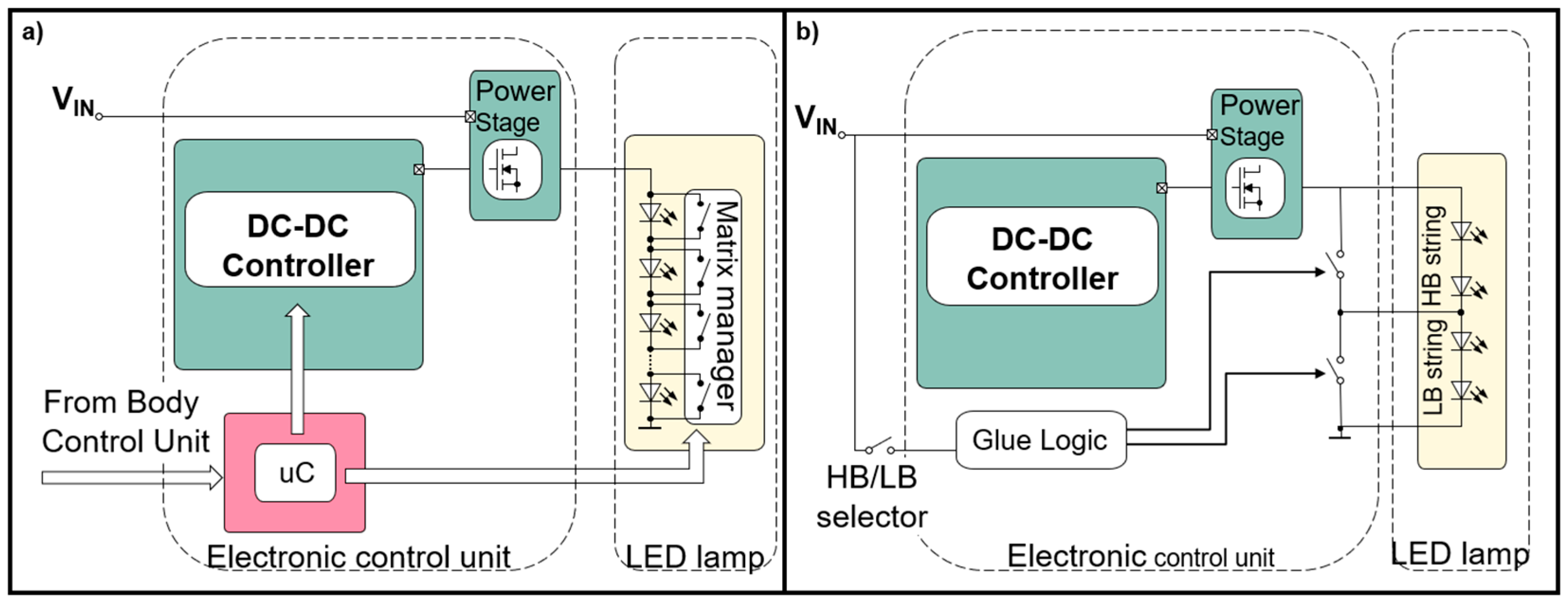
Since the power range for front-light applications requires at least 40 W [3,4], the need for DC-DC is the standard solution in the market to fulfill the overall system efficiency requirements. In Figure 1a, a glare-free front headlamp application realized with a combination of a power stage and a matrix manager controlled by a dedicated microcontroller is represented. The matrix manager device is a series of bypass switches with an adjustable slew rate [5] used to control the average current flowing in each LED of the string. Every single switch incorporates a dedicated PWM engine to adjust the average current from no current to the maximum allowable current from the DC-DC power stage that relies on a current control loop to regulate the current flowing through the LED string [6]. The intensity and the shape of the light beam are then managed by the commands sent by the microcontroller to the matrix manager device. In typical use cases, the system is connected to a 12 V battery, and the output voltage required to supply the LED string can vary from 2.5 V to more than 70 V [1,3] (depending on the number of LEDs the matrix manager is shorting). Considering the input/output voltages scenario, a buck–boost topology is necessary.
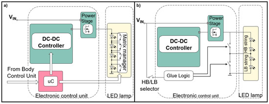
Figure 1.
Glare-free front headlamp application realized (a) with a combination of a power stage and a matrix manager controlled by a dedicated microcontroller and (b) for standard light functions such as HB and LB with switches in parallel.
Most LED drivers for HB (with three to five white LEDs) and LB (with five to eight LEDs) use a buck–boost DC-DC topology, which ensures that the desired output current is generated even during battery fluctuation (such as below 4 V during cold cranking or higher than 26 V during load dump) [4].
While these converters are effective in regulating power with static loads (high and/or low beams), they may struggle to maintain a constant current when the load is abruptly changed. In a DC-DC system, there is the potential for the matrix manager to dynamically short the LEDs in the string. This operation instantaneously reduces the forward voltage biasing of the entire load, causing the output capacitor (which is coupled in parallel to the load) to discharge. This generates a current spike through the LED string that has the potential to damage the remaining LEDs in the string [4].
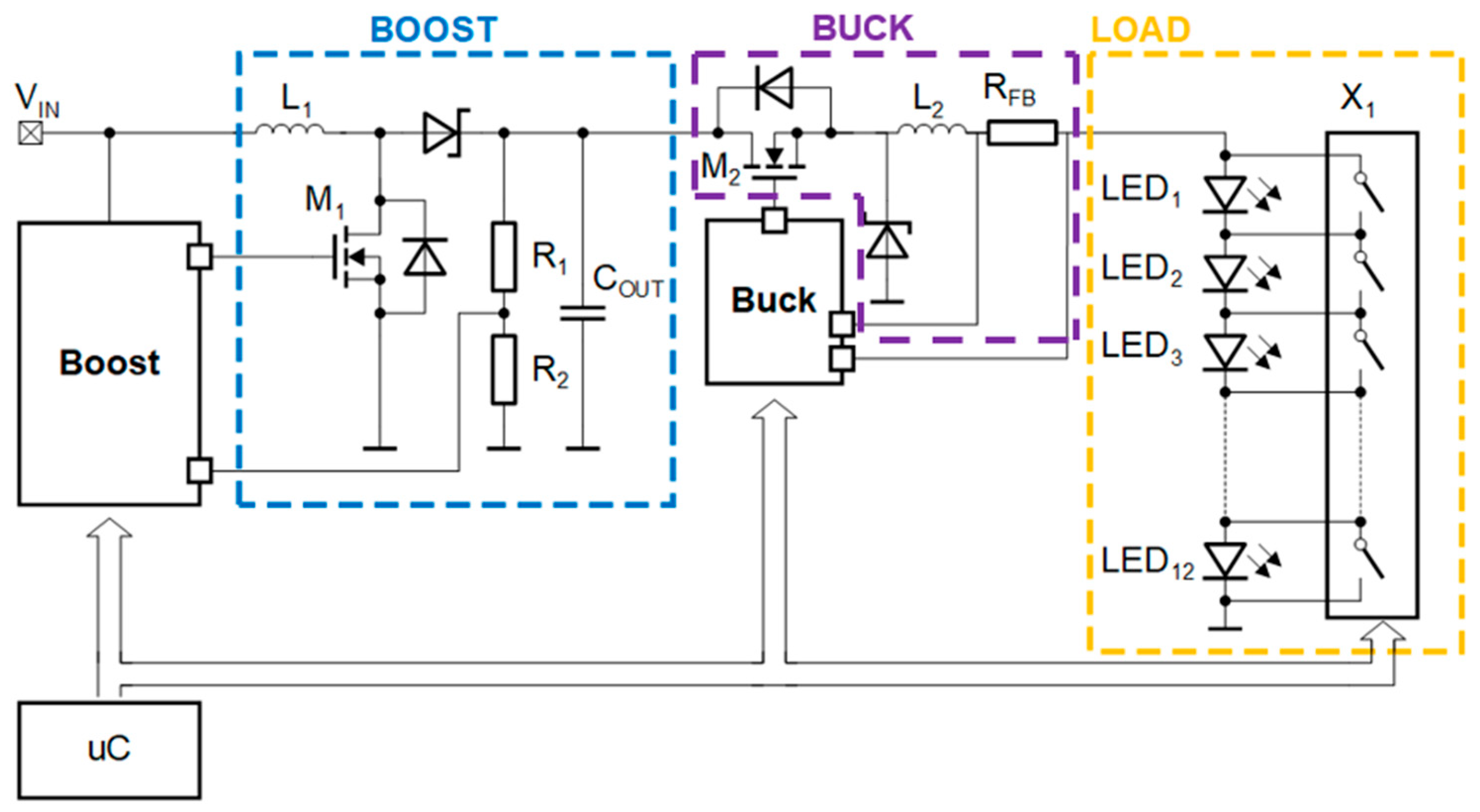
To overcome the issues mentioned earlier, various solutions have been adopted in the market, depending on the specific application case. For matrix lighting, the dual-stage boost + buck architecture is generally preferred [7,8,9]. In this solution, the high- and fixed-voltage boost stage supplies several higher-bandwidth buck stages. The buck stages have small output capacitors to minimize the current overshoots on the LED string during load variations. However, as one can see in Figure 2, this architecture involves two DC-DC converters and two DC-DC controllers, which results in higher system cost and lower overall efficiency.
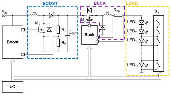
Figure 2.
Boost + buck architecture.
For standard light functions such as HB and LB (Figure 1b), a single buck–boost DC-DC is used to supply both LED strings. To save the system cost of an additional DC-DC, a bypass between the two light functions can be implemented using a switch in parallel to the portion of the LED string to be shorted. Current overshoots can be avoided by driving the turn-on phase of the switch as slowly as needed to match the limited bandwidth of the buck–boost regulator [10]. However, the function bypass switch must be driven at a slow speed, which puts severe constraints on the duty cycle of the single light function (duty cycle variation is used to adjust the LED light flux, without showing color shift in the generated light).
A solution that fits both applications and is based on a single buck–boost regulator has been adopted in [11]. In this case, the system overcomes the duty cycle limitation of the single DC-DC, showing, at the same time, high efficiency and low-cost applications. However, microcontroller supervision is needed to program the voltage steps in advance and to perform real-time calculations for timing optimization.
In this work, a new control system implemented with a single device to power dynamic adaptive lighting applications is presented.
2. System: Overview and Implementation
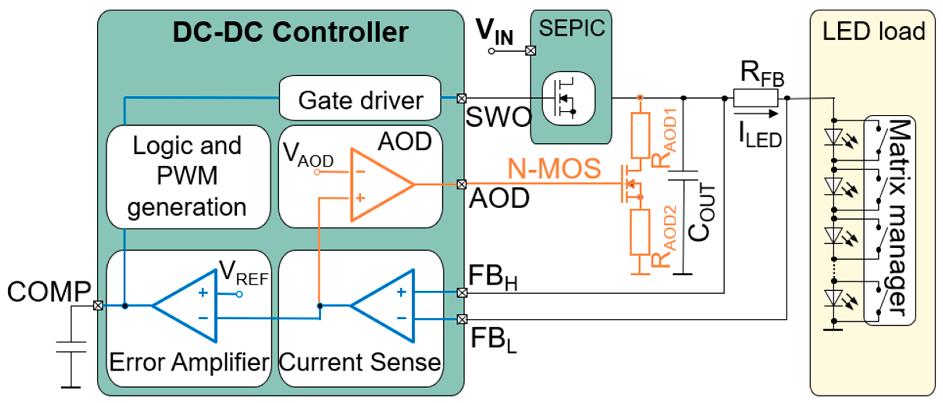
To enhance system efficiency, a single buck–boost regulator has been evaluated as an alternative to the dual-stage boost + buck architecture. In Figure 3, the proposed system [12] designed to address the previously identified limitations is illustrated. The system consists of (1) a dedicated device able to perform both the functions of a classical DC-DC controller and discharging path activation/deactivation, (2) a SEPIC power converter to achieve buck–boost regulation, (3) an NMOS switch with series limiting resistances to create a parallel path to ground and (4) the LED load. The power converter manages the current supplied to the LEDs, while the parallel NMOS switch dissipates current overshoots generated during load variations. During normal operation, this parallel adaptive output discharge (AOD) path remains deactivated.
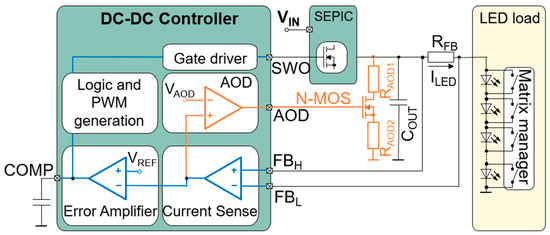
Figure 3.
System: DC-DC controller, SEPIC power converter, NMOS dumping element, limitation resistances, LED load with matrix manager, output capacitance COUT.
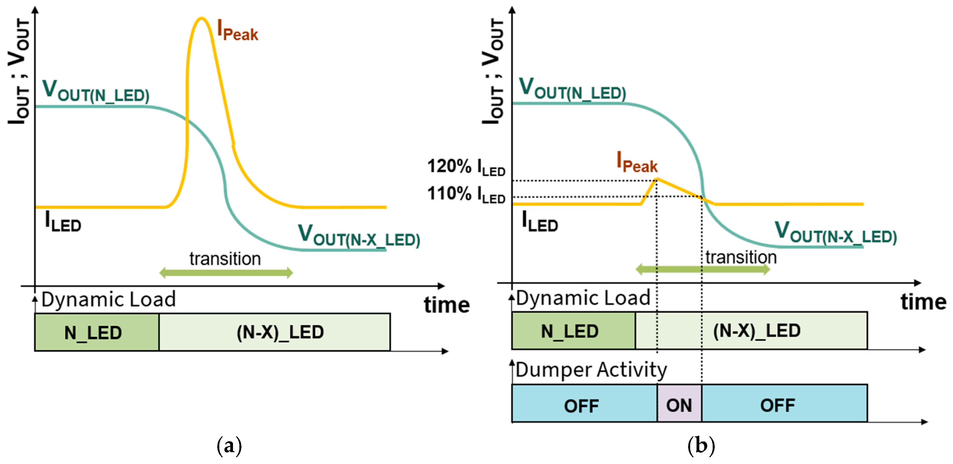
In Figure 4a,b, the system behavior with and without the discharging path is shown. Considering the case when no AOD path is present, when one or more LEDs are dynamically bypassed/shorted, the sudden decrease in the series resistance and the voltage drop in the load, consisting of the remaining LEDs in the string, causes a steep increase in the output current (Figure 4a) due to the discharging current coming from the output capacitance. In cases where the current overshoot exceeds the maximum rating, the LED could face permanent damage or a lifetime reduction. With the AOD feature, during the dynamic load transition, if the output current exceeds a predefined rising threshold—set at 120% of the target regulated current, as shown in the principle sketch in Figure 4b—the additional NMOS is activated by the controller, creating a parallel path to ground to dissipate the excess charge stored in the power converter output capacitor. In this way, the current flowing through the LEDs has been kept limited. The discharging path remains active until the output current drops below a predefined falling threshold—set at 110% of the target regulated current in the figure—at which point it is deactivated. The output voltage is dynamically adjusted to properly supply the LED string. The operation can occur once or multiple times for each load bypass until the required voltage is achieved. The number of activations is dependent on the bypass switch speed and the maximum discharge current allowed through the dumper NMOS, which determines the output capacitor discharge rate. To ensure system robustness and maintain LED reliability over time, i.e., to effectively limit the current spike, the discharge rate must exceed the speed of the bypass switches as a minimum requirement.
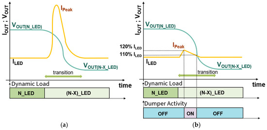
Figure 4.
System behavior: (a) ILED current peak, during dynamic load transition, without discharging path; (b) ILED current peak under control with active discharge.
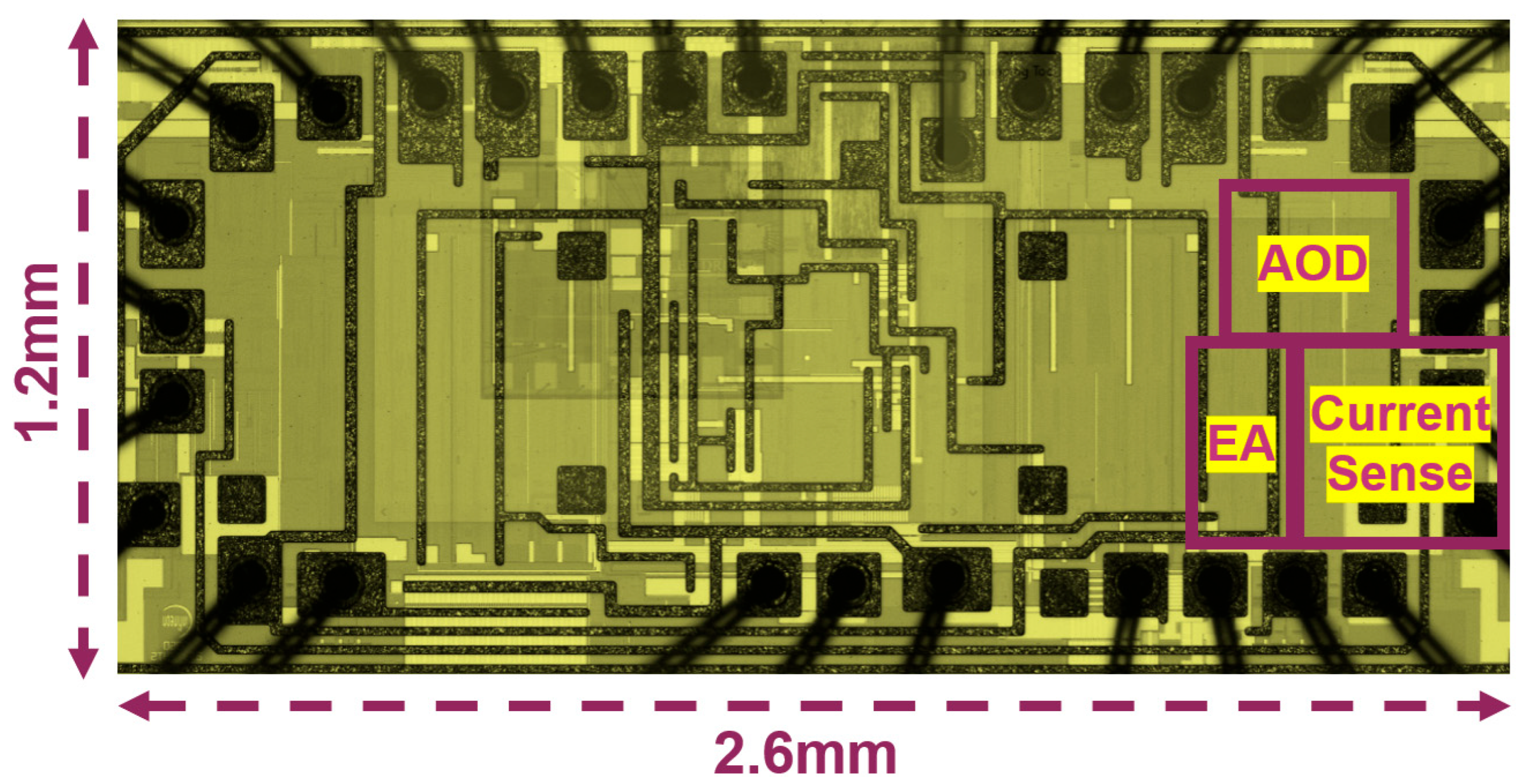
The proposed solution was implemented with a test chip fabricated in a 130 nm BCD technology by Infineon Technologies. A die micrograph is shown in Figure 5, where the main blocks have been highlighted. The key elements of the discharging path are as follows:

Figure 5.
Die micrograph. Dimensions and main blocks have been highlighted: error amplifier (EA), current sense and adaptive output discharge (AOD).
- The N-MOS dumping element in parallel to the output capacitance (COUT);
- The current sensing resistor (RFB) used to sense the output current;
- The NMOS current limiter resistor RAOD1,2.
In the system (Figure 3), the LED bypassing activity is detected sensing the output electrical current through the resistor RFB (also used for the regulation loop). The resistor is connected to the two test chip feedback pins FBH and FBL. The voltage signal across RFB is proportional to the flowing current (ILED). This signal is amplified by the internal current sense amplifier (CSA) and its output is connected to
- The error amplifier to close the control loop (blue parts in Figure 3);
- A comparator to manage the overcurrent events (orange parts in Figure 3).
Related to the overcurrent detection feature, the output voltage of the CSA is compared with the internal reference VAOD. When the output voltage of the CSA overcomes VAOD, the comparator output toggles to HIGH. The transition of this comparator consequently triggers N-MOS to turn ON, enabling the dumping path. Once the dumping element has been activated, the new path discharges the COUT, preventing the flowing of the extra current on the LEDs. To ensure the high reliability of the N-MOS, the current on the dumping path is limited by the presence of RAOD1,2, but, at the same time, the discharging path shall be fast enough to discharge the COUT faster than the bypass switch closure time. Furthermore, the reliability and thermal impedance of the MOSFET are very important aspects to be taken into consideration, and they will be deeply analyzed in the following paragraphs.
The blue-highlighted subcircuits are dedicated to the generation of the output current, although the current sense circuit can be considered part of both functionalities. The LED current (ILED) is detected by the CSA and compared with the Voltage Reference (VREF) of the current regulation loop. The error amplifier (EA) then produces a signal proportional to the difference between the VREF and the output of the current sense circuit. The difference at the error amplifier inputs is minimized by the control loop adjusting the switching activity at the Switching Output (SWO) via the pulse width modulation (PWM) engine and the gate driver. The regulation ensures that the target current is delivered to the load through the SEPIC converter. The output of the error amplifier is connected to the compensation pin (COMP), which is connected to an RC stability network to ensure proper system stability. When a switch in the matrix manager is closed, the DC-DC controller detects a sudden increase in output current. In response to this higher current, the error amplifier discharges the COMP node to compensate for the change [13]. Additionally, the device incorporates a peak current control mode to enhance stability performance [14].
The internal VAOD signal is used to define the current threshold that triggers the activation of the dumping element. This signal is derived as a function of the internal reference used for generating the output LED current (VREF). This approach reduces the process variation spread related to VAOD threshold in respect to the VREF. To ensure efficient capacitor discharge and to prevent continuous toggling of the comparator output, hysteresis has been added to the VAOD signal. When the load current reaches 120% of the target current (VAOD = 1.2 × VREF), the N-MOS is turned on by the device. Once the N-MOS is activated, the discharge of the output capacitance begins, and the internal VAOD is adjusted to lower the deactivation threshold to 110% of the target LED current (VAOD = 1.1 × VREF).
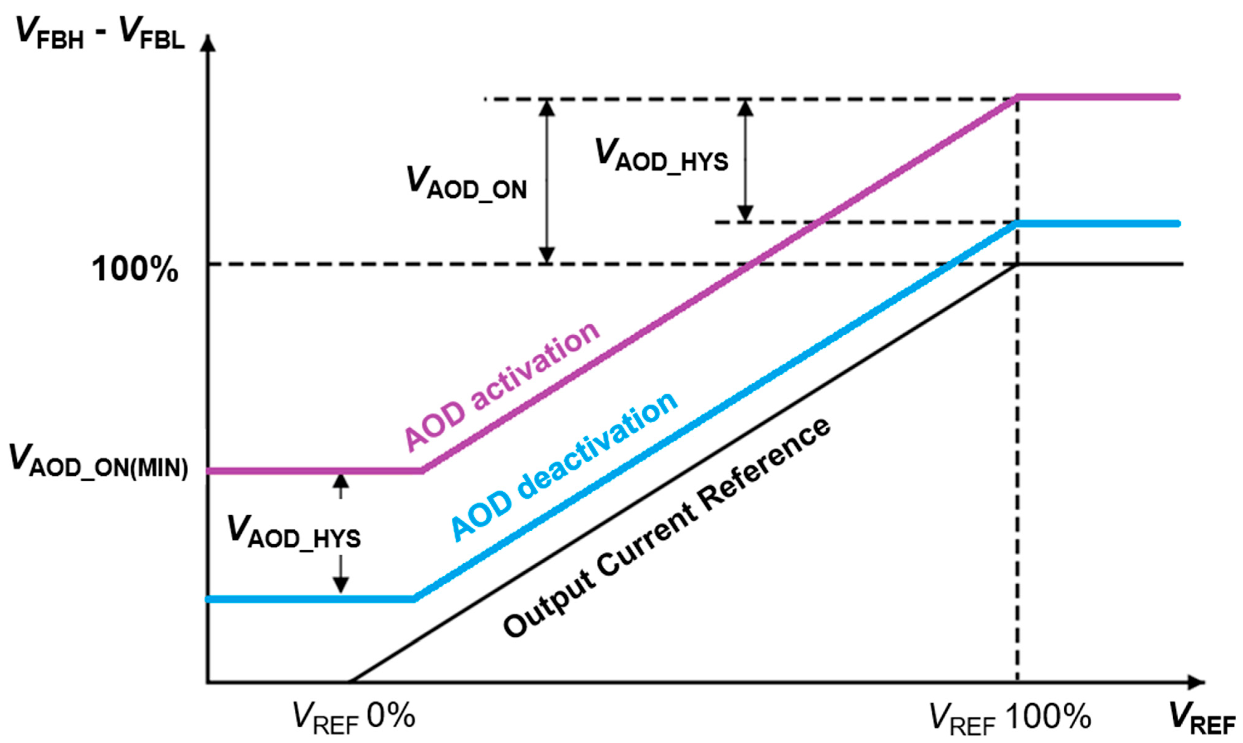
In Figure 6, the AOD activation and deactivation thresholds as functions of VREF are represented. The VREF signal is responsible for the regulated voltage VFBH–VFBL. The voltage drop across RFB (Figure 3) is proportional to the flowing current. An increase (decrease) in the VREF corresponds to an increase (decrease) in VFBH–VFBL and consequently an increase (decrease) in the output current, acting as an analog dimming.

Figure 6.
Adaptive output discharge (AOD) activation as function of VREF.
The adaptive output discharge activation threshold is modulated by the VREF down to a minimum reference voltage VAOD_ON(MIN) in order to reduce noise effects at low currents, while VAOD_HYS is the difference between the activation and deactivation thresholds corresponding to 10% of the reference voltage.
3. Experimental Results
The system was tested on a real test bench designed to emulate a glare-free high beam scenario, where the LED string was controlled by a matrix manager (Figure 7a). The matrix manager includes an adjustable slew rate, which can be configured through specific commands via the Serial Peripheral Interface (SPI) [5]. Typically, the slowest slew rate configuration is chosen to minimize electromagnetic emissions.
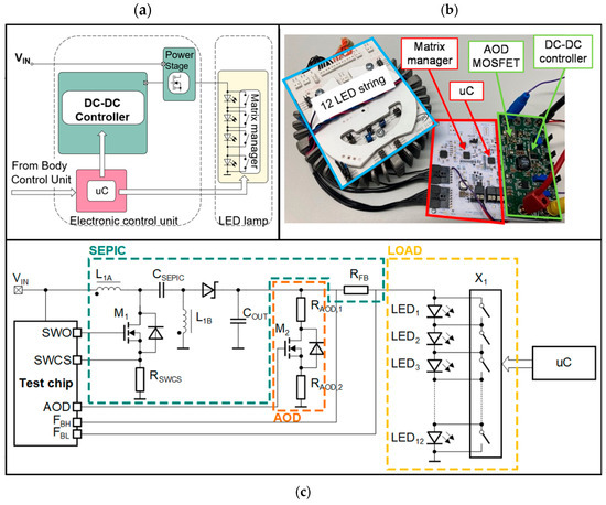
Figure 7.
Test bench implementation. In (a), the typical applicative case is sketched; in (b), the real test bench used in this work is shown, including the DC-DC, the matrix manager and the LED string; and in (c), the schematic with the main parts is represented.
In typical use cases, the DC-DC and the light source including the matrix manager are not on the same PCB [9]. In Figure 7b, the real measurement test bench used in this work is shown. The system is composed of the following:
- The LED load board;
- The DC-DC with an AOD feature;
- A board emulating the car body control unit, including the microcontroller.
In Figure 7c, the schematic with the main parts is represented. The DC-DC converter used in this work is a classical SEPIC topology. This is because the focus of this work was not related to the study of an innovative DC-DC converter, but it was mainly related to the use of the additional AOD feature in common applicative use cases. For this reason, a widely used DC-DC converter has been considered in this work. A SEPIC (Single-Ended Primary Inductor Converter) DC-DC converter is a power converter capable of stepping up (boosting) or stepping down (bucking) an input voltage to produce a regulated output voltage [15]. The SEPIC topology is widely used in applications where the input voltage can vary widely, such as battery-powered systems, automotive electronics, and renewable energy systems like solar energy harvesting [15,16,17,18]. It is especially useful in scenarios where the output voltage needs to remain constant regardless of whether the input voltage is higher or lower than the desired output. The key components are as follows:
- Input inductor (L1A): handles input current and stores energy during each switching cycle.
- Output Inductor (L1B): works together with the input inductor to manage current and energy transfer.
- Coupling Capacitor (CSEPIC): transfers energy between the input side and the output side while also isolating the two sides electrically.
- Switch (M1): provides the switching action to convert DC to a pulsed waveform.
- Diode: allows current to flow to the output during the switch-off period, preventing reverse current flow.
- Output Capacitor (COUT): smooths the output voltage to provide stable DC output.
In Figure 7c, the switching node current sense resistor RSWCS, used to detect the peak current through power switch M1, is also shown. The behavior of this function is outside of the scope of this work.
In Table 1, the values of the components used in the experimental setup described in Figure 7 are reported.

Table 1.
Values of components used in the experimental setup represented in Figure 7.
In this setup, the DC-DC converter regulates the LED current to 1.0 A, with each LED having a nominal forward voltage of 3.0 V at a junction temperature of 25 °C. This forward voltage decreases as the junction temperature rises [19]. During testing, the LED string operates at approximately 36 V. A 200 Hz PWM pattern is applied to the matrix manager, consisting of two scenarios: (1) continuous bypass and reconnection of nine LEDs in addition to three LEDs that remain always ON, and (2) continuous bypass and reconnection of six LEDs alongside six LEDs that are always ON. When LEDs are bypassed, a lower output voltage must be provided by the DC-DC converter. However, during this transition, a current spike in the LED string (ILED) is generated, discharging the output capacitor. The current spike, if not properly managed, can damage the LED.
To evaluate the performance of the proposed solution, experimental measurements have been performed both with and without the adaptive output discharge circuit enabled. If the adaptive output discharge circuit is disabled, the energy stored in the output capacitor and the primary inductor is discharged entirely into the LED string, even though the matrix manager employs a controlled slew rate for switching. This uncontrolled discharge highlights the risks to LED reliability in the absence of the adaptive discharge mechanism.
In this scenario, a peak current of 5 V is reached when a transition from 12 to 3 LEDs is performed, as shown in the yellow trace of Figure 8a. The figure also depicts the output voltage step (magenta curve) and the variation in the COMP voltage (compensation node) during the transition (blue curve). With all the LEDs active, the output voltage is obtained by the sum of the 12 LEDs’ forward voltage (VFWD ~3 V) and it is approximately 35/36 V. The exact voltage depends on the diode temperature, since the VFWD has a strong dependence on the temperature [19]. After the switching, only a portion of LEDs are still active, and the output voltage decreases depending on the number of the remaining LEDs. In Figure 8b, the same waveforms as in Figure 8a are presented, with the addition of the AOD (adaptive output discharge) signal shown in green. When the AOD feature is enabled, during the transition from higher to lower output voltage, the test chip effectively controls the output current, activating the discharging path every time the ILED is above the activation threshold and deactivating it when the current decreases below the deactivation threshold. In the specific case reported in Figure 8b, the AOD NMOS is activated 12 times to properly discharge the output capacitor, with the discharge current limited by the RAOD resistors. The current limitation ensures that the LED string is not overstressed during the lifetime. The system has undergone extensive testing across various use cases to validate its consistent performance and behavior. Figure 8c,d illustrate measurements for a transition from 12 LEDs to 6 LEDs.
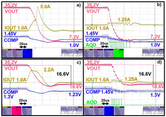
Figure 8.
Typical cases: (a,b) measurements with 12-to-3 LED transition w/o AOD enabled; (c,d) measurements with 12-to-6 LED transition w/o AOD enabled. (Note: IOUT division is 1 A with AOD disabled, while IOUT division is 500 mA with AOD enabled).
In Table 2, the performances of the proposed system with respect to state-of-the-art solutions are summarized. Four main aspects have been considered: (1) efficiency, referring to the system power conversion capability; (2) bandwidth, i.e., the system speed; (3) complexity, which takes into consideration the effort to properly set and size all the system parts (including software); and (4) cost. As one can see, in the proposed solution, the most relevant advantages rely on good performance in all the aspects associated with a low system cost.
Table 2.
Performance comparison with the proposed solution with respect to the state-of-the-art available systems.
The complexity of the AOD solution is mainly due to the sizing of the discharging path. For this reason, reliability aspects must be considered for the discharging NMOS and limiting resistors. This aspect is extensively analyzed in the following section.
4. AOD Discharging Path
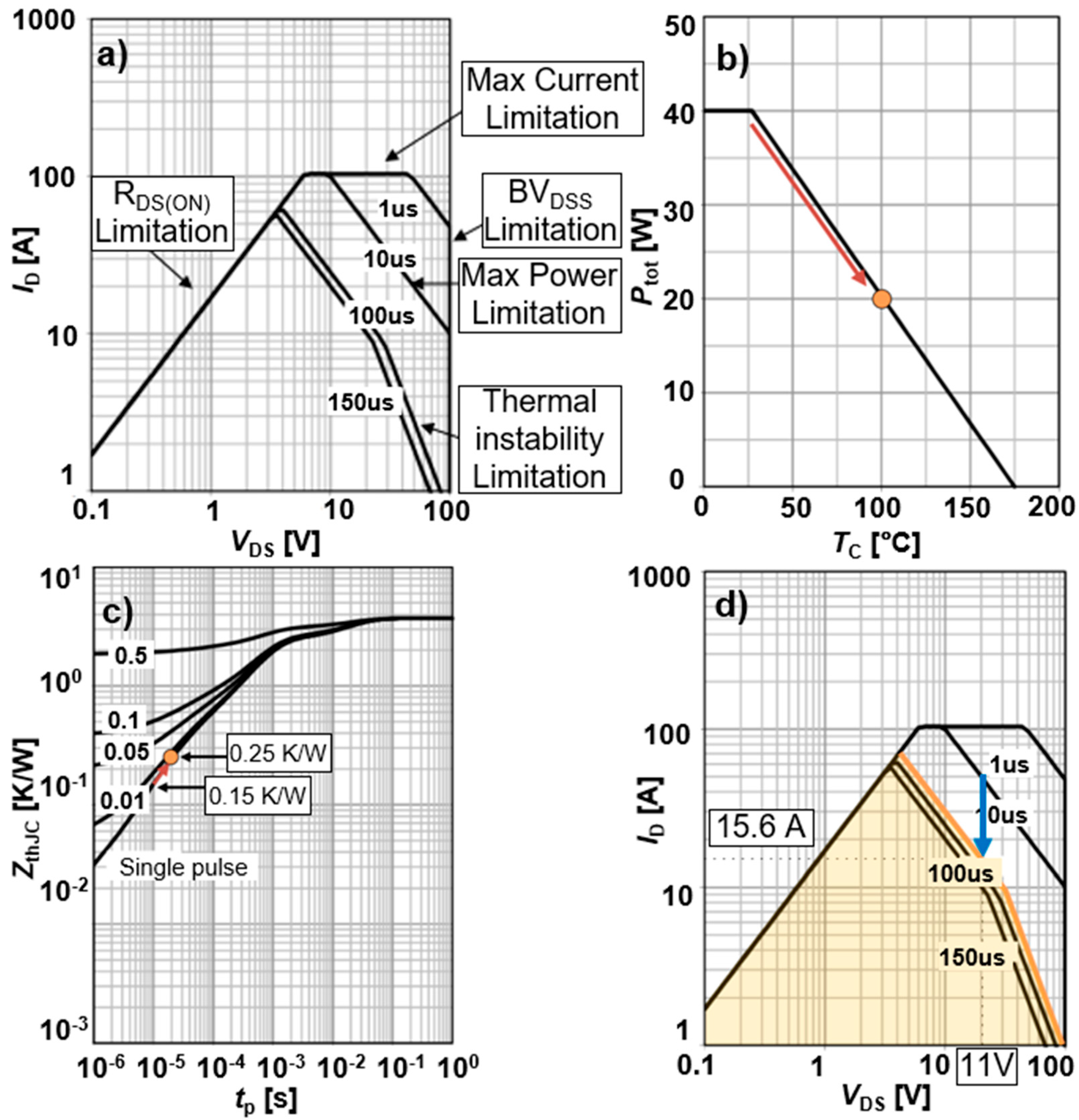
The dimensioning of the AOD discharging path is a key aspect to manage in order to obtain an efficient and reliable power dissipation during the current spikes. A critical aspect of this process is ensuring that the chosen NMOS operates within its Safe Operating Area (SOA) to avoid thermal runaway or device failure. The SOA chart serves as a guide to define the safe operating conditions for a MOSFET, thus preventing possible damage. For example, Figure 9a illustrates the SOA for a typical MOSFET such as the IAUC26N10S5L245 [20]. The chart is divided into several distinct regions, each representing a specific operational limit: (1) RDS(ON) limitation: this region represents the current limit imposed by the MOSFET’s drain–source on-resistance (RDS(ON)), as per Ohm’s law, with the relationship given by ID = VDS/RDS(ON); (2) maximum current limitation: this limit defines the absolute maximum drain current (ID) the MOSFET can handle, beyond which damage may occur; (3) maximum power limitation: this boundary marks the highest power the MOSFET can dissipate while maintaining junction temperatures within safe limits; (4) thermal instability limitation: representing the onset of thermal instability, these lines indicate regions where localized overheating could lead to device failure, also known as secondary breakdown; and (5) BVDSS breakdown limitation: this limit specifies the maximum voltage the MOSFET can withstand without entering breakdown, ensuring safe operation below this threshold.

Figure 9.
(a) IAUC26N10S5L245 SOA; (b) power dissipation chart; (c) transient thermal resistance; (d) derated SOA.
The standard SOA characteristics are typically provided for an ambient temperature of 25 °C and under single-pulse applications. However, these conditions represent ideal scenarios that are not always practical in applications with higher ambient temperatures or pulsed power applied. In these cases, the SOA needs to be derated to ensure the MOSFET’s reliability and lifespan, thus compensating for the reduced power dissipation capability and the increased transient thermal resistance arising when operating conditions are not the ideal ones. To properly assess derating, two additional graphs are needed: (1) the power dissipation chart, which illustrates the device heat dissipation capacity under steady-state conditions across various ambient temperatures (Figure 9b), and (2) the transient thermal resistance chart, which represents the thermal impedance of the package during dynamic conditions, such as varying pulse durations and repetition rates (Figure 9c). The transient thermal resistance chart highlights how pulse duration and repetition rate influence the heat dissipation performance. For instance, in an ADB system, the discharge phase of the output capacitance, consisting of a few (3–4) pulses each lasting 3–4 µs with a 10 ms repetition rate, can be approximated to a single 20 µs pulse. In this scenario, the transient thermal impedance (ZthJC) may degrade by a factor of 1.6 (increasing from 0.15 K/W to 0.25 K/W) when compared to the 10 µs single-pulse curve indicated on the SOA chart.
The power dissipation chart (Figure 9b) illustrates the impact of the ambient temperature on the dissipation capability of the considered MOSFET. In automotive front-lighting systems, temperature can reach up to 105 °C and, in these conditions, the power dissipation capability is reduced by half, dropping from 40 W at 25 °C to 20 W at 105 °C. When combining the effects of higher ambient temperature with longer pulse duration, the effective power dissipation capability is further reduced by a derating factor (DF) of 3.2—a factor of 2 due to limited power dissipation and a factor of 1.6 due to changes in transient thermal impedance (ZthJC).
To create an updated SOA chart, a reference point from the original power dissipation curve must be taken. For example, at a junction temperature of 25 °C, the device can handle a single-pulse current of 50 A with a source-to-drain voltage drop of 11 V, resulting in a peak power of 550 W. When factoring in longer pulse durations and the higher ambient temperature, this peak power is recalculated as follows:
PPEAK_NEW = PPEAK_ORIGINAL/DF = 550 W/3.2 = 171.9 W.
This new power limit at VDS = 11 V is achieved with a current equal to
IPEAK = PPEAK_NEW/VDS = 171.9 W/11 V = 15.6 A.
The updated current limit, adjusted to reflect the new peak power constraint, is derived by shifting the original limit downward to cross the new boundary at the recalculated values. The modified SOA region is highlighted in orange in Figure 9d.
Considering the specific case depicted in Figure 7c, a crucial role in establishing an upper limit for the current flowing through the MOSFET (M2) during the discharge process is played by the limiting resistance RAOD2. At the same time, to reduce the thermal stress on M2, RAOD1 is sized to reduce the power amount on M2, thus sharing the power dissipation between the resistance and the MOSFET. The peak of the discharging current in the AOD path is defined by the MOSFET thermal capability and the duration of the current pulse. In this work, a peak current of ID = 15.6 A has been considered.
To determine the suitable RAOD2 value, the following key parameters must be considered: (1) AOD gate driver output voltage: this is the voltage provided by the test chip to the MOSFET gate, determining its switching between ON and OFF states; and (2) MOSFET Threshold Voltage (Vth): this represents the minimum gate-to-source voltage required to transition the MOSFET from its OFF state to its ON state. Using these two parameters, the value of RAOD2 can be calculated as follows:
RAOD2 = (VAOD − VTH)/ID = (5 V − 1.7 V)/15.6 = 0.21 Ω.
RAOD1 is intended to maintain the MOSFET within the SOA during operation. For example, with ID = 15.6 A, the considered MOS [20] can manage a VDS up to 11 V considering the revised SOA. Considering a maximum output voltage (VOUT,max) equal to 50 V (depending on the maximum output voltage related to the application), RAOD1 can be calculated using the following relationship:
RAOD1 = [(VOUT_max − VDS) − (VAOD − VTH])/IPEAK = [(50 V − 11 V) − (5 V − 1.7 V)]/15.6 = 2.29 Ω.
This calculation ensures that the MOSFET operates within its derated SOA, considering the elevated temperature and the pulsing scenario.
5. Conclusions
In this work, a cost-effective solution for driving a dynamic LED string using a single DC-DC converter/controller has been presented. Based on existing features of a standard DC-DC converter for LED applications—such as the current sense circuit and the driving stage—adding few additional external components to create a discharge path, the proposed solution has been achieved. The LED current is monitored and compared with a defined threshold. The activation of a dumping element prevents current spikes that could reduce the LEDs’ lifespan. Proper power management of the discharge path is crucial, since the output voltage of the DC-DC converter decreases proportionally to the number of bypassed LEDs. Consequently, larger LED transitions require the discharge path to dissipate more power. Experimental data confirm that the system reacts to a fast change in the LED load limiting the current spikes. Although the proposed solution exhibits good performances in terms of efficiency, speed and system cost, some drawbacks need to be considered. First, the peak discharge current is a key parameter, defining the power handling and dissipation within the system. The correct sizing of the discharging path is crucial for the system reliability. The two limiting resistors play a fundamental role in fixing the peak current and in offloading the power to be dissipated by the NMOS. The operational integrity of the MOSFET within the Safe Operating Area is a critical consideration to be carefully evaluated. Furthermore, the device has been designed to manage fast discharges, but no strategy has been implemented for a fast charging phase. In these phases, the system reacts with the limited bandwidth of the DC-DC. To this end, an intelligent management of the COMP node can be considered to improve the performances in terms of speed.
Author Contributions
Conceptualization, P.L., F.B., M.G., R.P., E.T. and E.B.; methodology, P.L., F.B., R.P., E.T. and M.G.; formal analysis, P.L., F.B. and E.B.; investigation, P.L., F.B. and E.B.; resources, M.G. and F.B.; data curation, P.L. and F.B.; writing—original draft preparation, P.L.; writing—review and editing, P.L., F.B., R.P., E.T. and M.G.; supervision, M.G. All authors have read and agreed to the published version of the manuscript.
Funding
This research received no external funding.
Institutional Review Board Statement
Not applicable.
Informed Consent Statement
Not applicable.
Data Availability Statement
The original contributions presented in this study are included in the article. Further inquiries can be directed to the corresponding author.
Conflicts of Interest
The authors declare no conflicts of interest.
Glossary
The following abbreviations are used in this manuscript:
| AOD | Adaptive Output Discharge: Feature that activates a discharging path to prevent current spikes in the LED string during dynamic load transitions. |
| BVDSS | Breakdown Voltage: Maximum voltage that a MOSFET can withstand without entering breakdown. |
| CSA | Current Sense Amplifier: Amplifier used to sense the output current of the DC-DC converter. |
| DC-DC | Power converter that converts a DC input voltage to a DC output voltage. |
| DF | Derating Factor: used to reduce the power dissipation capability of a MOSFET due to higher ambient temperatures or longer pulse durations. |
| DRL | Daytime Running Light: Feature that allows a vehicle’s headlights to be on during the daytime to increase visibility and safety on the road. |
| EA | Error Amplifier: Amplifier used to regulate the output current of the DC-DC converter. |
| EMC | Electromagnetic Compatibility: The ability of a device to operate in its electromagnetic environment without causing or suffering from electromagnetic interference. |
| FBH–FBL | Feedback Pins: Pins used to sense the output current of the DC-DC converter. |
| HB | High Beam: Setting of vehicle headlight beam with a long-range focus. |
| LB | Low Beam: Setting of vehicle headlight beam with a short-range focus. |
| LED | Light Emitting Diode: Semiconductor device that emits light when an electric current passes through it. |
| OEM | Original Equipment Manufacturer: Company that manufactures vehicles or vehicle components, such as engines, transmissions, or electronics, that are used in the production of vehicles by other companies. |
| PPEAK | Peak Power: The maximum power that a MOSFET can dissipate during a pulse. |
| PWM | Pulse Width Modulation: Technique used to control the average current flowing in each LED of the string. |
| RAOD1,2 | Limiting Resistances: Resistors used to limit the current flowing through the MOSFET during the discharge process. |
| SEPIC | Single-Ended Primary Inductor Converter: Type of DC-DC converter that can step up or step down the input voltage to produce a regulated output voltage. |
| SOA | Safe Operating Area: Region of operation for a MOSFET that ensures its reliability and lifespan. |
| SPI | Serial Peripheral Interface: Interface used to configure the matrix manager. |
| VFWD | Forward Voltage: The voltage drop across an LED when it is forward-biased. |
| VREF | Voltage Reference: Reference voltage used to regulate the output current of the DC-DC converter. |
| VTH | Threshold Voltage: The minimum gate-to-source voltage required to transition a MOSFET from its OFF state to its ON state. |
| ZthJC | Transient Thermal Impedance: Measure of the thermal impedance of a package during dynamic conditions. |
References
- Yole. Automotive Lighting, Innovation, and New Functionalities Are Spreading Across Front, Rear, and Interior Applications, Pushing the Market to $42.5B in 2027. 2022. Available online: https://www.yolegroup.com/product/report/lighting-for-automotive-2022/ (accessed on 25 January 2025).
- Strategy Analytics. Who is Influencing the Automotive Ecosystem? 2021. Available online: https://www.strategyanalytics.com/strategy-analytics/blogs/automotive/autonomous-vehicles/autonomous-vehicles/2022/09/22/who-is-influencing-the-automotive-ecosystem (accessed on 25 January 2025).
- Chowdhury, M.S.A.; Rahman, A.M. Electric efficiency of the lighting technology of auto industry: Recent development and future prospect. In Proceedings of the 2016 4th International Conference on the Development in the in Renewable Energy Technology (ICDRET), Dhaka, Bangladesh, 7–9 January 2016; pp. 1–5. [Google Scholar] [CrossRef]
- Infineon Technologies. Reference Design for High Beam and Low Beam Combination Using TLD5099EP. 2020. Available online: https://www.infineon.com/cms/en/product/evaluation-boards/ledfronthblb_ref/ (accessed on 25 January 2025).
- Texas Instruments. TPS92663-Q1 High-Brightness LED Matrix Manager for Automotive Headlight Systems. 2018. Available online: http://www.ti.com/lit/ds/symlink/tps92663-q1.pdf (accessed on 20 May 2025).
- Hu, Y.; Jovanovic, M.M. LED Driver with Self-Adaptive Drive Voltage. IEEE Trans. Power Electron. 2008, 23, 3116–3125. [Google Scholar] [CrossRef]
- Fărcaș, C.; Petreuș, D. LED Driver with BOOST-BUCK Topology. In Proceedings of the 2021 44th International Spring Seminar on Electronics Technology (ISSE), Bautzen, Germany, 5–9 May 2021; pp. 1–5. [Google Scholar] [CrossRef]
- Mukherjee, S.; Sepahvand, A.; Yousefzadeh, V.; Doshi, M.; Maksimović, D. A Two-Stage Multiple-Output Automotive LED Driver Architecture. In Proceedings of the 2020 IEEE Energy Conversion Congress and Exposition (ECCE), Detroit, MI, USA, 11–15 October 2020; pp. 1492–1498. [Google Scholar] [CrossRef]
- Texas Instruments. 120W Dual-Stage Matrix Compatible Automotive Headlight: ECU Reference Design. 2019. Available online: https://www.ti.com/lit/ug/tidueu1a/tidueu1a.pdf?ts=1748261584404&ref_url=https%253A%252F%252Fwww.ti.com%252Ftool%252FTIDA-050030 (accessed on 20 May 2025).
- Szolusha, K.; Lawrence, K. One LED Driver Is All You Need for Automotive LED Headlight Clusters. 2015. Available online: https://www.analog.com/media/en/technical-documentation/tech-articles/lt-journal-article/ltjournal-v25n2-03-df-lt3795_lt3952-keithszolusha.pdf (accessed on 25 January 2025).
- Penzo, R.; Galvano, M.; Milanesi, P.; Capodivacca, G. Buck-Boost Converter with Active Output Voltage Discharge. US9203311B2, 1 December 2015. Available online: https://patentimages.storage.googleapis.com/55/06/31/d8852a24d19edb/US9203311.pdf (accessed on 25 January 2025).
- Lorenzi, P.; Borghetti, F.; Penzo, R.; Bezzati, E.; Tonazzo, E.; Galvano, M. Adaptive Output Discharge DC-DC for glare free LED front-light. In Proceedings of the ESSCIRC 2023—IEEE 49th European Solid State Circuits Conference (ESSCIRC), Lisbon, Portugal, 11–14 September 2023; pp. 237–240. [Google Scholar]
- Infineon Technologies. LITIX™ Power TLD6098-2ES. 2024. Available online: https://www.infineon.com/dgdl/Infineon-Infineon-TLD6098-2ES-DS_v01_10-EN-DataSheet-v01_20-EN.pdf?fileId=8ac78c8c7d0d8da4017d3a67cb5d351b (accessed on 20 May 2025).
- Ridley, R.B. A new Continuous Time Model for Current Mode Control. IEEE Trans. Power Electron. 1991, 6, 271–280. [Google Scholar] [CrossRef]
- Verma, M.; Kumar, S.S. Hardware Design of SEPIC Converter and its Analysis. In Proceedings of the 2018 International Conference on Current Trends Towards Converging Technologies (ICCTCT), Coimbatore, India, 1–3 March 2018. [Google Scholar]
- Chiang, S.J.; Shieh, H.-J.; Chen, M.-C. Modeling and Control of PV Charger System With SEPIC Converter. IEEE Trans. Ind. Electron. 2009, 56, 4344–4353. [Google Scholar] [CrossRef]
- PMaroti, K.; Padmanaban, S.; Holm-Nielsen, J.B.; Bhaskar, M.S.; Meraj, M.; Iqbal, A. A New Structure of High Voltage Gain SEPIC Converter for Renewable Energy Applications. IEEE Access 2019, 7, 89857–89868. [Google Scholar] [CrossRef]
- Ma, H.; Lai, J.-S.; Feng, Q.; Yu, W.; Zheng, C.; Zhao, Z. A Novel Valley-Fill SEPIC-Derived Power Supply Without Electrolytic Capacitor for LED Lighting Application. IEEE Trans. Power Electron. 2012, 27, 3057–3071. [Google Scholar] [CrossRef]
- Nichia. Thermal Design Considerations for Nichia NVSW719AC LEDs. 2023. Available online: https://led-ld.nichia.co.jp/api/data/spec/tech/SP-QR-C2-230307-1-E_Thermal%20Design%20Considerations%20for%20the%20Nichia%20NVSW719AC%20LEDs.pdf (accessed on 20 May 2025).
- Infineon Technologies. IUAC26N10S5L245 Datasheet. Available online: https://www.infineon.com/dgdl/Infineon-IAUC26N10S5L245-DataSheet-v01_01-EN.pdf?fileId=5546d46279cccfdb0179ccd3ea760202 (accessed on 20 May 2025).


Disclaimer/Publisher’s Note: The statements, opinions and data contained in all publications are solely those of the individual author(s) and contributor(s) and not of MDPI and/or the editor(s). MDPI and/or the editor(s) disclaim responsibility for any injury to people or property resulting from any ideas, methods, instructions or products referred to in the content. |
© 2025 by the authors. Licensee MDPI, Basel, Switzerland. This article is an open access article distributed under the terms and conditions of the Creative Commons Attribution (CC BY) license (https://creativecommons.org/licenses/by/4.0/).