1. Introduction
Inkjet printing technology has been widely applied across numerous industrial fields. Traditionally, inkjet printing was primarily used in graphic arts and publishing sectors. However, in recent years, its applications have been continuously expanding into emerging areas such as electronics [
1], pharmaceuticals [
2], and materials science [
3]. This technology achieves high-precision and high-efficiency generation of images and patterns by accurately ejecting tiny droplets onto substrates, and is therefore widely regarded as a manufacturing process with immense potential [
4].
One of the key components of an industrial inkjet printing system is the printhead, whose performance directly affects printing accuracy, speed, and reliability [
5]. The drive waveforms of the printhead can be classified into unipolar [
6,
7] and bipolar [
8,
9] types based on their polarity. Unipolar waveforms include M-shaped [
10] and W-shaped [
11] waveforms, while bipolar waveforms are further subdivided into N-shaped [
12], M-shaped [
13], W-shaped, and other complex waveform types. Even within the same type of waveform, variations in parameters such as rise time, dwell time, and fall time can significantly impact the jetting performance of piezoelectric inkjet printheads [
14]. The selection of drive waveforms is closely related to the specific application scenarios of the printhead [
15,
16,
17]. Different application scenarios impose varying requirements on printing accuracy, speed, as well as the size and shape of ink droplets. Therefore, it is essential to generate corresponding drive waveforms to meet these diverse needs.
In complex heterogeneous material printing scenarios (a concept distinct from heterogeneous printing in 3D printing [
18,
19,
20], such as printing on paper greeting cards with velvet patches, garments made from multiple fabrics, and plastic suitcases with metal components), printing on substrates made from different materials requires specialized technologies, such as pre-coating surface preparation [
21], digital direct to garment (DTG) printing technology [
22], and UV-LED curing technology [
23]. These technologies, in addition to inkjet printing, often require additional substrate treatment or the assistance of other equipment, leading to higher costs.
In industrial printhead applications, the design of drive waveforms faces numerous challenges [
24,
25,
26,
27]. The adjustability of the waveform is a critical consideration. In heterogeneous material printing scenarios, substrates made of different materials have varying requirements for droplet size, speed, and shape. Therefore, the waveform generation system must exhibit a high degree of flexibility to quickly switch between different waveform configurations based on the substrate.
We have compiled a list of mainstream printing systems on the market, as shown in
Table 1, all of which lack the ability to quickly switch waveforms based on different substrates.
To address the above issues, this paper proposes a low-cost solution for heterogeneous material printing scenarios. While current industrial printhead controllers support online updates of driving waveform parameters to accommodate different materials, they typically require interrupting the printing process or reloading control commands, failing to achieve real-time waveform switching during continuous printing. This limitation significantly hinders dynamic multi-material printing and frequent surface treatment applications.
We have designed and implemented an FPGA-based waveform generation system with rapid switching capability, which enables flexible generation of various drive waveforms through a triple-array description method. More importantly, the proposed system can perform real-time waveform switching according to preset logic without interrupting printing tasks—a critical advancement for dynamic adaptation to heterogeneous material surfaces. Through efficient memory layout and block random access memory (BRAM) read mechanisms, our system pioneers seamless switching between multiple material interfaces during continuous printing, overcoming the limitations of existing solutions.
Experimental results validate that the system not only offers high flexibility and precision but also meets complex printing scenario demands. The demonstrated real-time switching capability holds substantial engineering value for industrial inkjet applications, providing a novel solution beyond conventional approaches.
2. Control Principle of Proposed System
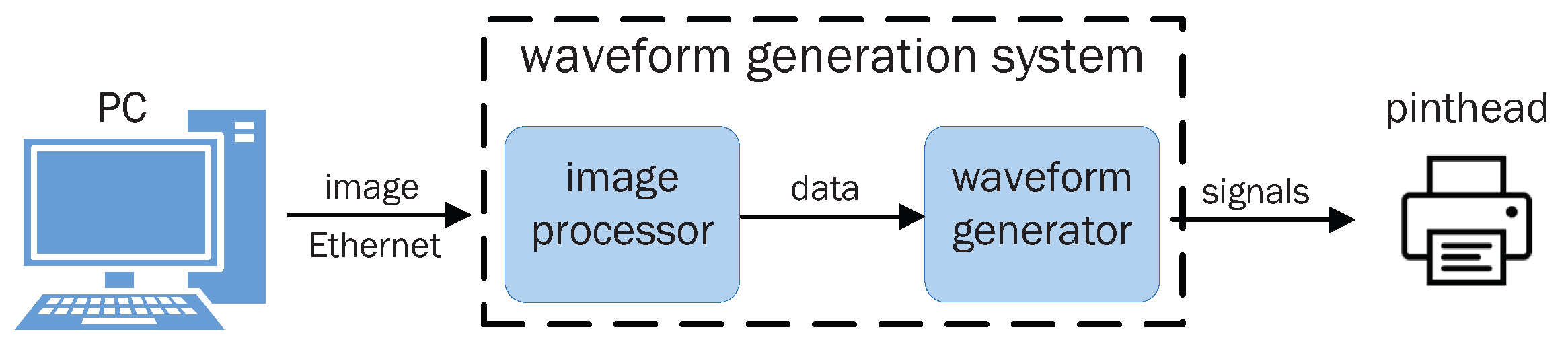
The process by which the proposed waveform generation system drives inkjet printing of an industrial printhead is shown in
Figure 1. The PC sends the image to be printed to the waveform generation system via Ethernet. The image processor within the waveform generation system processes the image into specific data and sends them to the waveform generator. The waveform generator processes these data and generates drive signals for the industrial printhead to perform inkjet printing.
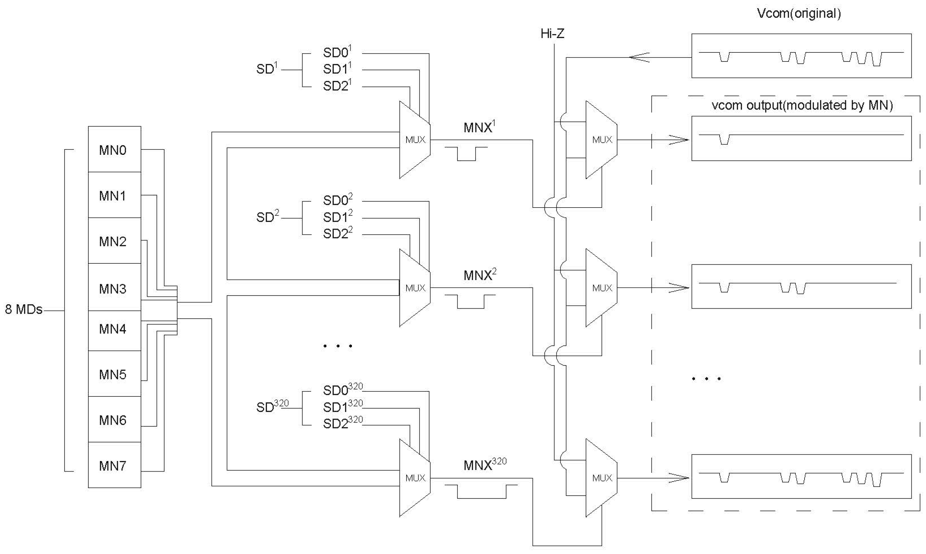
The principle by which the system controls the selection of inkjet drive waveforms for the printhead nozzles is illustrated in
Figure 2 (the principle of waveform switching will be introduced in subsequent chapters). This figure depicts one typical printhead drive waveform selection mechanism for a column of 320 nozzles. SD0, SD1, and SD2 constitute the 3-bit pixel waveform selection signal (SD) for an individual nozzle, which selects one of the eight driving waveforms, while MN0 through MN7 represent a continuous 8-bit inkjet control signal (MD) that picks parts of the vcom signal to form one driving waveform. Superscripts are used to distinguish the signals for each nozzle. The SD signal for each nozzle selects the corresponding MNX (one of MN0 to MN7), and when MNX is in a low state, the vcom inkjet drive waveform is selected to drive the printhead nozzle; otherwise, it outputs a high-impedance state. The pixel waveform selection signal SD, the inkjet control signal MD, and the inkjet drive waveform vcom are all derived from the processing for the image to be printed.
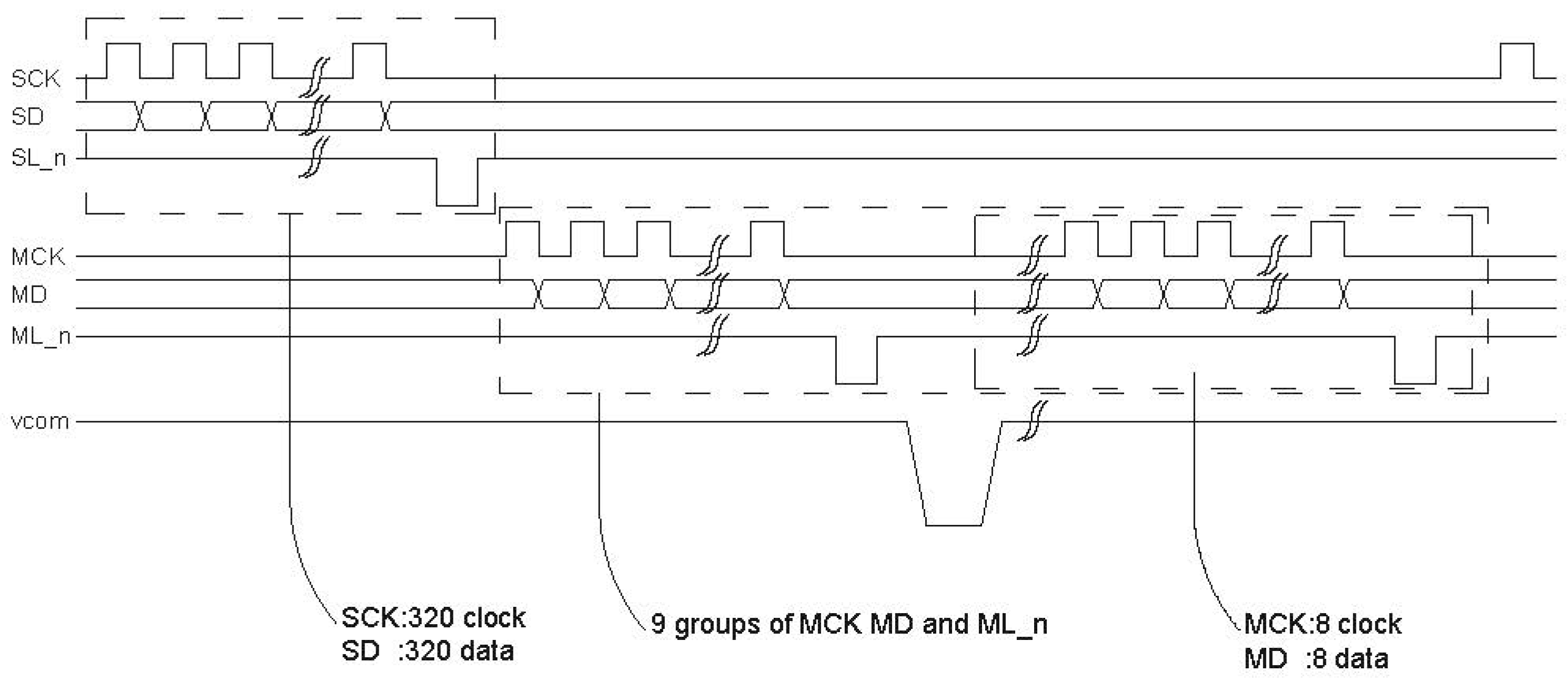
To ensure that the printhead correctly receives the SD and MD signals, it is necessary to provide not only the SD, MD, and vcom signals but also the corresponding clock and latch signals. The clock signal used to control the SD signal is called SCK, and SD’s latch signal is SL_n. Similarly, the clock signal used to control the MD signal is called MCK, and MD’s latch signal is ML_n. Both SL_n and ML_n are active-low signals. The timing relationships of these signals are illustrated in
Figure 3, which shows the timing sequence for printing one column of 320 nozzles. First, 320 pixel selection signals (SD) are shifted in and latched. Then, the first group of MD signals is used to preheat the nozzles. This is followed by eight successive groups of MD signals, each selecting a specific vcom waveform to control the size of the ejected droplet or to inhibit ejection. Together, these eight waveform selections constitute a complete printing cycle.
3. Proposed Waveform Generation System
3.1. Overview
Based on the aforementioned waveform control principles, we have designed a printhead waveform drive generation system that is capable of generating drive signals for the printhead and can switch between different waveforms at any time. The system’s hardware platform consists of a ZYNQ-7020 development board and a MAX5183 digital-to-analog converter (DAC) chip. The ZYNQ-7020 development board integrates the features of programmable logic and an ARM processor, providing a flexible and efficient hardware design space; meanwhile, the MAX5183 DAC is responsible for accurately converting digital signals into analog signals.
The framework of the system is illustrated in
Figure 4. It comprises an ARM core, DDR3 memory, an FPGA chip, and a DAC chip. The ARM is responsible for processing images, generating pixel waveform selection data, inkjet control data, and inkjet drive waveform data, as well as controlling the waveform generation process. DDR3 memory is used to store these data. We implement the core logic for generating the aforementioned signals within the FPGA. The DAC chip converts the digital signals generated by the FPGA into analog signals. Communication between the ARM, DDR3 memory, and FPGA is carried out via the AXI bus.
In the FPGA, we have divided the required functionalities into six modules, as shown in
Figure 4. Modular design allows for the free combination and customization of modules to accommodate different printheads. The SGenerator module generates the SCK, SD, and SL_n signals. The MGenerator is responsible for generating the MCK, MD, and ML_n signals. The VGenerator handles the generation of intermediate signals required by the DAC and, together with the DAC, produces the vcom signal that drives the printhead after being modulated by MN signals; this module also supports the system’s generation of eight various waveforms. The Registers module serves as the interface between the waveform generation system and the software, recording and maintaining various status and configuration information. The accessMem module provides data for waveform generation while ensuring rapid switching between waveforms. The PLL supplies different clock signals to the aforementioned modules. We utilize vivado’s IP cores to implement the PLL. Next, we will introduce the specific implementations of the first five modules.
3.2. SGenerator and MGenerator Modules
The SGenerator module generates the SCK, SD, and SL_n signals, while the MGenerator module generates the MCK, MD, and ML_n signals. The generation logic for both sets of signals is very similar (as shown in
Figure 3). The signal generation process for both follows these steps: first, a certain number of clock pulses are generated; then, a latch signal is produced; next, the system waits for a specified period; and this process is repeated a number of times until completion. It is important to note that the bit widths of the SD and MD signals differ. To uniformly handle these two types of signals, we designed a general XGenerator module, which parameterizes the number of pulse signals, waiting time, number of repetitions, and signal bit width. The SGenerator and MGenerator modules can be instantiated from the XGenerator module by simply setting the appropriate parameters according to specific requirements. Since industrial printheads have a maximum input clock frequency limit, we selected the SCK and MCK clock frequencies to be 30 MHz. Additionally, to ensure that all signals within the module reside in the same clock domain, the driving clock of the state machine is also set to 30 MHz.
To effectively manage the aforementioned complex control processes, the XGenerator module is designed using a state machine. The signals generated by XGenerator include XCK, XD, and XL_n. The timing requirements of these signals must be decomposed into distinct stages: clock pulse generation, latch signal assertion, and waiting interval. These stages together form one control cycle, whose total duration can be described as follows:
where
is the number of clock pulses,
is the clock period,
is the latch signal duration, and
is the configured waiting time before the next cycle.
To implement this timing structure, we define a finite-state machine (FSM) that precisely controls each stage and its transition. The designed state machine is illustrated in
Figure 5.
It is important to note that the MGenerator can only begin generating the corresponding signals after the SGenerator has finished generating the SL_n signal. Additionally, the MGenerator must return to the IDLE state before the SGenerator’s waiting time concludes.
After the MGenerator completes generating the latch signal, the VGenerator begins to generate the vcom signal in cooperation with the DAC chip. Next, we will introduce the specific implementation of the VGenerator.
3.3. VGenerator Module
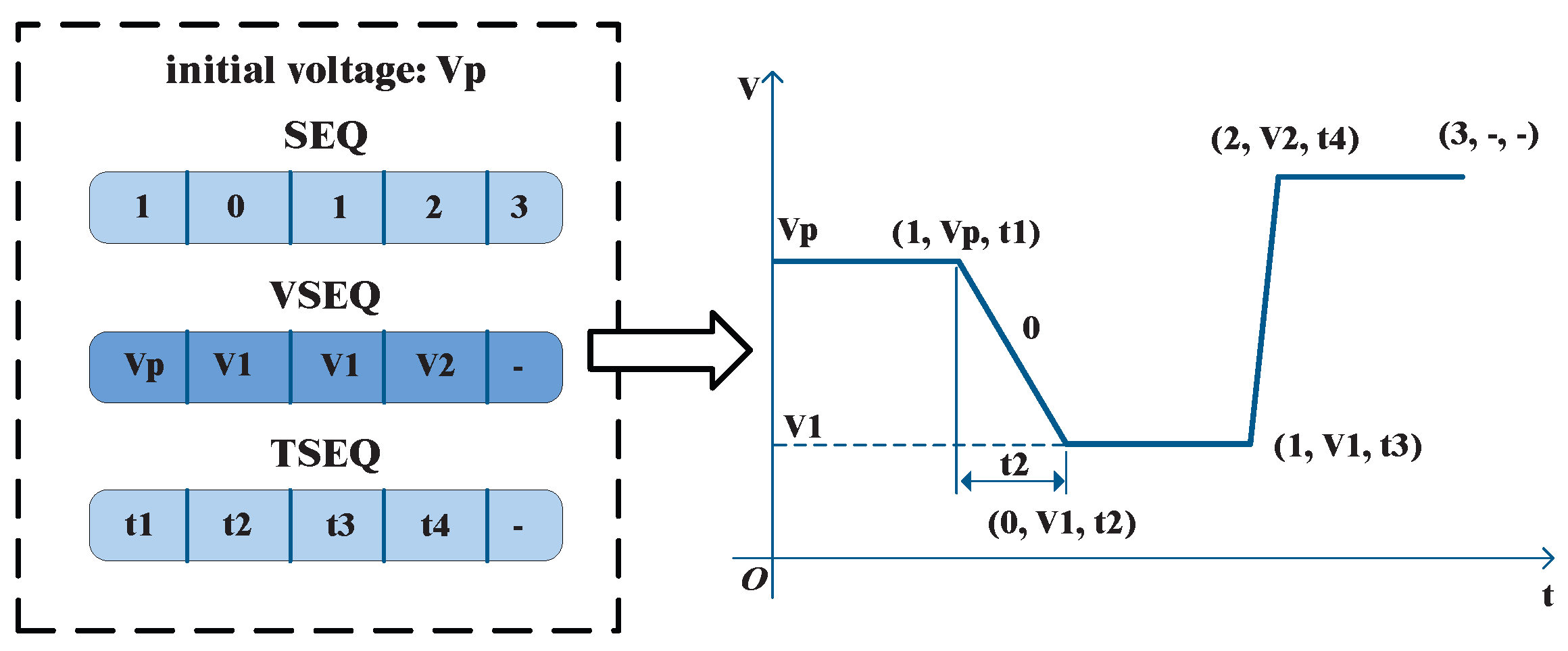
The VGenerator module supports flexible configuration of drive waveforms, implemented based on a three-array waveform description method, as shown in
Figure 6. The SEQ array is used to define waveform types (0 represents a falling edge, 1 represents a horizontal segment, 2 represents a rising edge, and 3 signifies the end of the waveform). VSEQ is the voltage array, where each value indicates the next voltage value for the current waveform segment (falling/rising/horizontal) to be generated. TSEQ is the time array, specifying the duration of each waveform segment. Vp represents the initial voltage, from which all waveforms begin generating. The waveform data are provided by the user and loaded from memory through the accessMem module for use by the VGenerator. This three-array-based structural design not only makes the waveform generation process efficient and easy to manage but also allows for flexible handling of various types of drive waveforms. Consequently, it meets the requirements of diverse application scenarios by accommodating a wide range of drive waveform configurations.
The VGenerator module generates some types of drive waveform that include preheating waveforms, small ink droplet waveforms, medium ink droplet waveforms, and large ink droplet waveforms. Before the start of printing for each column, a preheating waveform must be generated once. To distinguish the type of waveform currently required, we use an array M to record the sequence of waveform types that need to be generated. The values 1, 2, and 3 in the M array represent small, medium, and large ink droplet waveforms, respectively. This ensures that the system can accurately select and generate the corresponding waveforms based on specific requirements.
The VGenerator module cannot directly output the analog vcom waveform; a DAC chip is required to convert the digital signals generated by this module into the vcom waveform. The signals required by the MAX5183 DAC chip are shown in
Table 2.
In this module, the DACEN is set to 1 and PD is set to 0, placing the DAC chip into wakeup mode. The CSn signal is set to 0 to select the DAC chip. The CLK signal is a 10 MHz clock generated by the PLL. The shape of the vcom waveform is determined by the D9–D0 data, which are calculated for the falling and rising edges of the D9–D0 data using the following formulas: (
2) is used for the falling edge and (
3) is used for the rising edge:
In the formulas, D90 represents D9–D0. denotes the voltage value at the next point, which is obtained from VSEQ. is the current voltage value, corresponding to the value of the previous point. signifies the duration of the falling edge, rising edge, or horizontal segment of the waveform, as obtained from TSEQ. represents the number of clock cycles elapsed since the current point, starting from 0 and continuously incrementing up to .
The VGenerator module must complete the generation of a preheating waveform, small ink droplet waveform, medium ink droplet waveform, or large ink droplet waveform within the waiting time of the MGenerator. Afterwards, it waits for the MGenerator’s next latch signal to finish before starting to generate a new drive waveform.
3.4. accessMem Module
The waveform generation system achieves rapid switching of drive waveforms through the accessMem module. The data required for waveform generation are meticulously organized and stored in memory, encompassing SD, MD, preheating waveforms, small, medium, and large ink droplet waveforms, the M array, and the initial voltage Vp, as detailed in
Figure 7. To optimize management and access efficiency, the data are grouped by nozzle columns and arranged sequentially according to the printing order. Within each group, the data adhere to a specific ordering: first, the SD and MD data, followed by the preheating waveform, small, medium, and large ink droplet waveforms, the M array, and finally, the initial voltage Vp. The waveform data are stored in the sequence of the waveform array (SEQ), voltage array (VSEQ), and time array (TSEQ), ensuring that all parameters related to a particular column’s printing are closely associated. This structured and orderly data organization not only guarantees that all necessary parameters can be swiftly retrieved when generating waveforms for a specific nozzle column—thereby accelerating access speed and enhancing waveform generation efficiency—but also ensures smooth waveform switching during the actual printing process by storing the data in the order of the printing sequence. This smooth switching is crucial for achieving high-quality printing. Furthermore, this data layout simplifies the management and maintenance of waveform data, enhances the overall performance of the system, and makes it more efficient and flexible to meet diverse application requirements.
To accelerate the data retrieval process from memory, we set the memory clock frequency to 50 MHz. The accessMem module reads data from memory via the AXI bus and initially stores it in BRAM. Once the reading is complete, the data are sequentially read from BRAM and distributed to other modules for use. Specifically, the clock frequency for writing data into BRAM is also set to 50 MHz to ensure consistency and efficiency in memory interactions. Conversely, the clock frequency for reading data from BRAM is set to 30 MHz, aligning it with the clock frequencies of the SGenerator and MGenerator modules. This alignment avoids issues related to cross-clock domain data transmission, thereby ensuring the system’s stability and reliability.
All data are processed by the ARM core to handle the image to be printed and to determine the drive waveform shape for each position before being stored in memory. This means that, when the data are stored in memory, the different types of drive waveforms for each nozzle position (such as preheating waveforms, small ink droplet waveforms, medium ink droplet waveforms, and large ink droplet waveforms) are already fixed. Due to the grouped storage method employed, a complete group of data must be read from BRAM before printing each column. Each group of data includes information for the preheating waveform as well as the small, medium, and large ink droplet waveforms. Consequently, during the printing of different columns, preheating and ink droplets of varying sizes can utilize different waveform configurations. The waveform-switching time depends on the time required to read one column’s data from BRAM.
Except for the initial BRAM read, each subsequent data read from BRAM is triggered when the MGenerator module generates the ninth ML_n signal. Therefore, it is crucial to ensure that the time required to read a group of data from BRAM is less than the combined time taken to generate the preceding eight waveforms, thereby remaining within the waiting time of the SGenerator module. This timing arrangement guarantees that the data retrieval process does not interfere with the continuity of waveform generation and enables the entire system to operate efficiently within stringent time windows. Consequently, this maintains the smoothness and precision of the printing operation.
3.5. Device Register and Driver
The Registers module is used to store the state of the waveform generation system and to communicate with the software running on the ARM core. The module contains a 32-bit register, with the upper 8 bits designated as the Rstart flag, the middle 8 bits as the Rend flag, and the lower 16 bits as the Length parameter. When Rstart is set to 1, it indicates that the system has begun generating waveforms; when Rend is set to 1, it signifies that the system has completed waveform generation. The Length parameter is used to specify the amount of data that the ARM core writes to memory. This register is mapped to the physical address 0x40000000 and is accessed via the AXI bus.
Communication between the ARM core and the Registers module requires corresponding driver support. In designing this driver, we first use the ioremap function to map the physical address 0x40000000 to the virtual address space, thereby obtaining the corresponding virtual address. Subsequently, the readl and writel functions are employed to perform read and write operations on the register, enabling efficient communication between the ARM core and the Registers module.
4. Experiments
The experimental setup of this study comprises both hardware and software environments. The hardware environment includes a ZYNQ-7020 development board, a MAX5183 DAC chip, and an oscilloscope. The software environment consists of vivado 2023.1 and petalinux 2018. After completing the hardware design using vivado, a bitstream file is generated and programmed onto the development board to configure the hardware. Subsequently, petalinux is utilized to build the device tree, Linux kernel, root filesystem, and uboot bootloader. These components are then placed on the SD card accompanying the development board to boot the Linux system. Within the Linux system, pre-designed driver programs and a client application are executed, with the client application responsible for writing waveform description data to memory. Upon initiating the waveform generation process, the DAC chip converts the digital waveform data into analog signals, which are subsequently input into the oscilloscope for observation.
4.1. Functional Test
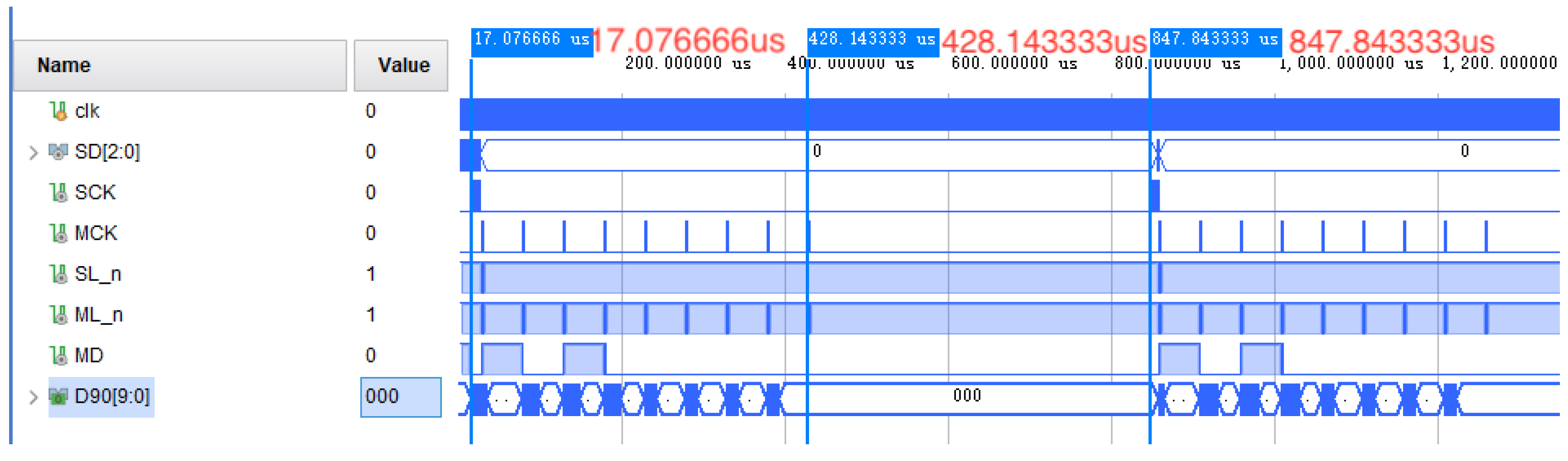
First, we verified the functional correctness of the system through simulation. To comprehensively test the waveform generation system, we developed a simulation program that emulates the memory environment and stores a column of print data into it. The simulation results are shown in
Figure 8. The latch signals SL_n and ML_n are pulled low, following SCK and MCK, respectively. After the SL_n signal is pulled low, nine ML_n signals occur, and both SL_n and ML_n signals wait for a certain period after being pulled low. This behavior is consistent with the designed functionality for generating pixel waveform selection signals and inkjet control signals, thereby verifying the correctness of the system logic.
Next, we verified whether the waveform generation system could achieve flexible waveform configuration. To this end, we developed an application program in the Linux environment to write a group of waveform data to the starting position at memory address 0x38000000, including SD, MD, preheating waveforms, small, medium, and large ink droplet waveforms, the M array, and the initial voltage. For ease of observation and verification, we set all values in the M array to 3, ensuring that the waveform generation system only produces large ink droplet waveforms. Specifically, we configured the large ink droplet waveform as a unipolar M-shaped waveform, with the durations of the rising edge, falling edge, and horizontal segment each set to 2 µs, and the initial voltage set to 0 mV. Subsequently, the driver program wrote 0x01000060 to address 0x40000000 to initiate the waveform generation process. The experimental results are presented in
Figure 9a. As illustrated in the figure, the generated waveform exhibits the expected M shape, with an initial voltage of 0 mV and a falling edge duration approaching 2 µs, which aligns perfectly with the configured parameters.
Subsequently, we configured the large ink droplet waveform to a unipolar W-shape, setting the durations of the rising edge, falling edge, and horizontal segment each to 3 µs, and the initial voltage to 200 mV. Upon initiating the waveform generation, the experimental results are presented in
Figure 9b. As shown in the figure, the generated waveform exhibits the expected W-shape, with the initial voltage accurately reaching 200 mV and the falling edge duration approaching 3 µs, which is entirely consistent with the configured parameters.
Then, we verified the waveform switching between two columns. First, we set the large ink droplet waveform of the first column to an M-shape with an initial voltage of 0 mV. Then, we configured the large ink droplet waveform of the second column to a W-shape, also maintaining an initial voltage of 0 mV, and introduced a single-pulse preheating waveform to ensure a smooth transition from the M-shape to the W-shape waveform. Upon initiating the waveform generation process, the experimental results are presented in
Figure 10. As shown in the figure, the large ink droplet waveform of the first column successfully and smoothly transitioned from the M-shape to the W-shape after the single-pulse preheating stage. This outcome verifies that the system is capable of switching waveforms between columns, achieving the intended waveform transition effect. It ensures printing quality while also demonstrating the system’s flexibility and precise control capabilities.
Our test results demonstrate that the waveform generation system is not only fully functional but also exhibits a high degree of flexibility and precision. The system is capable of finely adjusting the geometric shapes of drive waveforms, the durations of each waveform segment, as well as the voltage values of the rising and falling edges. Additionally, it possesses the ability to smoothly switch waveforms between different printing columns.
4.2. Analysis of Waveform-Switching Time
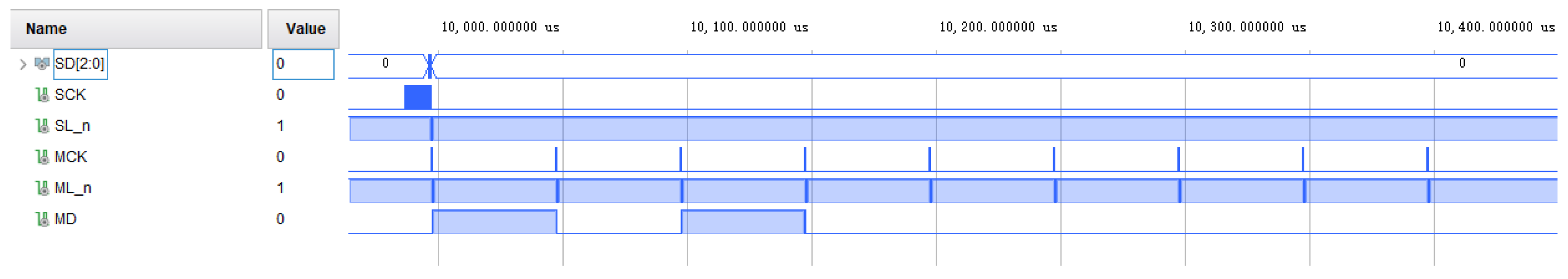
In vivado simulations, the interval time between printing two columns is shown in
Figure 11. According to the simulation results, the interval time between two columns is 830 µs, of which the interval between the generation of the ninth ML_n signal by the MGenerator module and the start of the next column’s printing is 420 µs.
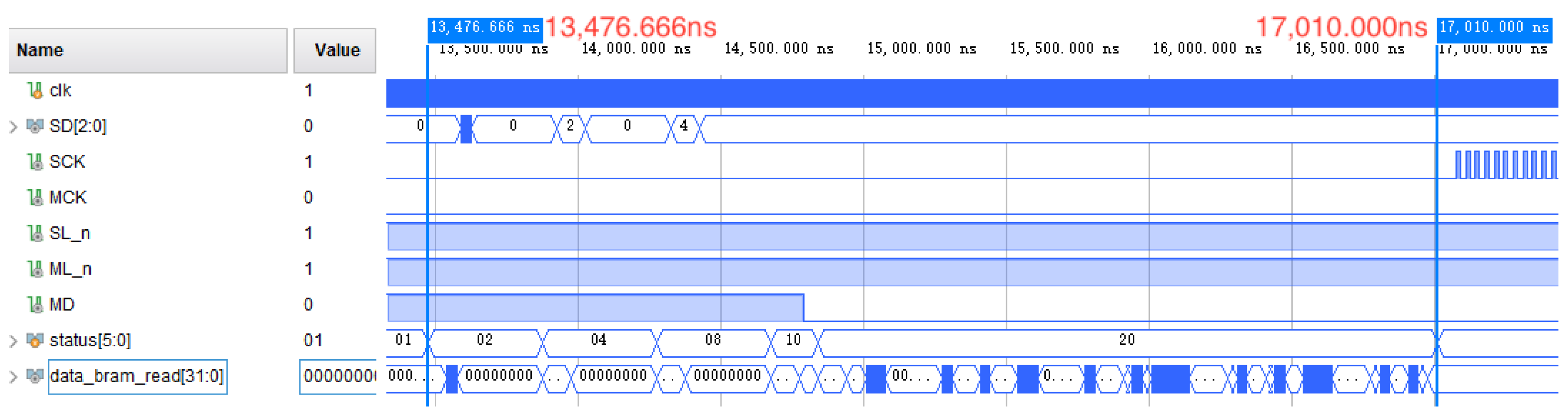
The time required to read a group of data from BRAM is illustrated in
Figure 12. In the figure, status represents the state register of the BRAM read state machine, which starts at 0 and eventually returns to 0, indicating the completion of the data-reading process. As shown in the figure, the time required to read a group of data is only 4 µs. This duration is significantly shorter than the 420 µs interval, ensuring that the data-reading process does not interfere with the initiation of the next column’s printing. Instead, it allows for rapid data loading, adequately preparing for the waveform switching of the next column.
To quantitatively evaluate the efficiency advantage, the proportion of switching time to the total printing cycle can be calculated as follows:
where
is the total interval between two columns and
the waveform-switching time (data loading from BRAM).
To further characterize the system’s high-speed printing capability enabled by the low waveform-switching latency, we estimate the maximum achievable column printing frequency based on the total time interval between two columns. This provides an upper bound for the system throughput under the current configuration.
where
denotes the maximum column printing frequency (in columns per second), and
is the time interval between two printing columns. According to our simulation results in
Figure 11, this interval is measured as
. Substituting into Equation (
6) gives
It is worth noting that the above throughput is not the theoretical upper limit of the system. Since the waiting times of the SGenerator and MGenerator modules are configurable, the total column interval can be further reduced through careful timing optimization. Specifically, by ensuring that the interval between the generation of the ninth ML_n signal by the MGenerator module and the start of the next column’s printing is no less than 4 µs, normal waveform switching and stable system operation can be guaranteed. This flexibility not only enhances printing efficiency but also ensures the accuracy and reliability of waveform switching during high-speed printing processes. By finely adjusting the waiting times, the system is able to implement a more compact time schedule without compromising print quality, thereby improving overall performance.
5. Conclusions
This paper addresses the challenge of waveform dynamic adaptability in industrial piezoelectric inkjet systems under heterogeneous material printing scenarios. Unlike commercial printhead controllers that require printing interruption or parameter reloading for waveform updates, we propose and implement a real-time switching-capable FPGA-based waveform generation system. The key innovations include the following:
Continuous printing compatibility: Dynamic waveform switching within 4 µs during column-wise printing through structured BRAM read mechanisms;
Unprecedented adaptability: Real-time waveform adjustment for heterogeneous surfaces without process interruption, a capability unreported in existing commercial systems;
Design extensibility: Modular FPGA architecture enabling easy reconfiguration of pixel waveform selection and inkjet control signals.
The three-array parameterization method provides granular control over waveform geometry, segment duration, and edge voltages, while the register configuration and peripheral expansion designs offer practical references for industrial implementations. This work bridges a critical gap in dynamic multi-material printing, where traditional systems’ interruption-based switching fundamentally limits application scenarios. Experimental results confirm the system’s 4 µs scale switching latency and continuous printing stability, demonstrating direct commercial translation potential for high-mix production environments.
While the proposed system supports per-nozzle waveform control through a flexible array-based description mechanism, its scalability is currently limited by the fixed size of waveform storage arrays. In future work, we aim to explore more efficient waveform storage strategies, such as waveform compression, parametric generation, or template-based encoding, to enable real-time control of larger nozzle arrays without excessive memory overhead.
Additionally, we plan to investigate scalable architectural designs that can support industrial-scale printheads with thousands of nozzles, and incorporate adaptive waveform selection algorithms based on image content or substrate properties to further enhance printing quality and efficiency. These directions will help evolve the system into a more intelligent and scalable platform for next-generation industrial inkjet printing.


