1. Introduction
Basic arithmetic functions are the basis for complex computational systems such as addition, subtraction, and multiplication that are required within a fast Fourier transform [
1] or addition operations needed within a multiplier [
2]. The development of these basic arithmetic functions (addition, subtraction, multiplication, division) becomes non-trivial when creating the operations within a circuit environment, especially as technology continually progresses to higher operating speeds while striving to decrease power consumption. With the further development of 5G/6G technologies, these basic arithmetic operations require the additional capability of maintaining signal integrity while introducing as little noise as possible for small input signals. Therefore, it can be challenging to design and implement a low-power, high-speed arithmetic function while simultaneously considering how much noise is generated within the circuit topology.
A typical implementation of an adder circuit topology is within Field Programmable Gate Arrays (FPGAs) utilizing fully digital constructs [
3]. However, FPGA implementation can be extremely power-intensive while also over-utilizing resources that may be unnecessary for the arithmetic operation. On the other hand, purely analog adder topologies offer extremely low power consumption at the cost of higher speed operation and slightly more complex circuit architectures to accommodate analog signal pathways [
4]. Additionally, there has been work on creating an adder circuit topology utilizing newly implemented devices [
5]. These newly developed devices are not widely available and would be cost prohibitive to utilize in mass-produced integrated circuit designs.
Mixed-signal design methodologies offer the best approach with low power consumption and high-speed operation with the added bonus of low noise capability [
6]. In [
7], a hybrid analog/mixed-signal adder topology is presented that achieves low delay and low power consumption suitable for a variety of applications. In [
8], another hybrid approach is presented that is capable of achieving adder operation at 8 GHz at a lower supply rail of 0.9 V. Likewise, Refs. [
9,
10] implement mixed-signal adder circuits that demonstrate higher speed operation while maintaining a desired low power consumption. However, all these circuit designs do not consider the impact of noise on their systems as they stick to a purely digital output signal rather than a sine signal that would be seen in communication systems.
Delving deeper into the relevant literature, the adder presented in [
11] is a part of a system that can produce sine wave outputs for a specific modulation pattern. The adder within the given architecture demonstrates a digital methodology using a ripple carry adder topology for the design. The adder functions effectively at 5 GHz, but the overall system design is conducted within a SiGe (Silicon Germanium) technology node, which has improved high-frequency characteristics as compared to standard Silicon CMOS (Complementary Metal-Oxide-Semiconductor) technology nodes. The specialized technology node offers substantial performance metrics for the signal processing time of the adder at higher frequencies. Likewise, the analog adder design presented in [
5] utilizes a specialized Indium–Gallium–Zinc-Oxide think-film transistor technology to produce a low-power system. Like the proposed design, this low-power adder architecture uses only analog signal processing techniques to accept a sine signal at the inputs and output a sine signal as well. While this specialized technology offers significant low-power operation at 78 μW (micro-Watt), the system is not capable of operating above around the 100 kHz range, which significantly hampers its capability for inclusion in high-frequency communication systems.
While many digital systems use FPGA-designed adders, building a custom adder design such as shown in [
8] enables significant customization capabilities like those seen in the proposed design. The presented adder circuit can operate at a maximum frequency of 8 GHz within a 16 nm technology node while detailing improved power consumption results of 1 μW at these high frequencies with a load capacitor of 1 fF (femto-Farad). While this work details a promising full adder circuit design, the adder cannot be utilized directly for the combination of sine signals without additional circuit constructs converting the analog signal into a digital one for standard bit addition. Similarly, the adder topology presented in [
12] details a digital bit adder design in a 45 nm technology node that has low power consumption (in the low nano-Watt range) while operating at a 100 MHz (Mega-Hertz) frequency. Again, the presented design shows significant improvements in transistor count and power consumption but does not offer any capabilities for insertion into a signal processing system that requires analog input/output structures. Therefore, these standard adder design architectures lack the suitability for implementation within a purely analog signal processing architecture that is desirable for high-frequency communication systems.
This paper presents the design of a low-power, high-speed adder circuit topology that utilizes current-starved inverters to decrease power consumption while maintaining a low input-referred noise suitable for communication systems. Current-starved inverters offer unique benefits over the previously discussed systems. Their circuit structure and design provide the capability for the end-user to control the amount of power consumption within the system while simultaneously being easy to utilize and integrate into signal processing systems since they are inherently digital constructs (inverter base structure) that many designers already have a high familiarity with these circuits. These advantages coupled with the fact that they do not require specialized processes outside of CMOS structures to be implemented lead to their advantages over other signal processing constructs that may be included within a system. The proposed design addresses the gaps of analog/mixed-signal design in high-frequency communications systems for high-speed and low-noise application environments by detailing a small and robust circuit design that can be easily recreated for inclusion into larger systems without requiring excessive power or adding much noise to the signal pathways. The paper is organized as follows:
Section 2.1 details the adder structure and basic operation;
Section 2.2 describes the circuit implementation of the adder architecture;
Section 3 shows the experimental simulation results obtained within the 22 nm FDSOI technology;
Section 4 delves deeper into the results with a comparison to other instances of the literature; and
Section 5 summarizes the results and discusses any future work.
3. Results
The current-starved circuit topology was implemented within the 22 nm FDSOI (Fully-Depleted Silicon-on-Insulator) technology and within the Cadence Virtuoso design suite using transistor models provided by the commercially available integrated circuit foundry. The transistor models provide simulation characteristics across process, voltage, temperature, and frequency to account for the functional variability that the transistor devices exhibit due to varying design parameters. The commercially available models combined with the Cadence Design Suite offer extensive simulation capabilities that detail the capacitive and inductive characteristics of the transistors up to the transition frequency of the devices via detailed transfer functions that are provided by the foundry to the university. Therefore, any variance in capacitance or inductance is already taken into account by the Cadence simulator. The Cadence Design Suite was utilized as it is the leading integrated circuit design software for both industry and academia and has extensive useful software modules that generate meaningful integrated circuit design results through a variety of simulators. The Analog Design Environment spectre simulator used in these circuit designs offers a variety of functionalities from transient simulations to noise analysis that lead to a more detailed characterization of the design.
The power supply was set to be 0.8 V with the “” and “” signals being set to 10 nA and 100 nA, respectively. A third condition was used to determine the power and noise parameters for the circuit via a 5 GHz signal passing through the adder with either in-phase signals, signals 90° out of sync, and signals 180° out of sync. All results in the figures are taken from the Cadence Virtuoso design simulator for further analysis. Additionally, the output differential signal in each figure is attenuated as compared to the input differential signals due to current-starved inverters’ gain response at high frequencies. The sine signal was chosen to determine the best response for the adder topology if it was inserted into a telecommunications system where sine waves comprise the input and output signals from and to antennas, respectively. The goal of only utilizing the sine wave is to show the circuit performance characteristics if analog signal processing was undertaken rather than the normally power and time intensive digital conversion and analysis. The utilization of the sine wave is to input signal types that would be highly present in communications systems. The sine wave is the base structure that most communication systems use to modulate important information with varying higher frequency sine signals based upon the type of communication protocol. Showing the results with sine waves demonstrates the proposed design’s capability to be effectively inserted into a signal processing system for communication applications.
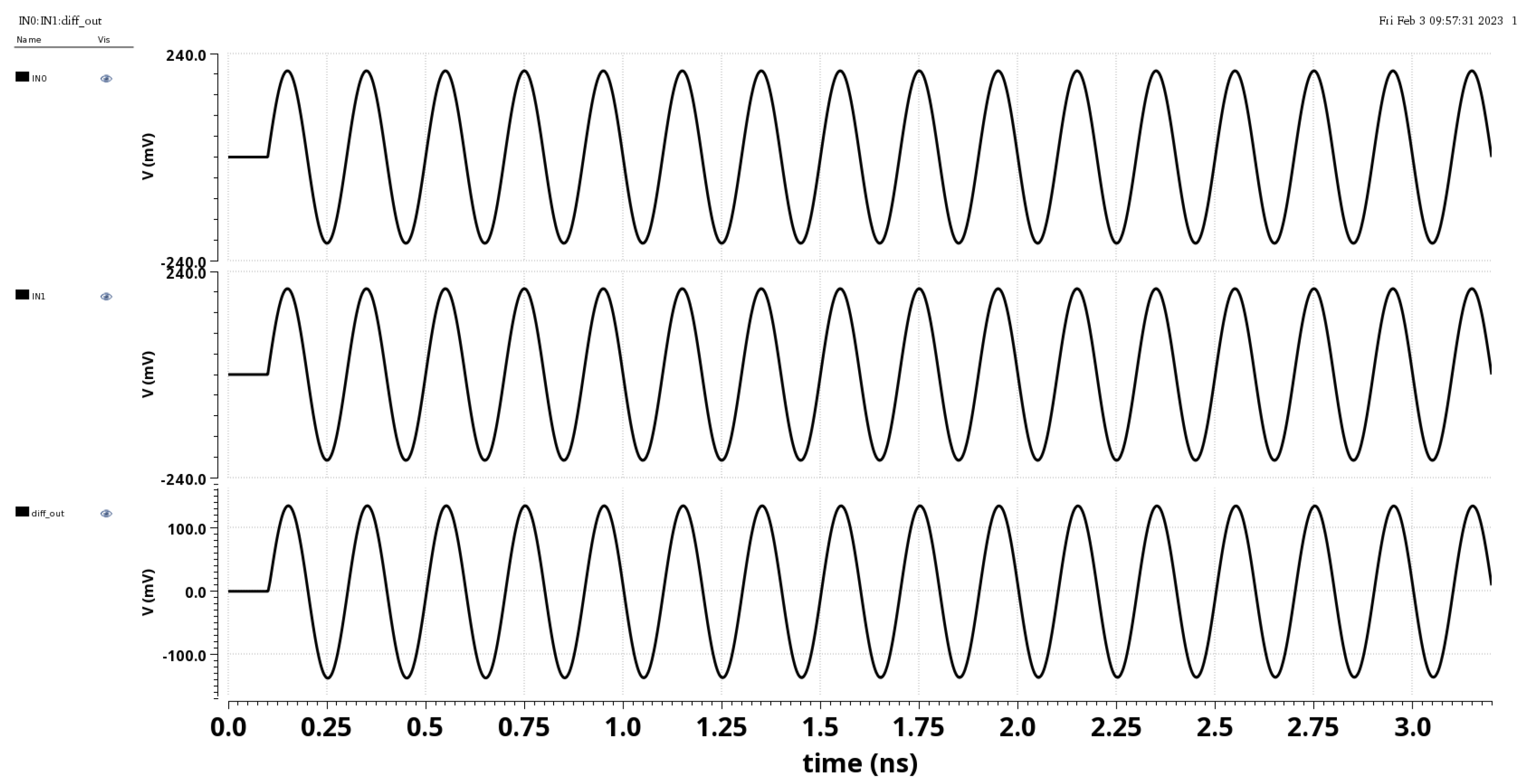
Figure 4 details the two differential input signals (top two signals) with the differential output signal (bottom signal) while the two input signals are in-phase with each other. The current draw for this experiment is 184.6 nA leading to a power consumption of 147.7 nW. The output differential signal experiences attenuation from the current-starved inverters and system design with an attenuation value of 4.082 dB. The in-phase experimental results are the least strenuous on the circuit and result in lower current and power consumption for the design.
Figure 5 depicts the two differential input signals (top two signals) with the differential output signal (bottom signal) while the two input signals are 90° out of phase with each other. The current draw for this experiment is 187.2 nA leading to a power consumption of 149.8 nW. Again, the output differential experiences an attenuation of 6.02 dB due to the circuit design and structure. The 90° out of phase test results are the middle ground experiment for the adder circuit topology and represent a more common current draw and power consumption that would be seen in a typical system operation with this circuit.
Figure 6 shows the two differential input signals (top two signals) with the differential output signal (bottom signal) while the two input signals are 180° out of phase with each other. The current draw for this experiment is 190.5 nA, leading to a power consumption of 152.4 nW. The output differential signal shows full attenuation due to the two signals canceling each other out completely. The 180° out of phase experimental results are the most strenuous on the circuit and result in the highest current and power consumption for the design as the differential signals are constantly on within the circuit and canceling each other out at the outputs of the adder. The three results detail how the current-starved inverter structure operates effectively given various input signal conditions while maintaining a design with low-power, low-noise, and high-frequency operation. Additionally, it is highly pertinent that the signal integrity of the input signal be maintained such that no degradation (noise) is introduced by the design, which can be seen in the clean output sine signal obtained in the above figures. Practically, these results line up with current applications in real-world systems as to what one would expect from the different phase alignments. Also, the low-power and low-noise results would align well with what system designers would aim for within practical communications systems for a circuit that adds two sine waves. The minimal noise insertion while maintaining low-power operation are key benefits to any communication systems within the ever-growing application space.
4. Discussion
Utilizing the results from
Section 3, the input-referred noise for the adder circuit for all three experiments is 6.091 nV/
. This noise level extrapolates to a noise floor for the circuit at or above 0.4307 mV amplitude for the input signal prior to noise washing out the signal pathways. The noise results are obtained from the same simulator as the transient signals but do not produce any graphical results besides the input-referred noise number. The noise level depends solely on the number of transistors in the design and their connectivity rather than signal propagating throughout the design, which can be seen in all three signals having the same noise level. The results for all three experiments are summarized in
Table 1 below. The major limitation and drawback of the proposed adder topology is the attenuation of the current-starved inverters at higher frequencies. This limitation can be countered by increasing the current draw and thus by the power consumption reducing the novelty of the design, as well as by analog/mixed-signal implementation. Additionally, changing the biasing settings for the simulations from the provided numbers in
Section 1 would only change the amplitude of the sine signals via varying the gain of the core inverter transistors as well as either speeding up or slowing down the edge transitions depending on whether the current is raised or lowered, respectively. The noise levels would also change based upon the varying gain due to the gain’s effect on the inverter core’s transistor functionality.
Table 2 compares the results of this work with adder topologies that are close in structure to this design. The comparisons are skewed since standard adder designs are created for digital systems and very little work was found for analog/mixed-signal adders for communications applications. The proposed design shows significant improvement in frequency, although it is in the middle in terms of power consumption and largest for transistor count (single-sided only) for reported values.
Table 2 shows the middle ground simulation results from the proposed adder with 90° out of phase signals to the best results from the compared works. The proposed adder topology significantly outperforms its counterparts via increased frequency with similar or less power consumption (even though typical circuit operation at higher frequencies requires higher power). Additionally, the proposed design achieves this novelty with a higher transistor count as well as decreasing noise contributions to the high-frequency signal pathway. The main exception is from [
12], which shows a markedly improved power consumption, but the design utilizes only 100 MHz signals and remains in the digital domain as compared to the proposed adder’s design for analog communication systems. While the digital designs may not have accounted explicitly for noise contributions due to utilizing digital signaling, analog signal processing requires limited noise contributions to maintain signal integrity during the processing tasks (such as addition). Using the transistor count metric instead of area is meant to detail the relative size of each circuit design through the varying technology nodes as direct comparison would result in smaller technology nodes appearing better than larger nodes. The main aspect is to show that while the technology node for the proposed design is smaller than all but one compared design, the work shows higher frequency operation at a low power consumption. Noise comparison is not considered within this table since not every circuit was explicitly designed for this criterion. The idea to design a circuit with lower noise contributions is extremely beneficial to analog/mixed-signal communication systems and their designs. Therefore, the proposed work focused on achieving good signal integrity, lower power consumption, and improved noise contributions to an analog signal pathway.
While the proposed design is effective at low-noise and low-power operation at the higher frequency domain, the main drawback is the attenuation that occurs within the current-starved inverters. To combat this effect, some design considerations that could be changed would include larger transistor devices throughout the circuit. Larger device sizing would have an impact on the power consumption of the circuit but would offer increased gain attributes and potentially equal or smaller noise contributions depending on which devices are changed. Additionally, different combinations of the current-starved inverters instead of the configuration shown in
Figure 1 could increase the gain of the overall design while maintaining the low-power and low-noise operations.
Within communication systems, low-noise attributes are highly desirable and useful for maintaining signal integrity and propagation. At higher frequencies, the modulation amplitude and signal amplitude will be increasingly affected by small perturbations that noise injection might cause within a given system. This effect is especially true within lower SNR (signal-to-noise ratio) systems where the gain is slight, leading to smaller signal amplitudes overall. Outside of the realm of communications, the proposed design has the capability for utilization within any signal processing system that requires adder circuitry as well as low-noise and low-power operation such as standalone IoT (Internet-of-Things) or implantable biomedical devices that require simple pre-processing of sensor information. The circuit’s suitability for these diverse applications increases its likelihood for inclusion in future wireless signal processing systems.
5. Conclusions
A low-power, high-speed adder circuit topology is presented that utilizes current-starved inverters to demonstrate an addition operation for 5 GHz sine signals for communications applications. The proposed design consumes approximately 150 nW of power with a supply voltage of 0.8 V within a 22 nm FDSOI technology node in addition to outperforming comparable works frequency and power metrics, which are highly useful in communications applications. As discussed in previous sections, the adder circuit topology targets telecommunication systems that aim to remove power- and time-intensive data conversion circuitry by focusing on purely analog signal processing techniques. This implementation requires utilizing sine signals at both the input and output terminals to avoid any digital constructs. Since the adder is focused on analog processing from potential communications antennas, it primarily centers around reducing any noise contribution the design would add, as well as maintaining a low power consumption to keep the overall communication system available power for information transmission rather than signal processing. With the majority of signal processing techniques using digital constructs, the proposed work details the continued importance of how utilizing analog design techniques will achieve similar or better operating conditions than digital counterparts (power, noise, speed) within what is primarily seen as a digital application (wireless signal processing). Future work includes optimization of the adder topology to further decrease power consumption while also pushing for higher frequencies with a lower number of transistors. The proposed adder design is slated for a future tapeout this year to compare measured experimental results to the presented simulated results. Additionally, the development of a current-starved multiplier with the adder topology as its core is in process. These planned future activities will offer the ability to validate the proposed design through experimental verification from fabricated microchips and further utilization of the current-starved inverter core within other signal processing circuitry.


