1. Introduction
High-voltage capacitors are typically used in AC circuits, and measuring them under AC conditions provides a more accurate representation of their behavior under AC operating conditions. The capacitance value can change with voltage and frequency, and measuring them at the specific frequencies and voltages at which the capacitor will be used ensures that the measured capacitance value is accurate for that application. In fact, the impedance of a capacitor varies with frequency and voltage. AC measurements allow for the assessment of dielectric losses, which are frequency-dependent, and these losses can affect the efficiency and the thermal performance of a capacitor.
High-voltage AC capacitance bridges are precision instruments used to measure the characteristics of capacitors, typically the capacitance and dissipation factor (DF). These bridges are crucial for ensuring the accuracy and reliability of measurements in electrical power systems, capacitor manufacturing, and various other industrial applications. The calibration of these devices is essential to maintain their precision and ensure the validity of the measurements they provide for specific voltages and frequencies. Calibration involves comparing the measurements from the high-voltage capacitance bridge to those from a reference standard with known accuracy. This process helps identify any deviations in the bridge’s readings, allowing for adjustments or corrections to be made. Regular calibration ensures that the bridge maintains its accuracy over time, which is vital for ensuring capacitors and other components meet specified standards, monitoring the condition of electrical insulation in high-voltage equipment to prevent failures, and providing precise measurements that are needed when developing new electrical materials and components.
Various types of high-voltage capacitance bridges are commonly used, each operating on different principles, such as transformer ratio arm bridges [
1], Schering bridges [
2], which is an evolution of the Wheatstone bridge principle for capacitance measurements, direct bridge [
3], and the digital bridge principles [
4]. These devices are capable of measuring capacitors ranging from a few picofarads (pF) to hundreds of microfarads (µF) and can handle currents from 10 microamperes (µA) to approximately 10 amperes (A), with larger currents achievable using current extenders like step-down current transformers. The accuracy achieved by these capacitance bridges is typically better than 10 parts per million (ppm) for capacitance and better than 1 × 10
−5 for the DF.
Calibrating and assessing capacitance bridges present challenges due to their high accuracy and the wide range of currents and DFs they can handle. Low-voltage methods are often employed [
5], typically involving comparison to a high-accuracy inductive divider or by comparing two low-voltage capacitors. However, these methods cannot achieve the high currents utilized in calibrations where the bridge compares currents up to several amperes.
High-voltage methods are also used, with the most common method involving the comparison of two reference high-voltage capacitors to calibrate capacitance, while DFs are calibrated by connecting reference resistors in series with the capacitors [
6]. This approach requires a significant number of capacitors and series resistors to cover the entire domain of the capacitance bridges. However, this method poses several challenges, including the need for high-voltage power sources to energize large capacitors, the difficulty in achieving accurate calibration uncertainty for large capacitors, and the requirement for substantial high-accuracy series resistors to cover a wide range of DFs. Overall, whether at low voltage or high voltage, it is challenging to fully cover the entire bridge domain, often resulting in incomplete calibration.
Other techniques utilizing two-phase and amplitude-adjustable current sources have been explored [
7,
8]. In these methods, calibration for capacitance is achieved by introducing known currents into the branches of the bridge, while DFs are determined by controlling the phase difference between the currents. One advantage of these techniques is that calibration is carried out at low voltage, eliminating the need for high-voltage capacitors and power sources. However, achieving a low level of uncertainty requires high-accuracy current-to-voltage converters and a precision voltage and phase measuring system.
Recognizing the potential benefits, we have embarked on developing such a method to improve the calibration uncertainty of high-voltage capacitors by enhancing the accuracy of the capacitance bridge. The goal is to achieve low uncertainties that are applicable across a wide range of capacitances and DFs. This paper primarily focuses on the calibration of the capacitance bridge, structured into three sections: the first section discusses the measurement method, the second addresses uncertainty calculation, and the third presents the calibration results of LNE’s capacitance bridge used for the routine calibration of high-voltage capacitors.
The connection between current and capacitance measurements lies in the fundamental relationship between capacitance, current, and voltage in an AC circuit. By understanding this relationship, we can accurately measure capacitance by observing how current flows through a capacitor when an AC voltage is applied. In an AC circuit, a capacitor’s behavior is described by the fundamental equation , where I(t) is the current through the capacitor as a function of time, C is the capacitance, V(t) is the voltage across the capacitor as a function of time, and dV/dt is the time derivative of the voltage, indicating how rapidly the voltage changes. This equation states that the current flowing through the capacitor is directly proportional to the rate of change in the voltage across it. This relationship is key to measuring capacitance by analyzing the current. When an AC voltage of V(t) = V sin(ωt) is applied to the capacitor, the resulting current I(t) is expressed as .
In a purely capacitive component, the current leads the voltage by exactly 90°. However, in practice, no physical capacitor is ideal. Resistive elements in the insulation material make the capacitor imperfect, ignoring the inductance of the leads. The DF, also known as tangent δ, can be introduced in the complex plane as the tangent between the resistive current and the capacitive current flowing through the capacitor. A significant resistive component indicates that the capacitor has very low dissipation factors. The DF of a capacitor measures the efficiency with which a capacitor stores and releases energy, quantifying the amount of energy lost as heat due to internal losses within the capacitor. This factor is particularly important in applications where capacitors are used for power factor correction and filtering and in circuits that require stable and efficient energy storage. To calibrate a capacitor by comparing it with another under the same voltage (parallel connection) and frequency conditions, the process involves evaluating the ratio of the currents, which is proportional to the ratio of the capacitances, and the phase difference between the two currents. The comparison of capacitance between the two capacitors relies solely on analyzing the complex currents as they provide a direct measure of the respective capacitance values. This is why calibrating the bridge at low voltage by analyzing the complex currents is a powerful method to calibrate the bridge across its entire operational range of voltage and frequency.
2. Materials and Methods
2.1. Principle
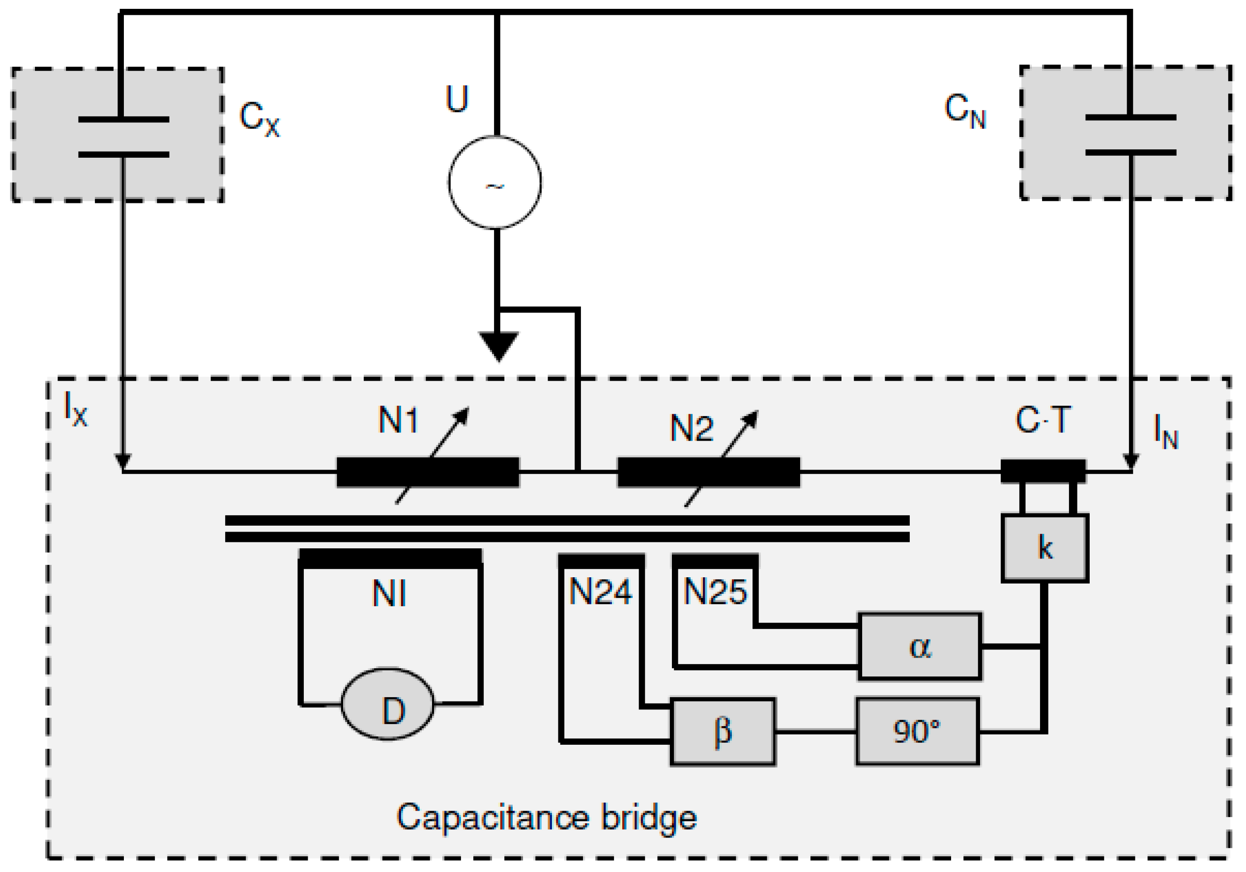
The calibration of a high-voltage capacitor involves using a reference capacitor and a capacitance bridge. Here is how it works: a high voltage, typically ranging from 1000 V to 1 MV, is applied simultaneously to both the reference capacitor and the capacitor being tested. Regardless of the bridge used [
1,
2,
3,
4], the principle remains the same: the bridge analyzes the complex currents passing through both capacitors to determine their capacitance and DF values. Essentially, the capacitance bridge functions as a current comparator. Calibration can be conducted by applying known complex currents to its branches, eliminating the need for high-voltage capacitors, high-voltage sources, or reference DFs. To simulate capacitance, the amplitudes of the currents are adjusted, while the phase between the currents is adjusted to simulate the DF. In
Figure 1, we illustrate the principle applied in this calibration process.
The calibration utilizes two stable sinusoidal alternating current (AC) sources. Specifically, the Type 8100 amplifier from Clark Hess and the Fluke Type 5700A are employed to supply precise current to each branch of the calibration setup. The Model 8100 Transconductance Amplifier is a precision instrument known for its high stability and accuracy. It generates an output current directly proportional to the input voltage over a frequency range from DC to 100 kHz. It features six overlapping ranges, delivering low-distortion output currents from 200 µA to 100 A. The Fluke 5700A calibrator is a high-precision, multifunctional instrument widely used for calibration in various industries and laboratories. It is designed to provide highly accurate voltage, current, and resistance outputs, making it an essential tool for calibrating a wide range of electrical measurement devices, including mustimeters, oscilloscopes, and other test instruments. The Fluke 5700A offers exceptional accuracy, typically within a few parts per million (ppm) for current outputs, delivering low-distortion output currents in the range from 9 µA to 2.2 A. This high level of precision is critical for ensuring the reliability of calibration processes. The high stability of both frequency and voltage is crucial for meeting stringent requirements. Fluctuations in amplitude can impact capacitance measurements, while variations in frequency can affect measurements of the dissipation factor, which is highly sensitive to frequency changes.
The Phase Generator Type 5500, also known as the Clarke-Hess Model 5500 Phase Standard, is an advanced instrument designed to generate precise phase angles between two AC signals. It is widely used in calibration and measurement systems where accurate phase control is essential. The device is particularly useful in applications involving impedance measurements, power system testing, and the calibration of phase-sensitive instruments. It offers exceptionally precise phase control, typically to within 1 m°. It is designed for stability and repeatability, ensuring consistent phase output over long periods and under varying environmental conditions. The phase generator is utilized mainly to generate a fixed phase shift between both current sources. The phase generator is used to precisely set the phase difference between the two current sources. The generator provides fine phase adjustments with a minimum adjustable step of 1 m°. This corresponds to an extremely precise DF adjustment step of 1.7 × 10⁻⁵, allowing for highly accurate control of the phase relationship between the currents.
2.2. Standard Resistors
Two reference resistors, RN and RX, are used to measure the currents. The voltage across the resistors is measured using two analog-to-digital converters (ADCs). The values of the resistors are deliberately kept below 10 kΩ to minimize the influence of stray impedances.
Each resistor’s complex impedance
Z, defined in a 5-terminal configuration, is known through primary calibration [
9,
10], with
Z =
Rdc × (1 +
∆S +
j·ω·τ), where
Rdc represents the resistance value at direct current,
∆S is the relative variation of resistance with frequency, and
τ is its time constant. All resistors used in this procedure have a temperature coefficient better than 5 ppm/°C. To mitigate the temperature effects, the resistors are measured in a regulated chamber at (23 ± 0.2) °C just before and after the bridge’s calibration. The traceability of standard resistors is ensured, firstly, by the calibration of a 1 kΩ resistor by comparison to a calculable resistor up to 1 kHz. Then, this 1 kΩ resistor is used as a reference element to ensure the traceability of all standard resistors using an automated Wheatstone bridge using a step-up calibration procedure for resistors higher than 1 kΩ and a step-down procedure for resistors lower than 1 kΩ. More information about these resistors is described in [
9,
10].
To calibrate the bridge, capacitance values are assigned by applying an appropriate current using the formula I = V⋅ω⋅C. For instance, to calibrate a capacitance CX = 1000 pF by comparing it to a capacitance of CN = 100 pF under a voltage of 100 kV at 50 Hz, the current would be 31.4 mA in the CX branch and 3.14 mA in the CN branch. These currents must be precisely applied to both inputs using dedicated current generators. When using the Fluke 5700A, the current amplitude is set directly using the dial settings. To achieve the desired DF, the phase references of both generators are adjusted using the Clarke-Hess 5500 phase reference. When employing the Clarke Hess 8100, the amplitude and phase of the transducer are controlled directly by the Clarke Hess 5000.
Once the amplitudes and phase shifts of the currents are applied, the bridge is balanced manually using the bridge decades. The balanced state enables measurements using the amplitude and phase measuring system using the automated software. It is crucial that the amplitudes of the current sources and their phase shifts remain stable enough (low time stability) during the measurement acquisition to achieve high accuracy in the measurements.
The values of capacitance (
CX) and DF are calculated using Equations (1) and (2), respectively, and these quantities are compared with the values displayed on the bridge when it is balanced.
In the equations provided:
represents the voltage ratio measured by the ADCs.
indicates the resistance ratio between the reference resistors.
CN denotes the value assigned on the bridge for the calculation of CX.
Δϕ represents the phase difference measured by the ADCs.
Arg (ZX) and arg (ZN) are the impedance arguments of the impedances ZX and ZN.
2.3. The ADCs
We have chosen the Agilent 3458A model [
11] to sample and digitize the signals. This device, which has proven its worth for nearly 30 years in metrology laboratories, remains a reference, particularly for its remarkable stability and linearity characteristics. Three sampling modes are available: a direct sampling mode without a blocker (
fe ≤ 100 kHz), a direct sampling mode with a blocker (
fe ≤ 50 kHz), and a sequential sampling mode with a blocker (
fe > 50 kHz and
fe < 100 MHz).
For this application, we have chosen the DCV mode without a blocker, which allows for quantification with a very high resolution. Indeed, it allows for signal digitization at a sampling frequency ranging from 0.2 Hz (28-bit resolution) to 100 kHz (16-bit resolution). No sample-and-hold circuit is connected, allowing for the integration time Ta (or analog-to-digital conversion time) to be set from 500 ns to 1 s in 100 ns steps (for comparison, using the sample-and-hold circuit fixes the integration time at 2 ns). This characteristic is used to achieve a greater averaging effect and thus limit the dispersion of measurements. After analog-to-digital conversion, a memory storage time Tm is necessary for formatting and storing the data in memory. The values of Tm limit the integration time Ta for a given sampling frequency fe. Equation (3) presents the relationship between these three quantities.
We have determined the minimum values of Tm based on the sampling period (1/
fe) that allow for error-free sampling by analyzing the data storage format of the ADCs (DIN Format and SIN format). The “DINT” format, which can be used for a sampling period of at least 18 µs, corresponds to 4-byte encoding and allows for the highest resolution. For shorter sampling periods, we use the “SINT” format, which corresponds to 2-byte encoding, permitting shorter memory storage times Tm. We have decided to use Equations (4)–(6) to fix the integration times regarding the sampling frequency and the storage time in order to have a resolution much higher than 18 bits:
2.4. The Algorithm
The choice of the type of digital processing of the samples is, of course, one of the important aspects of the method. Two possibilities were considered:
The first possibility is signal processing via complex Fourier transform and processing via least squares approximation. The complex Fourier transform allows access to the amplitude and phase of the fundamental frequency as well as the amplitude and phase of all the harmonics. Since our measurand is defined for sinusoidal signals, only the information concerning the fundamental frequency is useful to us. In this case, evaluating the amplitude and phase of the signals involves determining the maximum level of the observed line in the magnitude of the Fourier transform and considering the corresponding phase. In practice, since the number of operations that can be performed is not infinite, we must apply a Discrete Fourier Transform algorithm (e.g., the FFT algorithm). In this case, the frequency representation is sampled, and it is necessary to ensure the coincidence between the peak of the spectral line and a sampling point. To achieve this, the sampling frequency must meet Equations (7) and (8).
For a time sample of one period:
For a time sample of
Nper periods:
where
fe is the sampling frequency,
fS is the fundamental frequency of the signal, and
N is an integer ensuring that the maximum of the spectral line coincides with a sampling point.
Therefore, this condition requires control over the ratio between the sampling frequency and the signal frequency. A phase-locked loop (PLL) can be used to ensure this condition.
The second possibility is using the least squares approximation method, which involves modeling a signal by adjusting the parameters of a defined function to minimize the squared differences with the processed sample. By selecting a sinusoidal function, only the fundamental of the signal is processed, and the influence of any harmonics must be considered in estimating the measurement uncertainty. This type of processing, simpler to implement than discrete Fourier transformation and apparently well-suited to our needs, has been chosen. It is advisable to consider extending the measurement range above 1 kHz by configuring the ADC in sequential sub-sampling mode, as conditions (7) and (8) cannot be met otherwise. The least squares approximation is more suitable for any future extension of the measurement up to at least 100 kHz.
A fitting algorithm was then employed to analyze the signals. A sinusoidal function can be described by four parameters: its amplitude
A, frequency
fs, phase
ϕ, and offset
Δ. The Levenberg–Marquardt algorithm is commonly used for non-linear least-squares fitting in such cases. However, like all iterative techniques, it is highly sensitive to the initial parameter values. To mitigate this sensitivity, accurately estimating the initial parameter set is crucial before initiating the optimization process. For initialization, Equations (9)–(12) were utilized.
Equation (9) demonstrates that a sinusoidal function can be represented using a linear system with three parameters. These parameters can be estimated using a linear least-squares fitting algorithm. The advantage of this approach is its non-iterative nature—it simply solves equations—eliminating the need for initial parameters. Additionally, it requires minimal computation time and is unbiased. We opted to utilize a Singular Value Decomposition (SVD) algorithm arbitrarily. This algorithm, operating under the assumption that the frequency
fs is equal to the nominal signal frequency, is executed prior to the non-linear four-parameter fitting algorithm, as illustrated in
Figure 2.
To verify the effectiveness of this chosen combination through numerical simulations, we considered 500 periods of a pure sinusoidal signal sampled at 50 points per period. The algorithm accurately reproduces the values of the sinusoidal signal without error. During measurements, 70 periods and 50 samples acquired per period for each measurement point are considered sufficient. It is worth noting that the resolution of the ADCs was maintained higher than 18 bits, ensuring a very low voltage quantification error. To minimize random errors more effectively, each point was repeated 10 times.
2.5. Measurement of the Phase Difference
In Equation (2), measuring a phase difference
between two sinusoidal signals is equivalent to measuring their time shift
ΔT using Equation (13)
Any element of the device causing a time shift between the signals is, therefore, a source of error in the phase measurement. The sampling of the signals is controlled by an external signal simultaneously on both ADCs. However, it consistently appears that the response time of the samplers differs from one device to another. Thus, this discrepancy is the source of a systematic error in the phase measurement. Measurements conducted by applying the same signal to the inputs ADC (using the developed algorithm) at different frequencies were able to identify this systematic source. The slope obtained via linear regression reveals a shift close to 20 ns between the response times of the two ADCs (the manufacturer specifies a maximum shift of 25 ns). The associated error, reaching 125 µrad for signals with a frequency of 1 kHz, is too high. In addition, since the accuracy and stability of the internal clock differ from one ADC to another, this systematic error constantly changes depending on the influence of temperature. Rather than applying a phase correction, which would increase the uncertainty, we chose to add an extra step to the procedure by performing an additional measurement step after the signals have been permuted using the switching card shown in
Figure 1. By taking the average of the samples obtained with the two ADCs for each signal, this systematic error is drastically reduced. This procedure also eliminates any difference between the integration times of the two ADCs, which, in theory, is responsible for an error in the determination of the phase shift and amplitude. In practice, no significant effect was shown. We have then considered an uncertainty of about 1 ns (k = 1), and the uncertainty of phase shift regarding the frequency is presented in
Table 1.
On the other hand, the level of harmonics in the signals was kept below 0.01%. Since the phase difference was obtained at zero crossing, any distortion in the signals resulted in significant errors in phase measurements due to fitting inaccuracies. Therefore, it was crucial to keep signal distortions as minimal as possible. A distortion level lower than 0.01% reduces the phase error to less than 1 µrad.
2.6. Measurement of the Voltage Ratio
To check the error of the unity voltage ratio
in Equation (1), several measurements were performed at different amplitudes, ranging from 0.1 V to 1 V, and at different integration times, ranging from 10 µs to 400 µs, using different sampling frequencies. The results shown in
Figure 3 show the voltage ratio uncertainty with respect to the voltage and the corresponding integration time. They are about 1 µV/V level for integration times longer than 50 µs, 2 µV/V for
Ta = 30 µs and 3 µV/V for
Ta = 10 µs. The contribution comes especially from the repeatability of the measurement and the observed maximum deviation from the unity ratio.
In theory, the integration time will have a significant error in the measurement of the voltage amplitude because the integrating process will act as a filter for the signal [
12]. A correction factor could be applied to correct the error of this filter, which depends on the frequency of the signal and the rectangular pulse over which the signal is integrated. However, in our case, and according to (1), the integration time error is perfectly canceled by measuring the voltage ratio of two identical signals (unity ratio) and by configuring both ADCs with the same parameters.
Taking into account the results shown in
Figure 3, the calculated integration in Equations (4)–(6), and the sampling frequency (50 times the signals frequency), the uncertainties relative to the voltage ratio measurement, for each frequency, are summarized in
Table 2.
2.7. Analyses of the Stray Impedances
The limited input impedance of the ADCs results in a significant error in the ratio and phase measurement, especially when high-value resistances are connected to their inputs. Their input resistance
Rf has a linear behavior from 50 Hz to 1 kHz, respectively, and from 10 GΩ to 100 MΩ in the considered sampling mode. The input capacitance is nearly identical in the studied frequency range; it is equal to about
Cf = 450 pF. The resulting error in the voltage ratio is given in Equation (14), and the resulting error in phase shift is given in Equation (15).
When RX and the RN are equal, the errors cancel out. However, when they differ, the errors become significantly larger, especially the phase shift at higher frequencies. Higher resistance and stray capacitance result in higher phase errors. To eliminate the influence of stray impedances and to meet the correct metrological definition of resistance in a five-terminal configuration, two guarded buffers with high input impedance were used.
The buffer principle involves an instrumentation amplifier with differential inputs and unity gain, as depicted in
Figure 4. The common-mode impedance of the non-inverting amplifiers
A1 and A2 (impedance between the inverting input and ground), as well as the stray capacitance of coaxial cables, are crucial for achieving high input impedance. The chosen non-inverting amplifier needed an input impedance greater than several hundred MΩ, with a maximum stray capacitance of a few pF.
For the differential amplifier A3, the critical requirement was its tolerance to capacitive loads, which had to be at least higher than 450 pF (the capacitance of one meter of 50 Ω coaxial cable is 100 pF, plus the capacitance of the ADC is 350 pF). Both amplifiers required a closed-loop bandwidth in the range of tens of MHz to minimize phase shift. The phase shift was fine-tuned to zero using additional variable capacitors in the differential amplifier.
Resistors R1 to R4 were selected with a value of (1000.000 ± 0.010) Ω, which strikes a good balance to limit the gain error to a few tens of ppm. Their temperature coefficients were a few mΩ/°C. A one-meter triaxial cable connected to the resistors via guard amplifiers A4 and A5 (type OPA27) eliminates the capacitance effect by driving the inner cable shield to the same voltage as the center conductor. This reduced the cable capacitance effect to less than 1 pF. A buffer amplifier B was used to increase the tolerance to capacitive loads.
The performance of both buffers was evaluated at up to 1 kHz, and the results are summarized in
Table 3. The absolute phase shift between the input and output voltages is less than 1 µrad. The unity gain error (1 −
Vout/
Vin) is around 20 µV/V, which aligns well with the tolerance of resistors R1 to R4.
3. Uncertainty of Measurement
To achieve the best uncertainties in the chosen operating mode, we decided to add additional steps to the calibration procedure.
When the calibration was performed at a unity ratio of RX = RN and VX = VN, the relationship of RX/RN was determined through a second measurement step. In this step, the bridge was disconnected, and the same current was applied to both resistors in series. The common point was set to ground potential using a “Wagner” circuit. The ratio of VX/VN measured during this step directly represents the ratio RX/RN. The tangent difference measured at this stage represents the tangent difference between the two resistors. This second measurement step includes the systematic errors of the entire measuring circuit (ADCS + buffers + resistors). Therefore, it was unnecessary to calibrate the reference resistors separately; the whole system was self-calibrated.
When the calibration was performed with a ratio different from unity RX ≠ RN but still ensuring VX = VN, the currents in both branches were not the same; the resistors were selected to maintain the same voltage across each one. These resistors were calibrated both before and after the measurements. However, we also decided to add a second measurement step here: the buffers were disconnected from the resistors, and one volt was applied to the input of both buffers. This second measurement was preferred to determine the errors of the ADCs and the buffers instead of calibrating them separately.
The uncertainty of the measurement was calculated for ratios of 1, 10, and 100. A ratio of 1 indicates that the currents flowing through both branches are equal, and the resistors used to measure these currents have the same values. A ratio of 10 means that the current in branch X is ten times higher than the current in branch N. To measure a voltage unity ratio, the resistor in branch N is ten times higher than the resistor in branch X. A ratio of 100 means that the current in branch X is one hundred times higher than the current in branch N. To measure a voltage unity ratio, the resistor in branch N is one hundred times higher than the resistor in branch X. The measurement uncertainties were calculated according to the GUM [
13] (Guide to the Expression of Uncertainty in Measurement), and all uncertainties were considered to be uncorrelated.
3.1. Uncertainty of Capacitance
The contributions come from the following:
u1, the repeatability of the measuring system: 10 series were carried out for each point. In all cases, the repeatability of CX was better than 1 µF/F. The repeatability of the measuring system represents the dispersion of the measurement, which can come from various parameters, such as the resolution and linearity of the ADCs, the stability of amplitude and frequency of the current sources, and the influence of small changes in temperature while performing measurements, especially the temperature dependence of resistors, ADCs, and buffers.
u2, the resolution of the bridge is 1 µF/F. The capacitance CN in (1) was taken in such a way that the resolution is at its highest level. The standard uncertainty of the resolution is 0.29 µF/F, which is obtained by dividing 1 µF/F by (2√(3)) by considering a rectangular distribution law.
u3, the uncertainty of measurement of the ratio (
VX/
VN), as explained above in
Table 2, was better than 1 µV/V up to 300 Hz, 2 µV/V up to 500 Hz, and 3 µV/V up to 1 kHz.
u4, the standard uncertainty of the ratio (
RN/
RX); for a unity ratio, it was equal to 1 µΩ/Ω obtained in a second step by measuring the voltage ratio again, as explained above. For a non-unity ratio, each impedance was calibrated before the measurements, and the uncertainty depends on the value of the resistance, as explained in [
9,
10]. Uncertainty
u4 takes into account all uncertainty contributions from resistors, including drift and temperature effects [
10]. This study did not consider the influence of humidity; however, humidity was maintained below 60% throughout the calibration process.
The uncertainties of the measurement of capacitance are summarized in
Table 4, and for currents above 0.1 mA, we obtained an expanded uncertainty U (k = 2) of about 3.5 µF/F for a ratio of 1 and between 6 µF/F to 14 µF/F for ratios of 10 and 100.
For currents below 0.1 mA, the expanded uncertainties were larger. This increased uncertainty is primarily due to the sensitivity of the bridge: achieving self-balancing of the bridge with very high accuracy is challenging at very low currents. Additionally, calibrating the bridge at low currents requires high resistor values (e.g., 10 kΩ for 10 µA), leading to significant parasitic effects. With the common point of the bridge connected to the ground reference of the buffer, even a small common mode voltage can cause high-frequency oscillations and measurement instabilities. To mitigate these oscillations at very low currents, using a resistor of 1 kΩ instead of 10 kΩ is recommended; the voltage across the resistor is 10 mV at I
N = 10 µA. Although ADCs can measure these low levels, the uncertainty increases due to ADC noise when the voltage is lower than 100 mV. Therefore, we decided to limit the minimum current to 0.1 mA. In most cases, HV capacitance bridges are ineffective below 100 µA due to their very low resolution and measurement instabilities. An alternative solution to determine current non-linearity is detailed in reference [
14].
3.2. Uncertainty of Dissipation Factor
The expanded uncertainties for the DF are summarized in
Table 5 for currents above 0.1 mA.
The contributions come from the following:
u1: This relates to the repeatability of the measurements, which is generally less than 1 × 10⁻⁶. The repeatability of the measuring system represents the dispersion of the measurement, which can come from various parameters, such as the resolution and linearity of the ADCs, the stability on amplitude and frequency of the current sources, and the influence of small temperature changes while performing measurements, especially the temperature dependence of resistors, ADCs, and buffers.
u2: This relates to the resolution of the bridge, which depends on the displayed value. It is generally 0.29 × 10⁻⁶ for dissipation factors (DFs) ranging from −0.001 to +0.01 and 2.9 × 10⁻⁶ for DFs ranging from −0.01 to −0.001.
u3: This relates to the standard uncertainty of the tangent measured, as explained in
Table 1.
u4: This relates to the standard uncertainty of the tangent difference between both resistors. For a unity ratio (
RN =
RX), this error could be equal to u3, which is obtained in a second step by measuring the tangent difference again, as explained earlier. For a non-unity ratio, each impedance was calibrated before the measurements, and the uncertainty depends on the value of the resistance, as explained in [
9,
10]. The uncertainty u4 takes into account all uncertainty contributions from resistors, including drift and temperature effects [
10]. This study did not consider the influence of humidity; however, humidity was maintained below 60% throughout the calibration process.
At 50 Hz, the uncertainty primarily depends on the measured DF and the ratio of the bridge. When the DF ranges between −0.001 and +0.01, we obtained the following uncertainties: 2.2 × 10⁻⁶ for ratio 1, 5.3 × 10⁻⁶ for a ratio 10 and about 7 × 10⁻⁶ for ratio 100. When the DF ranges between −0.01 and −0.001, the uncertainties were slightly higher, by a factor lower than two.
At 1 kHz, the uncertainties are in the range of 20 × 10−6 for any ratio and any DF affected, which is mainly due to the uncertainty relating to the time clock of both ADCs.
5. Discussion
The technique developed in this paper has significantly improved the calibration of capacitance and DF at high voltages. Capacitance bridges play a pivotal role in the measuring chain, but they also require a standard capacitor during calibration. Two coaxial cables are essential for connecting the outputs of both capacitors to the inputs of the capacitance bridge. To reduce measurement uncertainty to below 10 ppm for capacitance and below 1 × 10⁻⁵ for DF, enhancing the calibration uncertainty of capacitance bridges is crucial, as other contributions cannot be significantly improved.
Compressed gas capacitors, based on a coaxial cylindrical electrode structure, are commonly used as reference capacitors due to their extremely low voltage dependence in terms of capacitance and DF. Manufacturers have made substantial efforts to improve electrode coaxiality, a determining factor in the voltage dependence of capacitance [
16,
17]. Various techniques, such as direct comparison [
18], voltage transforming [
19], voltage doubling [
20], frequency doubling [
21], simplified tilting [
22], and kinetic methods [
23], can accurately calibrate reference capacitors. The uncertainties of the reference capacitors could be estimated accurately at 2 µF/F for capacitance and 2 × 10
−5 for DF, values that are scientifically difficult to improve further.
The lengths of coaxial cables can influence measurements depending on the capacitance value and the parasitic impedance of the capacitance bridge. Their impact can be mitigated by crossing both capacitors and averaging the results, although correction factors are needed if the capacitors have significantly different values. The influence of coaxial cables is typically determined with an uncertainty better than 0.5 µF/F for capacitance and better than 5 × 10⁻⁷ for DF.
The method presented in this paper allows for the thorough characterization of capacitance bridges, accurately determining correction factors for both DF and capacitance. As a result, the uncertainty when calibrating high-voltage capacitors, including the standard capacitor, coaxial cables, and capacitance bridge, is now lower than the manufacturer’s claims, reaching values as low as 10 ppm for capacitance and 1 × 10⁻⁵ for DF.


