1. Introduction
The rapid advancement of electronic communication technologies, particularly in 5G, the Internet of Things (IoT), and high-performance computing (HPC), has led to increasing concerns regarding EMI [
1,
2,
3]. EMI not only disrupts the normal operation of electronic devices but also poses potential health risks when exposed over extended periods [
4]. Moreover, EMI can cause malfunctions in sensitive electronic equipment, leading to signal interference and reduced reliability [
5,
6,
7]. As a result, the demand for effective EMI shielding technologies has grown significantly, particularly in the next-generation electronics and semiconductor packaging industries, where the performance of EMI shielding materials is directly linked to product reliability [
8,
9,
10,
11,
12,
13]. Metal-based EMI shielding materials, such as copper, silver, and aluminum, are widely used due to their high electrical conductivity and excellent shielding performance [
14,
15,
16]. However, these materials suffer from several limitations, including high density, susceptibility to corrosion, and secondary EMI pollution due to high reflectivity [
17,
18,
19,
20]. Additionally, metal-based shielding materials pose challenges in manufacturing and processing, making them less suitable for emerging applications such as flexible and wearable electronics [
21]. With the increasing trend toward miniaturization and the high integration of electronic devices, the development of alternative EMI shielding materials that can overcome these limitations has become imperative. To address these challenges, polymer-based EMI shielding materials have emerged as promising alternatives [
22,
23,
24]. Polymer composites offer lightweight properties, flexibility, corrosion resistance, and ease of processing. In particular, conductive polymer composites (CPCs) incorporating carbon nanotubes (CNTs), graphene, and metallic nanoparticles exhibit excellent shielding performance via both reflection and absorption mechanisms [
25,
26,
27,
28,
29,
30]. Recent research has focused on optimizing the dispersion of conductive fillers and structural design to maximize EMI shielding efficiency. Several strategies have been explored to enhance the EMI shielding effectiveness of polymer composites [
31]. One approach involves constructing a three-dimensional (3D) conductive network within the polymer matrix, which enhances electron transport paths and increases EMI attenuation [
32]. Additionally, multilayered and porous structures have been investigated to optimize impedance matching, thereby minimizing electromagnetic wave reflection and maximizing absorption [
33,
34,
35]. The development of low-reflectivity and environmentally friendly EMI shielding materials has also gained significant attention, as they help reduce secondary EMI pollution while improving sustainability [
36]. Furthermore, the integration of nanostructured materials has led to the development of high-performance EMI shielding solutions that surpass conventional materials [
37]. The effectiveness of EMI shielding materials is determined not only by electromagnetic wave absorption and reflection but also by factors such as mechanical strength, thermal conductivity, flexibility, and processability [
37]. In semiconductor packaging and high-frequency communication systems, shielding materials must reduce signal interference while also optimizing thermal dissipation [
38,
39]. Therefore, EMI shielding materials must be designed to provide a balance of electrical, thermal, and mechanical properties. Additionally, practical EMI shielding materials should be highly efficient, scalable for mass production, and cost-effective, enabling widespread application across various industrial sectors. In this study, we propose the development of a high-performance EMI shielding film based on a trimodal silver (Ag) ink formulation. By integrating micron- and nanoscale Ag particles into a polyimide (PI) matrix, we aimed to fabricate an EMI shielding film with high electrical conductivity, mechanical flexibility, and thermal stability. The electromagnetic shielding performance of the film was systematically evaluated using a vector network analyzer (VNA), and its applicability in high-speed electronic packaging was assessed through signal interference and signal integrity analyses. Furthermore, we investigated the durability and long-term stability of the EMI film to propose a viable technological solution for real-world industrial applications. Through this study, we aim to present an effective EMI shielding solution for next-generation semiconductor packaging and high-frequency communication systems.
2. Materials and Methods
To develop an EMI shielding film with superior shielding properties, high-performance conductive ink was formulated. Given the requirements for high electrical and thermal conductivity, Ag was selected as the most suitable filler metal. A trimodal silver particle system was employed to enhance interparticle contact, thereby improving electrical conductivity. The silver particles used in this study consisted of three different types: the 20 μm flake type (FAG-80A, ChangSung Co., Asan, Republic of Korea), 2 μm flake type (FTL-123FS, FP Co. Ltd., Busan, Republic of Korea), and 70 nm spherical type (FTL-070N, FP Co. Ltd., Republic of Korea). For effective filler dispersion and film formation, a low-dielectric polyimide (PI) resin was used as the matrix. The low-dielectric PI not only enhances electric field formation but also maximizes the conductive properties of the ink. To verify these characteristics, a separate PI film was fabricated, and its dielectric constant (D
k) and dielectric loss (D
f) were measured. Additionally, anisole, a highly volatile solvent with excellent solubility and dispersion properties, was used to ensure the uniform mixing of the resin and fillers. DISPERBYK-180 (BYK Co., Ltd., Wesel, Germany) was employed as the dispersant to further improve filler dispersion.
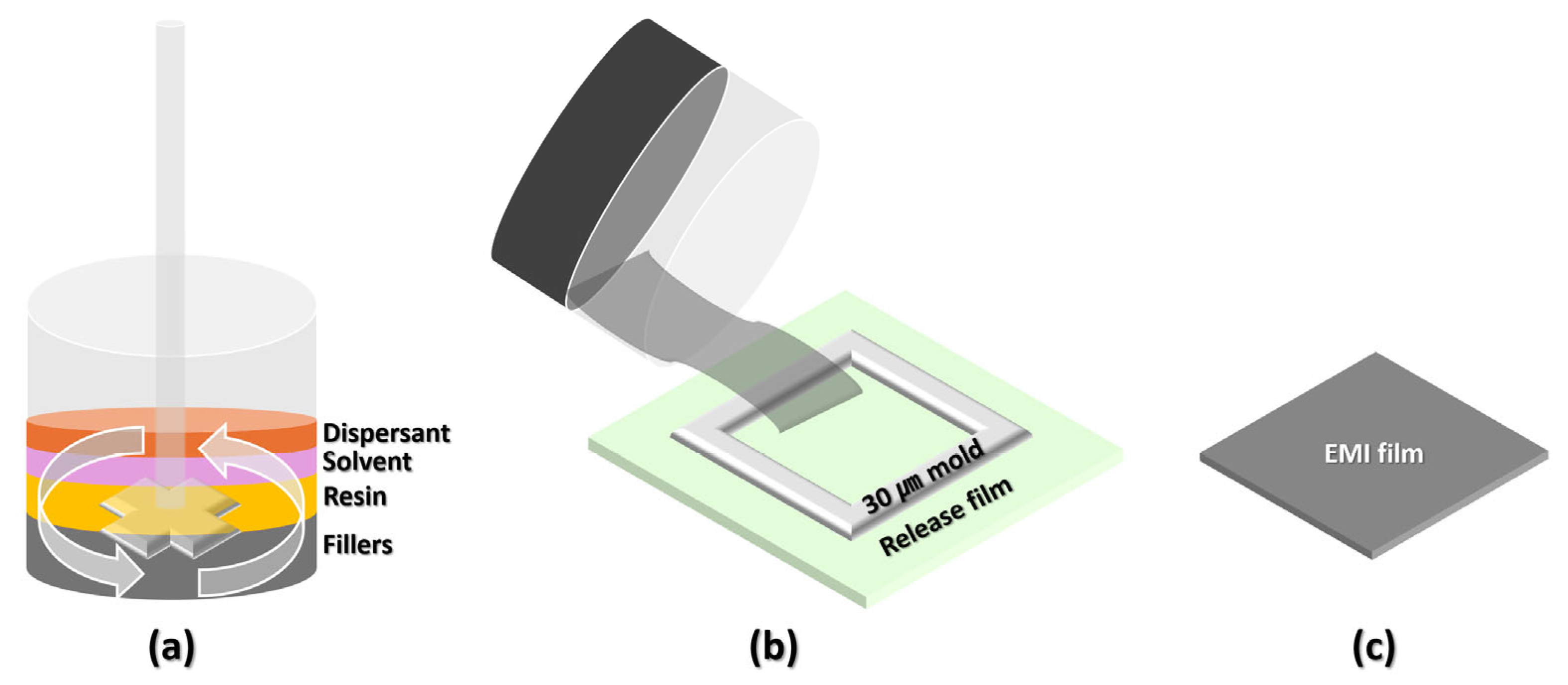
Table 1 presents the formulation of the trimodal silver ink in terms of its weight ratio. The ink was mixed and dispersed according to this ratio, as shown in
Figure 1a. Subsequently, a 30 μm thick mold was used for the film-forming process on a release film, as illustrated in
Figure 1b. The trimodal silver ink was first dried at 110 °C for 60 min, followed by a curing process at 140 °C for 90 min. The curing conditions were determined based on thermogravimetric analysis (TGA) and differential thermal analysis (DTA).
After the curing process was completed, the EMI film was detached from the release film, finalizing the fabrication process. Various material properties were measured to obtain essential data for package structure analysis. First, the resistance variation in the EMI film was observed when attached to a chip via thermal lamination. To investigate the cause of resistance changes, the film’s microstructure was analyzed using Field Emission Scanning Electron Microscopy (FE-SEM) (VEGA3, Tescan Ltd., Brno, Czech Public). In addition to electrical conductivity, thermal dissipation properties were evaluated using the LFA (LFA 467 Hyper Flash, NETZSCH Co., Ltd., Selb, Germany). Furthermore, to assess the mechanical durability of the EMI film, both a single bending test and a cyclic bending test were performed. The cyclic test was conducted at a bending radius of 4 mm for up to 1000 cycles, during which the normalized resistance change (ΔR/R0) was monitored to evaluate electrical stability under repeated mechanical stress. Finally, the SE of the EMI film was measured, and the obtained values were used as the basis for design optimization.
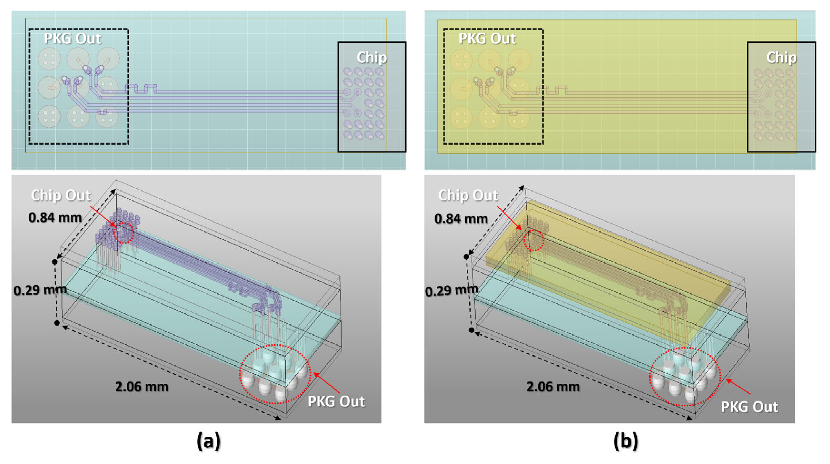
Based on the analysis and measurement results, a simulation study was conducted to assess the applicability of the EMI shielding film in semiconductor packaging processes. In particular, the study focused on mitigating crosstalk between differential signal lines, which is a crucial factor in high-speed signal transmission. To achieve this, the 3W Rule, a widely used guideline for reducing crosstalk, was considered [
40]. According to the 3W Rule, the spacing between adjacent signal lines should be at least three times the signal line’s width to effectively suppress crosstalk. However, in advanced packaging technologies, where miniaturization and high integration are required, maintaining strict compliance with the 3W Rule is often challenging due to limited space constraints. To address this issue, the feasibility of applying an EMI shielding film to minimize crosstalk was explored. Instead of ensuring sufficient spacing between the signal lines, this study investigated whether EMI shielding could compensate for non-compliance with the 3W Rule. To validate this approach, a non-compliant model was designed, where the spacing between differential signal lines was set to 1.5W rather than the conventional 3W, and the performance was compared between models with and without the EMI shielding film. The signal routing, spanning from chip I/O to package I/O, was designed using the Altium CAD Tool, and a three-dimensional electromagnetic simulation was performed to evaluate signal integrity in high-speed transmissions. The key specifications of the package design included a chip pad size of 40 μm and a pad pitch of 55 μm, with signal traces shorter than 2 mm to comply with UCle 1.0 standards. Additionally, the package ball pad size was 150 μm, following the BGA Land Pattern IPC standard. To minimize the skew caused by ball placement, the differential signal lines were designed with equal lengths, ensuring signal integrity. However, as the model did not fully comply with the 3W Rule, there remained a potential risk of signal interference. To mitigate this issue, an EMI shielding film was applied, and simulations were conducted using Ansys SIwave to evaluate its effectiveness. As shown in
Figure 2a, the model without the EMI shielding film exhibited crosstalk, as expected, due to insufficient signal line spacing. In contrast,
Figure 2b depicts the model with the EMI shielding film applied to the top surface, demonstrating an alternative shielding approach despite non-compliance with the 3W Rule. To quantify the impact of the EMI shielding film, signal transmission characteristics were analyzed through various simulations. The key parameters included S-parameter (S31, S41) analysis to evaluate crosstalk, eye diagram comparison to assess signal integrity and noise characteristic assessments. The results confirmed that the EMI shielding film effectively suppressed crosstalk, thereby maintaining signal integrity even when the 3W Rule was not fully followed. This suggests that EMI shielding can be a viable solution for high-density semiconductor packaging, enabling improved signal integrity without requiring large signal line spacings.
3. Results and Discussion
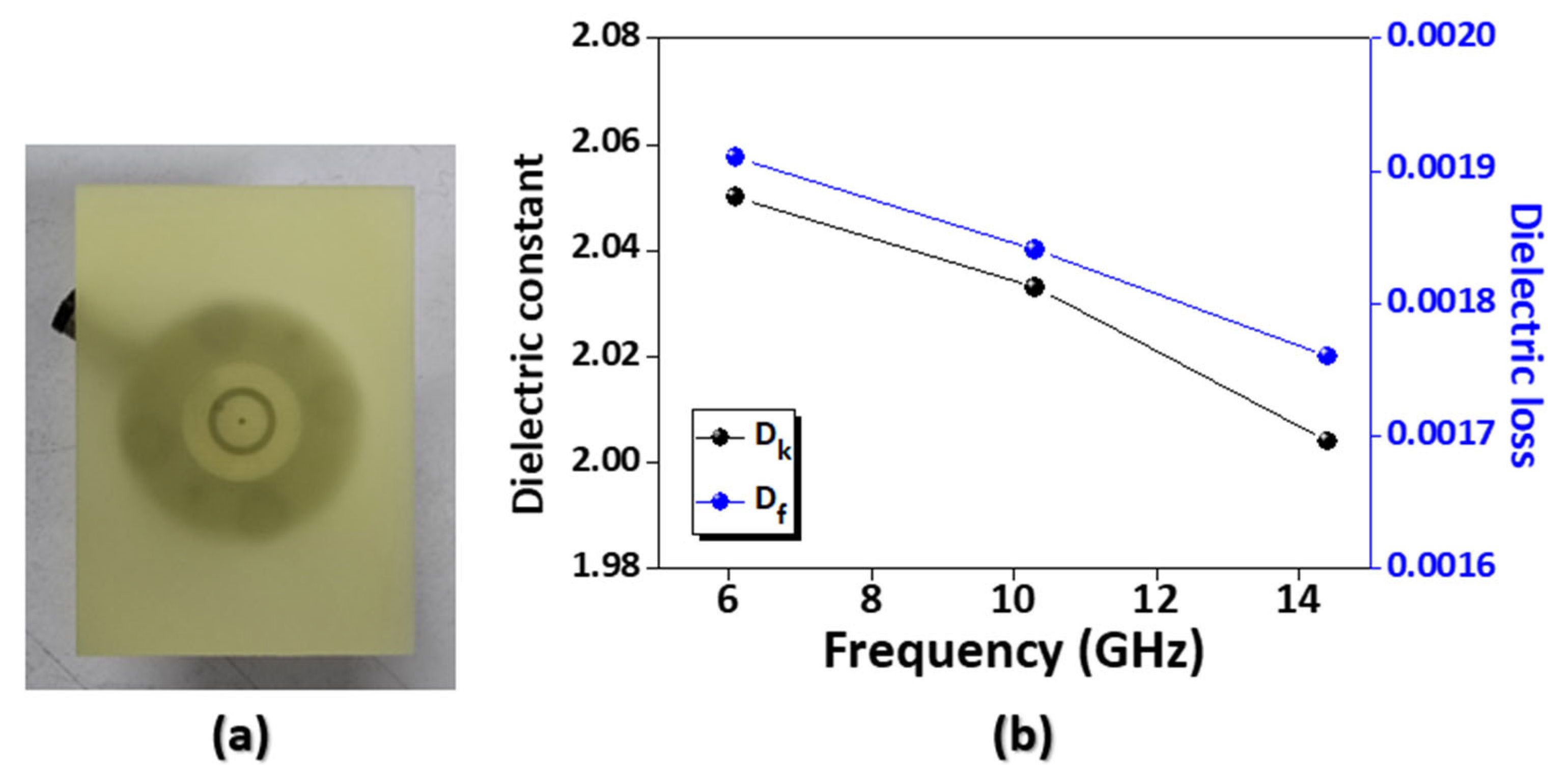
To verify the low-dielectric properties of the PI resin used as the matrix material, its D
k and D
f were measured over the 6.1–14.4 GHz frequency range.
Figure 3a presents an image of the PI sample during the measurement process, utilizing an Open Coaxial Resonator (AET Inc., Japan) to obtain the actual D
k and D
f values. The corresponding measurement results are graphically represented in
Figure 3b. To optimize the measurement conditions, the PI sample was fabricated with a thickness of 200 μm. The measurement results indicated that at 6.1 GHz, the D
k and D
f were 2.05 and 0.0019, respectively, while at 10.3 GHz, the values were 2.033 and 0.00184, and at 14.4 GHz, they further decreased to 2.004 and 0.00176. An analysis of the results revealed a gradual decrease in the D
k with increasing frequency, which aligns with the general behavior of dielectric materials in high-frequency ranges, where the polarization response weakens. Similarly, the D
f also exhibited a decreasing trend with increasing frequency, suggesting that the PI resin possesses low-loss characteristics, making it suitable for RF and high-frequency applications. Notably, the dielectric properties of this PI material exhibited lower values compared to those reported in previous studies on conventional PI materials [
41,
42,
43]. This indicates that the PI resin used in this study can offer enhanced signal transmission performance, minimizing signal loss in package substrates and high-frequency circuit designs.
To investigate the thermal behavior of both the uncured ink and the cured EMI film, thermogravimetric analysis (TGA) and differential thermal analysis (DTA) were conducted, as shown in
Figure 4. The ink exhibited a marked weight loss below 150 °C due to solvent evaporation, as confirmed by the TGA curve (gray) and a corresponding endothermic transition in the DTA profile (purple). In contrast, the cured EMI film displayed minimal weight loss of up to 300 °C (black), indicating excellent thermal stability. The film’s DTA curve (blue) also showed an endothermic transition near 250 °C, corresponding to thermal activation during the lamination process. These results demonstrate that the EMI film retains its structural integrity under elevated thermal conditions and is suitable for high-temperature applications.
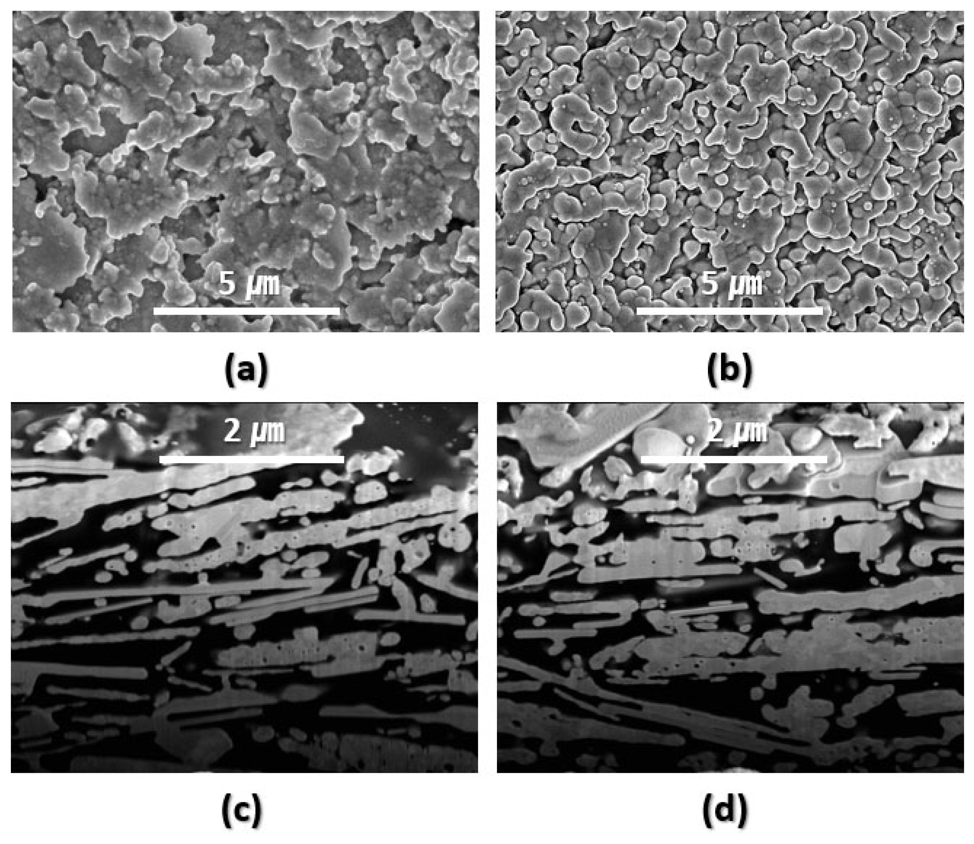
The vacuum lamination process was conducted at 180 °C for 1 h, and the microstructural changes in the EMI film before and after lamination were evaluated using FE-SEM. Figure 6a presents the FE-SEM image of the EMI film before lamination, while Figure 6b shows the FE-SEM image after the lamination process. As observed in Figure 6a, the surface of the pre-laminated EMI film appeared relatively rough and non-uniform, with an irregular distribution of Ag particles. The interparticle connections were incomplete, which may have limited the formation of continuous electrical pathways. In contrast, Figure 6b illustrates the surface morphology of the post-laminated EMI film, where the contact area between the Ag particles increased, and a more uniform conductive network was formed. This microstructural improvement was attributed to the enhanced adhesion between Ag particles and partial particle rearrangement during the lamination process. These microstructural changes are one of the primary factors contributing to the enhancement of electrical conductivity. As the conductive pathways within the EMI film expand during lamination, the overall electrical conductivity increases by approximately 50%, as shown in
Figure 5. This confirms that the lamination process employed in this study effectively improves the electrical performance of the EMI film, making it a viable approach for enhancing EMI shielding applications.
The vacuum lamination process was conducted at 180 °C for 1 h, and the microstructural changes in the EMI film before and after lamination were analyzed using FE-SEM.
Figure 6a presents the FE-SEM image of the EMI film before lamination, while
Figure 6b shows the image after the lamination process. As observed in
Figure 6a, the pre-laminated EMI film exhibits rough and non-uniform surface morphology, with an irregular distribution of Ag particles. The interparticle connections appear incomplete, potentially limiting the formation of continuous electrical conduction pathways.
In contrast,
Figure 6b illustrates the surface of the post-laminated EMI film, where the contact area between Ag particles increased, forming a more uniform and interconnected conductive network. This microstructural improvement could be attributed to enhanced adhesion between Ag particles and partial particle rearrangement during the lamination process.
Figure 6c,d present cross-sectional SEM images of the EMI film before and after lamination, respectively. In
Figure 6c, the internal structure shows sparse vertical alignment and weak interfacial contact between the Ag particles. After lamination (
Figure 6d), the internal microstructure became denser and more layered, indicating anisotropic alignment and stronger interconnectivity. These features are closely associated with improved electron transport paths and directional thermal conductivity.
These structural modifications collectively contribute to an approximately 50% increase in electrical conductivity. These findings confirm that the lamination process employed in this study effectively enhances the electrical performance and internal structural integrity of the EMI film, making it a promising approach for high-performance EMI shielding applications.
When shielding materials are applied in electronic devices, the issues of miniaturization, high performance, and high integration often lead to increased heat generation, making thermal dissipation a critical factor. Therefore, in this study, the thermal conductivity of the laminated EMI film was measured using LFA to evaluate its heat dissipation performance.
Table 2 summarizes the physical properties required for thermal conductivity analysis, including density, specific heat capacity, and thickness. The density was measured using the Archimedes method, yielding an average density of 5.069 g/cm
3 and a specific heat capacity of 0.407 J/g·K. Based on these properties, the thermal diffusivity and thermal conductivity were analyzed in both vertical and horizontal directions, revealing distinct anisotropic heat transfer characteristics. The thermal diffusivity and thermal conductivity in the vertical direction were measured as 4.968 mm
2/s and 10.249 W/m·K, respectively. In contrast, in the horizontal direction, the thermal conductivity was 34.614 W/m·K under isotropic conditions and 18.836 W/m·K under anisotropic conditions. Comparatively, the horizontal thermal conductivity was approximately 3.4 times higher than the vertical direction under isotropic conditions and 1.8 times higher under anisotropic conditions. Notably, the 45.6% reduction in horizontal thermal conductivity under anisotropic conditions, compared to isotropic conditions, clearly illustrates the influence of internal structural anisotropy on heat transfer characteristics. These results indicate that the primary heat conduction pathways are predominantly formed in the horizontal direction, highlighting the necessity of optimizing heat dissipation performance in specific directions during material design. The thermal conductivity measurements in both vertical and horizontal directions were performed under standard conditions, using sample holes of 12.7 mm and 25.4 mm to ensure measurement accuracy. Materials exhibiting high horizontal thermal conductivity play a crucial role in next-generation semiconductor and packaging technologies. In particular, high-power semiconductor devices, high-frequency (RF) packages, and high-performance transistors generate substantial heat during operation, making efficient heat dissipation essential. The spread of rapid heat across the chip surface can reduce hotspot formation, ensuring stable transistor switching speeds and power efficiency. Additionally, effective thermal management in compact and high-density designs can enhance system reliability. In 3D stacking structures and Chiplet-based architecture, this material can help balance heat distribution between chips, acting as an efficient heat spreader to improve overall thermal performance.
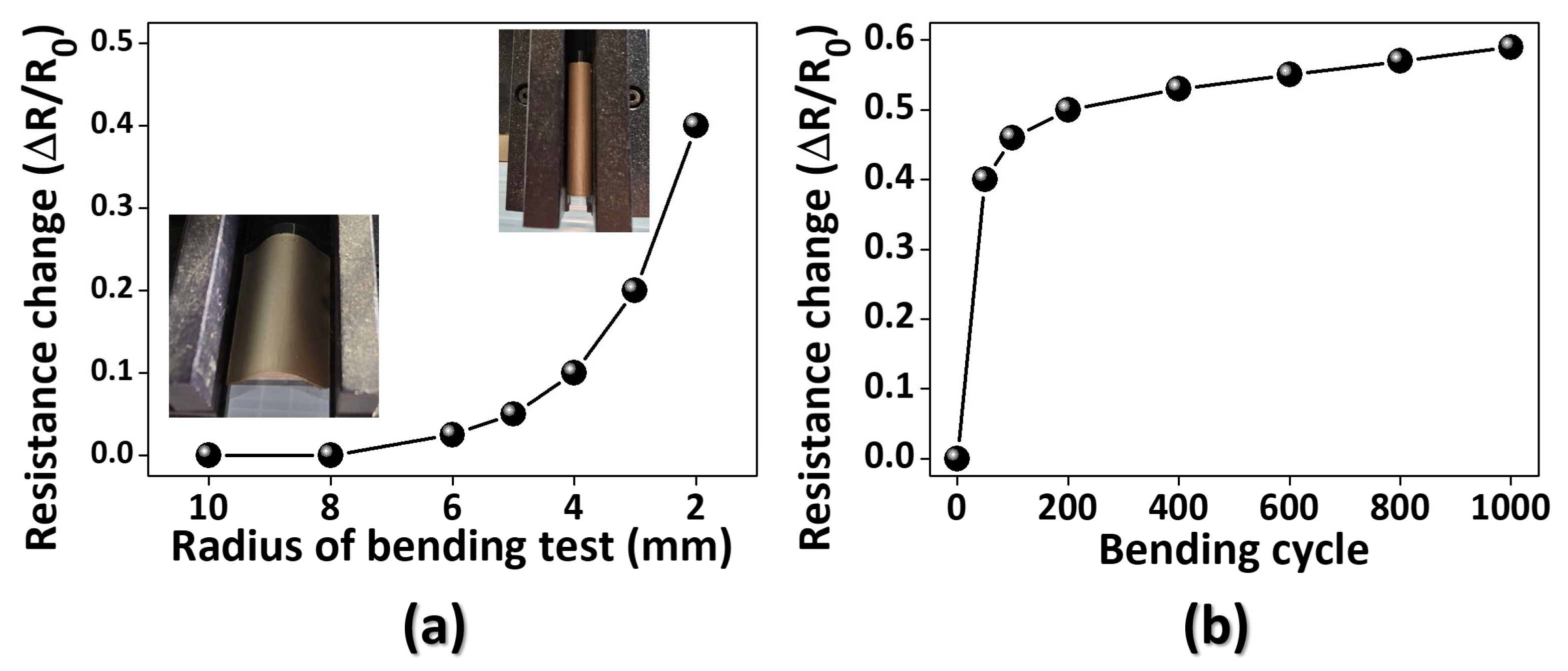
To assess the flexibility and structural stability of the EMI film, which was verified for its high thermal and electrical conductivity, a bending test was conducted. The experiment applied gradual deformation at a constant speed of 0.5 mm/s, reducing the radius of curvature from 10 mm to 2 mm. Additionally, a cyclic bending test was performed at a fixed curvature radius of 4 mm, and the same speed of 0.5 mm/s was used to evaluate durability under repeated deformation.
Figure 7 presents the results of the bending test, illustrating the resistance variation as a function of the curvature radius and bending cycle. The initial resistance was measured at 0.4 Ω, and at a 10 mm curvature radius, the electrical resistance remained nearly unchanged at 0.4 Ω, indicating minimal resistance variation due to mechanical deformation. As the curvature radius progressively decreased, a slight increase in resistance was observed. However, even at the smallest curvature radius of 2 mm, the resistance increased by only approximately 0.4 times the initial value, confirming that the EMI film maintained excellent flexibility and structural integrity. Furthermore, during the cyclic bending test conducted at 4 mm, the relative resistance change remained below 0.6 even after 1000 cycles, confirming that the film preserved electrical stability and mechanical durability under prolonged stress. These findings suggest that the uniform distribution and high adhesion of Ag particles within the EMI film play a crucial role in stabilizing the internal conductive pathways during deformation, ensuring consistent electrical performance even under mechanical stress.
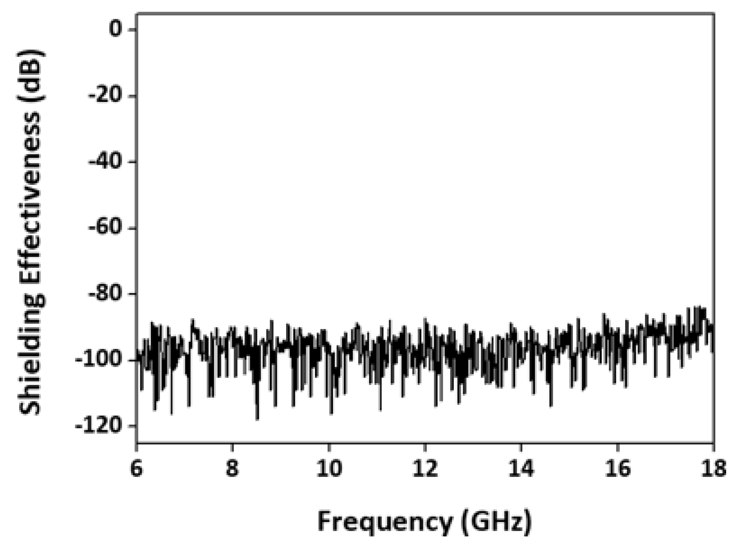
To evaluate the SE of the EMI film, which was verified for its excellent flexibility, electrical conductivity, and thermal conductivity, a high-frequency electromagnetic shielding effectiveness measurement was conducted. The measurements were performed using a vector network analyzer (VNA) (MS4647B, Anritsu Co., Atsugi, Japan) in conjunction with a high-frequency shielding effectiveness measurement system (GPC7-ES7, KEYCOM Co., Tokyo, Japan). The measurement of the frequency range was set from 6 GHz to 18 GHz, covering the X-band (8–12 GHz). The shielding effectiveness measurement process began with cutting the sample into a size suitable for the test model using a precision sample cutter. Following this, a TECOM-certified USB was connected to the PC, and the measurement program was executed. The test frequency range and data points were set to complete the initial measurement setup. VNA calibration was carried out using a K-type calibration kit, performing open, short, and load calibrations. After connecting the measurement cables, a Thru calibration was conducted to ensure measurement accuracy.
Figure 8 presents the recalculated SE based on the transmission coefficient S
21 over the 6–18 GHz frequency range. The SE was derived using the relation of SE (dB) = −20 log
10 ∣S
21∣, and the results showed a consistent SE range between 80 and 120 dB, with an average value of approximately 100.08 dB. These findings demonstrate that the EMI film exhibits outstanding electromagnetic shielding performance in high-frequency ranges, confirming its potential as a high-performance shielding material capable of effectively suppressing strong EMI.
To evaluate the FEXT and NEXT characteristics of a structure incorporating the EMI shielding film, simulations were conducted using Ansys SIwave, and the results are presented in
Figure 9. The graph illustrates the variations in S-parameters for NEXT and FEXT over a 0–40 GHz frequency range, comparing models with and without the EMI shielding film. The analysis revealed that in the absence of the EMI shielding film, the interference levels for NEXT and FEXT were relatively lower at lower frequencies. However, when the EMI shielding film was applied, a significant suppression of interference was observed as the frequency increased. Notably, the application of the EMI shielding film resulted in a reduction in NEXT and FEXT interference by approximately 6 dB up to 35 GHz, indicating a substantial improvement in signal integrity (SI) for high-frequency signal transmissions. These results confirm that the EMI shielding film is highly effective in suppressing crosstalk in advanced semiconductor packaging, positioning it as a key technology for high-density, high-speed signal design. In particular, in highly integrated environments where the pad-to-pad pitch is limited to 25–55 μm, the EMI shielding film presents a viable alternative to traditional shielding vias, offering a solution that simultaneously enhances signal performance and maximizes space efficiency.
Figure 10 presents the results of the signal integrity (SI) analysis, where the data transmission rate was set to 10 Gbps per data channel, and the rise/fall time was configured as 30 ps, corresponding to 30% of the unit interval (UI). The experiment aimed to evaluate the impact of crosstalk on eye diagram characteristics before and after applying the EMI shielding film, comparing the signal quality under different conditions. The analysis results indicate that before applying the EMI shielding film (
Figure 10a,c), significant NEXT and FEXT interference was observed, leading to narrow eye-opening and poor signal stability. Specifically, in
Figure 10a, the voltage amplitude was measured at only 2.78 mV, demonstrating severe signal integrity degradation. Similarly, in
Figure 10c, a high interference level of 22 mV was detected, indicating the high probability of data transmission errors due to intense signal coupling between adjacent traces. In contrast, after applying the EMI shielding film (
Figure 10b,d), both NEXT and FEXT interferences were significantly reduced, resulting in wider eye-opening and an improved voltage amplitude, enhancing overall signal integrity. In
Figure 10b, NEXT interference was mitigated, leading to a voltage amplitude improvement of 0.75 mV, while in
Figure 10d, FEXT interference was substantially reduced, with the voltage amplitude decreasing to 7.1 mV. These improvements indicate that the EMI shielding film effectively enhances signal quality, enabling stable high-speed data transmission. Notably, the results from
Figure 10b,d exhibit a signal quality comparable to that achieved using the conventional 3W Rule, confirming that the EMI shielding film can effectively suppress signal interference while remaining compatible with ultra-compact, high-density package designs. Furthermore, applying the EMI shielding film to a package containing 32 high-speed signal lines allowed the signal line spacing to be reduced from 3W to 1.5W, achieving a 50% reduction in package size while effectively minimizing signal interference. These findings highlight the EMI shielding film as a next-generation packaging solution, offering both space efficiency and enhanced signal quality. Ultimately, the developed EMI film reduced NEXT interference by 77.8% and FEXT interference by 65%, demonstrating a significant improvement in overall signal performance.
4. Conclusions
In this study, an EMI shielding film based on trimodal Ag ink was developed and evaluated from multiple perspectives to assess its potential applications in high-speed signal packaging and electromagnetic shielding. First, dielectric property analysis confirmed that the low-dielectric PI-based EMI film exhibited a lower Dk (2.004) and Df (0.0019) compared to conventional PI materials, demonstrating its suitability for high-frequency signal transmission. Additionally, the thermal analysis (TGA-DTA) and lamination process evaluation verified that the EMI film maintained thermal stability at high temperatures while also being designed for lamination at a specific activation temperature (250 °C). Electrical property analysis revealed that after lamination, the electrical conductivity of the EMI film increased by 50% (from 0.752 105 S/m to 1.13 × 10⁵ S/m), which was attributed to the rearrangement and improved adhesion of metal particles during this process. FE-SEM analysis further confirmed that the increased contact area between Ag particles after lamination led to the formation of a more uniform conductive network, contributing to enhanced electrical performance. The evaluation of thermal conductivity showed that the horizontal thermal conductivity of the EMI film (34.614 W/m·K) was 3.4 times higher than vertical thermal conductivity (10.249 W/m·K), demonstrating its effectiveness in heat dissipation for high-density packaging and 3D stacking architectures. The flexibility assessment via bending tests indicated that even at a curvature radius of 2 mm, the resistance increased by only 0.4 times the initial value, confirming excellent flexibility and structural stability. Moreover, in cyclic bending tests conducted at a 4 mm curvature radius for 1000 cycles, the normalized resistance change remained below 0.6, verifying outstanding mechanical durability and long-term electrical stability under repeated deformation. SE measurements showed that the EMI film maintained an average shielding effectiveness of 99.7 dB in the 6–18 GHz frequency range, highlighting its outstanding EMI shielding performance in high-frequency applications. Furthermore, NEXT and FEXT crosstalk simulation results demonstrated that applying the EMI shielding film reduced crosstalk by approximately 6 dB and up to 35 GHz, effectively mitigating signal interference even in miniaturized, high-speed packaging environments. Eye diagram analysis further confirmed that NEXT interference was reduced by 77.8% and FEXT interference was reduced by 65%, leading to a significant improvement in signal quality. Notably, the EMI shielding film provided crosstalk suppression comparable to the conventional 3W Rule, even without strict compliance with the rule. This suggests that applying the EMI shielding film to a package containing 32 high-speed signal lines enables the signal line spacing to be reduced from 3W to 1.5W, allowing for a 50% reduction in the package size while effectively minimizing signal interference. In conclusion, the developed EMI shielding film exhibited excellent electrical conductivity, flexibility, thermal dissipation, mechanical durability, and electromagnetic shielding performance, making it a high-performance material. Its potential applications are particularly promising in high-frequency circuits, 5G and mmWave communications, high-speed signal packaging, and advanced semiconductor packaging, where high-density integration and signal integrity are critical.


 ,
, 


