1. Introduction
Cu
2ZnSnS
4 (CZTS) is a quaternary tin-, zinc- and copper-based sulfur thin film semiconductor. It has attracted significant interest as an absorber layer for photovoltaic (PV) devices due to the low cost, availability, and eco-friendly nature of its materials. CZTS is a more sustainable choice than Cu(In,Ga)Se
2 (CIGS) for large-scale solar cell fabrication, since CIGS comprises relatively expensive and uncommon indium and gallium [
1]. CZTS possesses the suitable direct band gap of 1.4–1.6 eV and high optical absorption coefficient and is a promising candidate for thin-film solar applications. The majority of incident solar energy is usually absorbed by a CZTS absorber layer between 1 and 2.5 μm thick, resulting in effective photovoltaic conversion [
2].
The growth mechanisms, absorber-layer chemistry, and manufacturing circumstances of CZTS thin films have been studied by several research groups. Lower production costs, reduced material waste, and better scalability for large-scale manufacturing have increased interest in non-vacuum deposition techniques [
3]. Electrodeposition is one of these approaches; it is straightforward, inexpensive, compatible with large-area substrates, and is suited for high-throughput production. By modifying the bath chemistry, applied potential or current density, pH, agitation, and deposition period, electrodeposition also enables better control of the precursor composition [
4].
CZTS electrodeposition is typically carried out by either sequential electrodeposition of metallic precursor layers followed by sulphurization or selenization, or one-step co-electrodeposition of Cu, Zn, Sn, and S-containing species. However, because Cu, Zn, and Sn have distinct reduction potentials and deposition rates, regulating their simultaneous deposition is still difficult. Zinc requires higher cathodic potentials at which hydrogen evolution may occur, although copper is more readily reduced than zinc and tin. Rough morphology, poor adhesion, pinholes, compositional deviation, and secondary-phase development are possible outcomes. To achieve compact and homogeneous CZTS films, it is crucial to carefully regulate the electrolyte composition, current density, pulse timing, pH, complexing agents, and mass transfer [
4,
5,
6,
7].
Another crucial stage in the creation of superior CZTS absorber layers is post-deposition thermal treatment. Sulphurization or selenization is typically necessary to enhance crystallization, grain growth, phase formation, and absorber composition, as electrodeposited CZTS precursor films often exhibit low crystallinity [
8]. The kesterite CZTS phase is created during sulphurization when sulfur combines with electrodeposited Cu–Zn–Sn precursors. However, if the precursor composition or annealing conditions are not properly controlled, unwanted secondary phases, including Cu
2S, ZnS, SnS, SnS
2, and Cu
2SnS
3, may develop. By boosting recombination, decreasing carrier collection, and lowering open-circuit voltage and fill factor, these secondary phases can have a detrimental impact on device performance [
9,
10,
11].
Numerous investigations have demonstrated that the Cu/(Zn + Sn), Zn/Sn, and S/(Cu + Zn + Sn) ratios have a significant impact on the final characteristics of CZTS thin films. A slightly Cu-poor and Zn-rich composition is commonly desired for high-grade CZTS absorbers, as it improves device performance and reduces the formation of conductive Cu-based secondary phases. Otherwise, Sn-poor or Sn-rich conditions can result in undesirable tin sulfide phases. Cu-rich films can promote the formation of Cu
2S. Thus, composition optimization is one of the most important criteria for forming thick, homogeneous, and phase-pure CZTS absorber layers [
12,
13,
14,
15].
Pulse electrodeposition has been proposed as a promising method to enhance control over the electroplating process and improve the quality of CZTS thin films. Pulse electrodeposition alternates between deposition and relaxation periods, in contrast to direct-current electrodeposition. Metal ions are reduced and deposited onto the substrate during the pulse-on period, while ion redistribution occurs near the electrode surface during the pulse-off period [
16]. As a result, concentration polarization is lessened, hydrogen evolution is suppressed, ion replenishment is enhanced, and more uniform film growth is encouraged. Consequently, after thermal treatment, pulse electrodeposition can yield CZTS films with superior compactness, fewer microcracks, higher compositional homogeneity, and increased crystallinity [
16,
17,
18].
In CZTS electrodeposition, mass transport and agitation are also significant factors. It is challenging to comprehend the relationship between ion transport, reaction kinetics, film composition, and shape because deposition has frequently been done under ill-defined hydrodynamic conditions [
19,
20,
21]. A helpful approach for researching CZTS electrodeposition under regulated mass-transfer settings is the rotating disc electrode (RDE) technique. The transport rate of electroactive species to the electrode surface can be regulated by varying the rotation speed, thereby enabling a more systematic examination of the effects of current density, pulse timing, and electrolyte dilution on film growth [
22,
23,
24].
Despite extensive research, a number of unanswered questions remain about CZTS electrodeposition. These include the development of hydrogen gas at high cathodic current densities, the creation of secondary phases, the uneven integration of Zn and Sn, the poor crystallinity of as-deposited films, and the challenge of attaining large-area compositional uniformity [
25]. Diluted electrolytes, in particular, may help reduce excessive deposition rates, enhance surface morphology, and provide greater control over film composition. Nevertheless, it remains unclear how the dilution of the electrolyte composition and pulsed-current parameters interact [
26,
27,
28].
Therefore, the main objective of this study was to systematically examine how diluted electrolyte composition, current density, and pulse timing affect CZTS film growth, morphology, composition, and optical properties, rather than to maximize solar-cell performance [
29]. Furthermore, the goal of this work is to demonstrate that functional CZTS-based photovoltaic systems can be produced under diluted, simplified electrodeposition conditions. The study promotes the development of low-cost, scalable, solution-based fabrication techniques for CZTS thin-film solar cells and sheds light on the function of mass transport and pulsed-current management in enhancing CZTS absorber quality [
30,
31].
Deposition of CZTS from electrolytes with relatively high concentrations has been described in our earlier work. We therefore intentionally use an electrolyte with an ionic strength ten times lower than that typically used in such studies, and test whether such a low-ionic-strength solution can nevertheless yield dense, stoichiometric absorbers suitable for device manufacturing. Previous research on CZTS electrodeposition has generally used single bath electrolytes with metal precursor concentrations in the range of ~10–80 mM depending on bath chemistry, sulphur source, complexing agent and pH conditions. For example, the Cu, Zn, Sn and sulphur precursor concentrations in some reported CZTS electrodeposition baths were on the order of 10–20 mM or more. In contrast, this study employs a very dilute electrolyte containing 5.1 mM CuSO
4, 3.4 mM ZnSO
4, 4.6 mM SnCl
2, and 0.44 M Na
2S
2O
3, which translates to a far lower metal ion concentration than many prior CZTS electrodeposition systems. Therefore, the originality of this work is not only the use of a diluted bath but also the systematic combining of electrolyte dilution with the optimization of the pulse current. In this work, the influence of short and long pulse conditions on the effects of ion replenishment, hydrogen evolution, composition control, crystallinity, surface morphology and photovoltaic behavior of the resulting CZTS absorber layers is investigated by altering the current density and pulse-on/off time [
32,
33,
34,
35,
36,
37].
In this study, we apply a comparable approach to the previously used diluted method, resulting in significantly enhanced deposit characteristics [
7]. Moreover, the effect of hydrogen co-evolution on the electrodeposition of CIGS is studied by assessing the hydrogen current density versus the precursor and total current densities during alloy reduction.
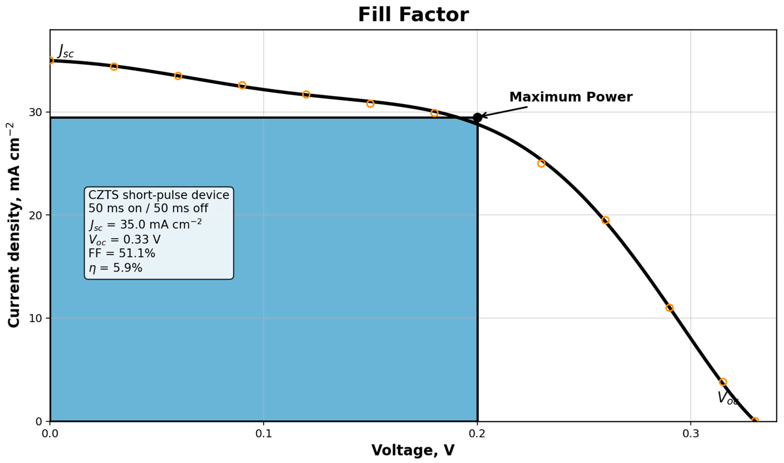
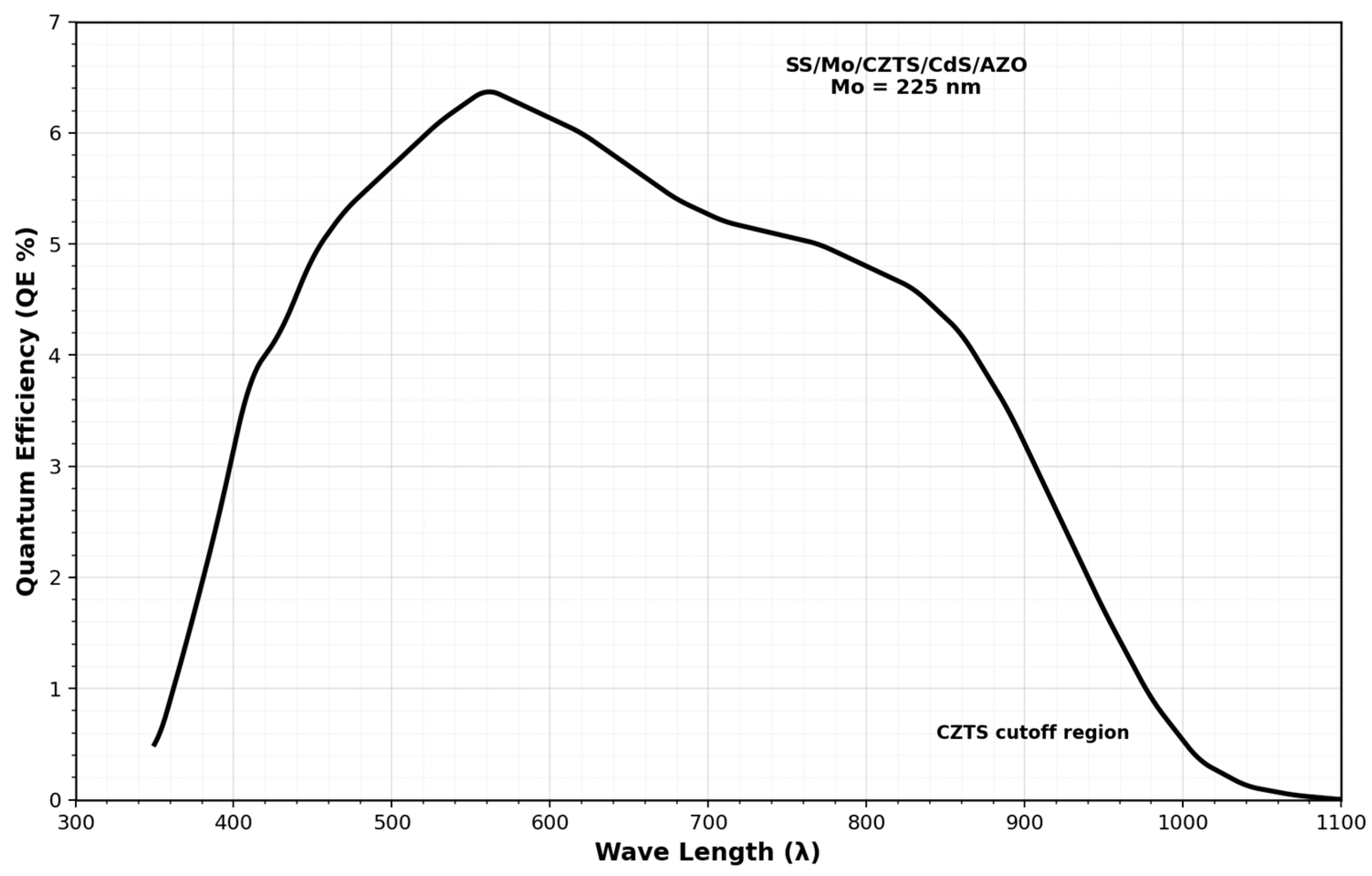
The CZTS absorber layer, as well as the complete photovoltaic device, has been manufactured solely by electrodeposition. The device consists of the following layers: stainless steel/Ni/Mo/CZTS/CdS/ZnO/ZnO-Al. To characterize the integrated photovoltaic device, the quantum efficiency was determined with a solar simulator. The identified parameters include the fill factor, band gap, open-circuit voltage, short-circuit current and overall efficiency.
2. Specifics of the Experiment
Electrodeposition was performed on a commercial rotating disc electrode (RDE) system A Bio-Logic USA, Knoxville, TN potentiostat/galvanostat Model VSP was used with a motor controller to control the working electrode rotation speed, and a standard three-electrode electrochemical cell setup. The device was a 0.32 cm2 stainless steel (406 SS) electrode covered with a 99.95% Mo molybdenum layer by electron-beam physical vapor deposition. The operation was carried out in a vacuum atmosphere at 2 × 10⁻⁶ torr. The deposition rate was reduced to 0.3 Å/s to compensate for the effects of elevated equipment temperatures. Thereafter, the sputtering process was performed for 60 min to an approximate thickness of one μm. The disc was then flush-embedded in an insulated Teflon cylinder. The reference electrode was a saturated calomel electrode (SCE), and the counter electrode was a platinum lattice. The electrochemical solutions under investigation are contained in a 50 mL beaker and are filled with electrodes. The pH of the electrolyte was adjusted to 1.85 by addition of hydrochloric acid. Experiments were performed at an ambient temperature of 20 °C with rotation rates from 0 to 600 rpm.
To increase adherence, the stainless-steel disc was electro-activated for a few seconds at 1.8 V vs. NHE in 0.2 M H2SO4 (Sigma-Aldrich, St. Louis, MO, USA) before electroplating. The bath composition was 5.1 mM CuSO4 (Sigma-Aldrich, 99.9%), 3.4 mM ZnSO4 (Sigma-Aldrich, 99.9% trace metals base), 4.6 mM SnCl2 (Strem-Chemicals, Newburyport, MA, USA, 99.9%), 0.44 M Na2S2O3 (Sigma-Aldrich, 99% Reagent Plus). The buffer was diluted to 100 mL with purified water, and each bag contained a precise buffer solution. The electrolyte was buffered to pH 2 using Hydrion pH buffer solution and 0.69 M LiCl and incorporated into the bath as a supporting electrolyte. All compounds were obtained from Sigma-Aldrich (St. Louis, MO, USA).
The above-specified electrolyte ranges were investigated to determine the optimal film composition and performance. The studies were performed potentiostatically, with electrodeposition potentials ranging from −0.8 to −1.1 V vs. NHE. This implies that the electrodeposition voltage equals the reference electrode potential on the scale (0 V versus NHE = 0.242 V vs. SCE).
The experimental design was clarified by separating the preparatory bath-composition adjustment and the pulsed-current comparison. Initially, only a few diluted electrolyte compositions were studied to obtain a final CZTS composition close to the ideal stoichiometric ratio. After determining the most suitable diluted solution, the pulsed-current investigation was mainly conducted by adjusting the pulse-on and pulse-off duration. Other factors such as electrolyte type, pH, RDE rotation speed, substrate, deposition temperature and post-deposition annealing conditions were kept as consistent as feasible. Only small fluctuations in current density were used to keep the electrodeposition steady under each pulse regime. The major purpose of this work is to investigate the effect of pulse time on the morphology, crystallinity, composition uniformity and device performance of CZTS film under diluted-electrolyte circumstances.
In this work, additional layers were electrodeposited on the CZTS film to fabricate the full PV device. The CZTS absorber was coated with a 50 nm thick CdS starting layer. The electrodeposition of cadmium sulfide was performed at a temperature of 67 °C in an electrolyte containing 0.3.1 M CdCl2, 7.2 mM Na2S2O3, and 0.6 M KCl. The bath was replaced with 2 M HCl. The electrolyte was maintained at −0.8V vs. SCE for 15 min. This was followed by a 170 nm deposition of an undoped, transparent electroplated zinc oxide layer. The layer was electrodeposited at −0.85 V vs. SCE for 45 min at 250 rpm at 70 °C from an electrolyte containing 0.2 M Zn(NO3)2 and 0.5 M KCl. NaOH was added to lower the bath pH to 6. Finally, the electrolyte of 0.2 M Zn(NO3)2, 0.95 mM InCl3 and 0.5 M KCl was used to deposit a 500 nm indium-doped zinc oxide window coating by applying −1.1 V vs. SCE for 50 min at 250 rpm and 75 °C. The pH buffer was adjusted to 3.5 using NaOH.
The final composition of the electrodeposit on the CZTS surface was studied using a Hitachi S-4500 scanning electron microscope (SEM), Tokyo, Japan, equipped with a Noran Energy-Dispersive Spectrometer (EDS). EDS spectra were obtained with a NORAN System SIX EDS detector (Thermo Fisher Scientific, Madison, WI, USA) mounted on a scanning electron microscope. The metal composition analysis of the cross-section of the CZTS film was performed using the Focused Ion Beam (FIB) technique on the FEI Helios NanoLab 650 Dual-Beam System, Hillsboro, OR, USA equipped with an EDS. The crystallography of CZTS was analyzed by X-ray diffraction (XRD) with a Bruker Discover D8 X-ray diffractometer, Karlsruhe, Germany, with Cu K alpha (α) (λ = 0.15406 nm) radiation as the source and a step size of 0.01°. The PV tests were performed using the QEX10 quantum efficiency measurement instrument, Boulder, CO, USA, and an Oriel Sol2A solar simulator, Irvine, CA, USA. Hence, the metrics taken for characterization are overall efficiency, quantum efficiency, open-circuit voltage, short-circuit current, dark current, band gap, and fill factor.
3. Results and Discussion
3.1. CZTS Electrodeposition
3.1.1. Electrodeposition Using CZTS
The electrodeposition of CZTS is hampered by large discrepancies in the standard reduction potentials and electrochemical behavior of Cu, Zn, Sn, and sulfur-containing species. In instance, zinc has a rather negative deposition potential, while copper and tin are more easily reduced [
36]. As a result, the efficient co-deposition of Cu–Zn–Sn precursors generally involves the employment of complexing agents, pulsed deposition, or carefully controlled electrolyte composition to limit preferential copper deposition and improve the inclusion of zinc and tin. Furthermore, the incorporation of sulfur is complex in the direct electrodeposition of CZTS, as sulfur-containing species may participate in chemical and electrochemical reactions, which could result in the formation of binary and ternary secondary phases such as Cu
2S, SnS, ZnS, and Cu
2SnS
3 before the formation of the kesterite CZTS phase [
35,
36,
37].
To elucidate the influence of agitation and to optimize plating conditions at different spinning disc electrode speeds (e.g., 100, 300, and 500 rpm [
5,
6]), polarization experiments can be performed. Mass transfer, complexation, and hydrogen evolution significantly influence the electrochemical behavior of the CZTS system, particularly at more negative cathodic potentials. Hydrogen evolution competes with the reduction of metal ions, thereby lowering the current efficiency of targeted CZT or CZTS deposition. This is achieved by comparing the experimental polarization data with the expected limiting currents for Cu, Zn, Sn, and sulfur species at different potentials, thereby identifying the species controlled by mass transport and kinetic constraints. Copper reduction reaches its limiting current quickly, whereas zinc and tin incorporation are more sensitive to the applied voltage, pulse conditions, electrolyte pH, and the presence of complexing agents in a typical CZTS electrodeposition system. These variables must be optimized to produce a homogeneous Cu–Zn–Sn precursor with the Cu-poor, Zn-rich composition required for subsequent sulphurization and the formation of high-grade kesterite CZTS absorber layers [
8].
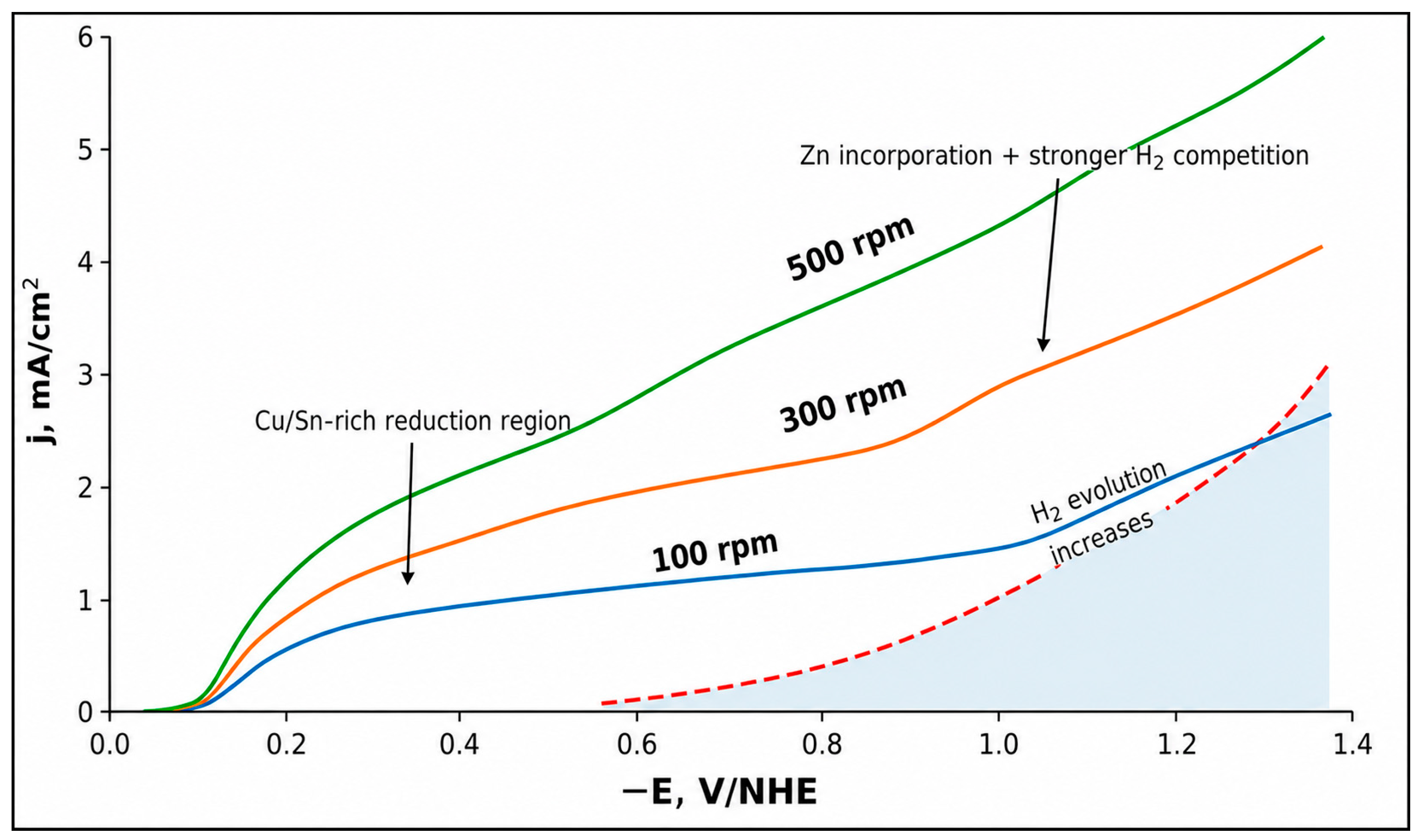
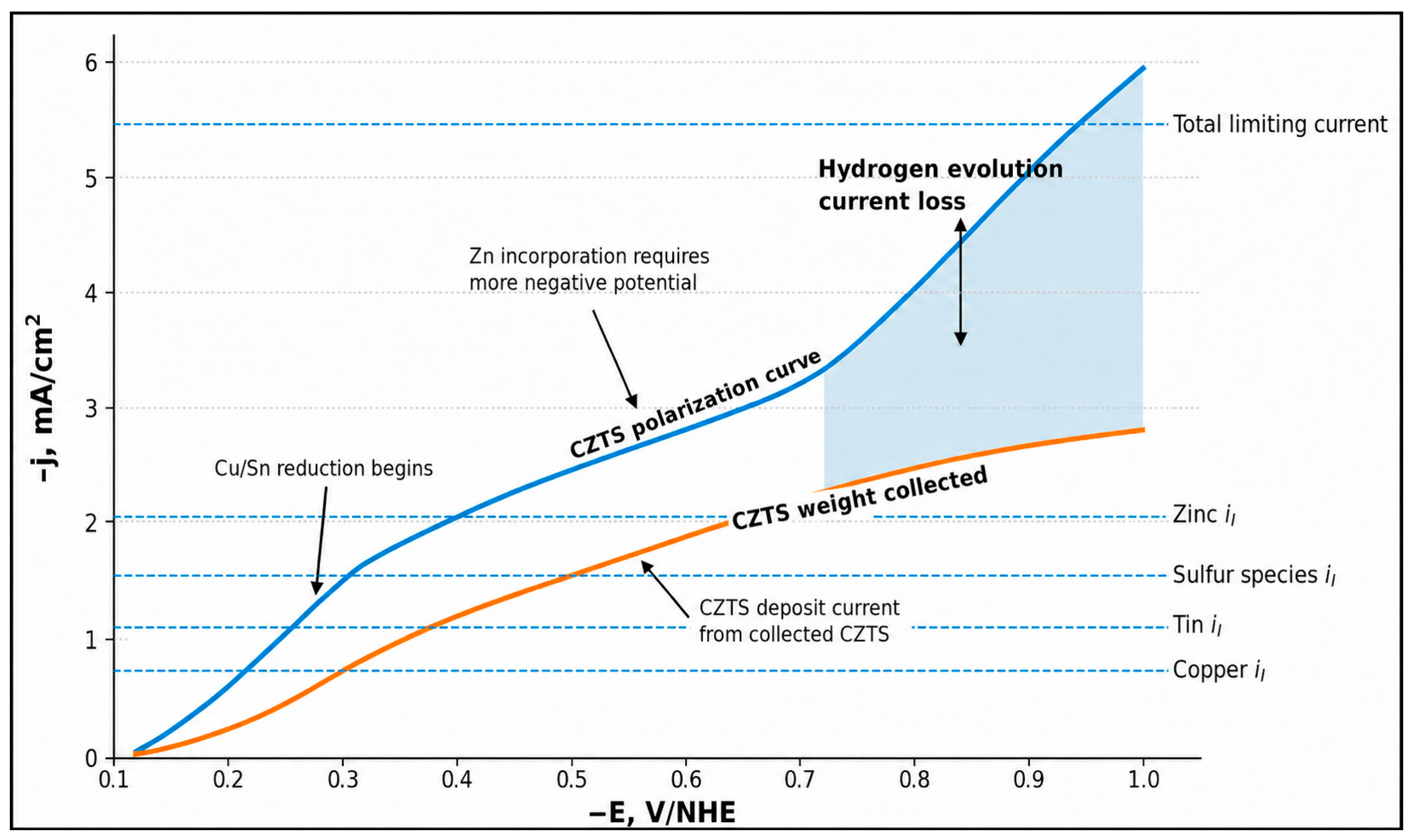
Figure 1 and
Figure 2 are illustrated as hypothetical polarization diagrams to demonstrate the anticipated electrochemical behavior during the electrodeposition of CZTS from a diluted electrolyte. These figures do not constitute direct experimental LSV observations. They are utilized to elucidate the correlation among the total cathodic current, effective deposition current, mass-transfer constraints, and the parasitic current linked to hydrogen evolution. Consequently, characteristics such scan rate, frequency of LSV repetitions, and ohmic-drop correction are irrelevant to these schematic representations. The figures have been reclassified to prevent their representation as experimental polarization curves.
Figure 1 shows the polarization curves for CZTS or Cu–Zn–Sn precursor electrodeposition at varied RDE rotation speeds of 100, 300 and 500 rpm. The proposed electrolyte may contain Cu
2+, Zn
2+, Sn
2+/Sn
4+, and a sulfur source, such as thiosulphate or thiourea, with an appropriate supporting electrolyte and pH control. The curves can be used to examine the impacts of agitation, mass transport, metal ion reduction, sulfur species reactions and hydrogen evolution during CZTS electrodeposition.
Overall, the polarization behavior suggests that the electrodeposition of CZTS is regulated by a combination of charge-transfer kinetics, mass transport, metal ion complexation and hydrogen evolution. Increased RDE rotation speed enhances mass transport and increases deposition current. Excessive cathodic polarization enhances hydrogen evolution and may degrade film quality. The optimal deposition setting should strike a balance between metal co-deposition and hydrogen suppression to form a homogeneous Cu–Zn–Sn precursor with the correct stoichiometry for subsequent sulphurization into the kesterite CZTS absorber layer, as illustrated in
Figure 1.
The use of a pulsed current enables control of the Cu, Zn, Sn, and sulfur species in the final CZTS deposit composition, resulting in a smoother, more uniform precursor layer from the diluted electrolyte solution [
3]. The hydrogen evolution in the usual high-concentration solution occurs more frequently than that in the more diluted electrolytic solution. Moreover, the low concentration of electroactive species promotes the formation of a homogeneous, smooth, and strongly adherent Cu–Zn–Sn precursor deposit, facilitating subsequent sulphurization to obtain the kesterite CZTS absorber layer.
The total deposition current for the diluted electrolyte is, as expected, considerably smaller than that for the high-concentration system, as shown in
Figure 1 [
3]. Furthermore, mass transfer plays a significant role in the electrochemical behavior of Cu, Zn, Sn, and sulfur-containing species in the dilute case, as lower ion concentrations lead to lower limiting currents. This phenomenon is clearly reflected in the polarization curves, in which the deposition current increases with increasing RDE rotation speed. However, at more cathodic potentials, hydrogen evolution becomes more pronounced and competes with the reduction of metal ions, notably when zinc is present. Therefore, the application of pulsed current and dilute electrolyte conditions is vital for controlling composition, improving film uniformity, and reducing excessive hydrogen evolution during CZTS electrodeposition.
3.1.2. Hydrogen Evolution
Figure 2 shows the conceptual relation between the observed CZTS polarization current, the current that contributes to the collected Cu–Zn–Sn/CZTS deposit, the predicted limiting currents of the different species and the current loss due to hydrogen evolution. The total measured cathodic current increases with increasing negative potential demonstrating the progressive reduction of Cu, Sn, Zn and sulphur containing species. However, the current associated with the collected deposit is lower than the total polarization current, especially at higher cathodic potentials. The discrepancy is mainly due to the evolution of hydrogen gas, which consumes part of the applied current and does not participate in the growth of CZTS films. At lower cathodic potentials the rise of the current is mainly attributable to the reduction of copper and tin species. Copper has a better reduction behavior and can deposit earlier than zinc. The involvement of tin species in the early stage of deposition also depends on the electrolyte chemistry, pH, and complexing agents. In this possible region, the contribution from hydrogen evolution is relatively small, and the deposit may be Cu- or Sn-rich if the potential is not low enough to incorporate zinc.
At intermediate potentials, the deposition current approaches the sum of the limiting currents of Cu, Sn, and sulfur species. The region can be considered the co-deposition window for forming a Cu–Zn–Sn precursor suitable for further sulphurization. The circulation passing through the deposit increases steadily, which means better integration of the metallic species. However, careful regulation of the potential is still needed because the final CZTS composition is greatly influenced by the relative reduction rates of Cu, Zn, Sn, and sulfur species. At more negative potentials, zinc inclusion becomes more favorable, as Zn reduction requires a more cathodic potential. However, this prospective zone is also in considerable overlap with hydrogen evolution. Thus, the rise of the total polarization current at high cathodic potentials is not entirely representative of beneficial CZTS deposition. The difference between the overall polarization curve and the curve for the current on the deposit is a large fraction of the current used for hydrogen evolution. Hydrogen evolution may also cause gas bubbles to form on the cathode surface, obstruct active deposition sites, disrupt the local pH, and impair the adherence and homogeneity of deposits.
The comparison between the total limiting current and the measured polarization current reveals that the system cannot be described by metal ion reduction alone. The excess current is primarily due to hydrogen evolution, as the measured current exceeds that expected for the deposition of Cu, Zn, Sn, and sulfur species. This shows that excessive cathodic polarization reduces the current efficiency of CZTS electrodeposition. So, the optimal deposition setting should be selected before hydrogen evolution becomes dominant.
The partial currents data were integrated to give the total current density of CZTS deposition determined from the compositional analysis of the deposit as shown in
Figure 2. The measured total current density differs from the derived one based on the study of the compositional deposit due to the hydrogen evolution.
Figure 2 shows the theoretical limiting current densities, iL, determined from the Levich equation given below [
5],
The limiting current density on a revolving disc electrode in steady-state circumstances is represented by Equation (1). Here, ω stands for the angular rotation rate (rad/s), υ for the electrolyte’s kinematic viscosity (about 0.01 cm
2/s), and A for the working electrode’s geometric axial area. About 35% of the total current in this system comes from the amount of developed hydrogen. This suggests that, when these species compete for reduction at the electrode surface, the concentrations of metal ions and hydrogen evolution may affect the shape of the surface deposit. Where F is the Faraday constant (96,485 C mol
−1), Dj is the diffusion coefficient, ω is the angular rotation rate of the spinning disc electrode (rad s
−1), v is the kinematic viscosity of the electrolyte and Cb,j is the bulk concentration of species j. The angular velocity was found from the rotation speed N by:
For the RDE experiments at 500 rpm:
The practical deposition current density was then determined from the total of the partial limiting currents estimated for the Cu-, Zn-, Sn-, and sulfur-containing species, which was supported by the composition of the produced deposit:
The hydrogen-evolution current density was obtained by subtracting from the measured total cathodic current density the computed practical deposition current density:
The percentage of the current used in calculating hydrogen evolution was consequently computed as:
From the results obtained from
Figure 2 at the specified deposition setting, the measured total cathodic current density was around 8.2 mA cm
−2, and the usable CZTS deposition current density was about 5.3 mA cm
−2. Consequently:
This calculation reveals that roughly 35% of the measured cathodic current is not utilized for effective CZTS deposition and is predominantly expended on parasitic hydrogen evolution. The hydrogen evolution reaction competes with metal ion reduction, diminishes current efficiency, disrupts the local pH at the cathode surface, and may produce bubbles that obstruct active deposition sites.
3.2. Electrodeposition of CZTS Film
The cathodic current density was pulsed with 50 ms on and 50 ms off periods to electrodeposit the CZTS precursor thin films at a current density of 5.3 mA/cm2. The deposition tests were performed at room temperature (approximately 20 °C) for 55 min. The concentrations of Cu, Zn, Sn, and S precursor species in the diluted electrolyte were adjusted to achieve the desired final atomic composition of the CZTS absorber layer. The elemental composition of the deposited films was studied using energy-dispersive X-ray spectroscopy (EDS).
Achieving the required sulfur content and maintaining the correct Cu/(Zn + Sn) and Zn/Sn ratios are key challenges in the electrodeposition of CZTS, especially at low pulsed-current densities. Off-stoichiometric films and possible secondary-phase formation may occur at current densities <~2.9 mA/cm
2 if sulfur species are not sufficiently incorporated into the final film. With no discernible large-scale segregation or depletion zones, the EDS elemental maps in
Figure 3 demonstrate a comparatively uniform lateral distribution of the four constituent elements—Cu, Zn, Sn, and S—across the examined region. To promote crystallization and the formation of the kesterite CZTS phase, the precursor films were annealed for 45 min at 550 °C in argon after electrodeposition. Following annealing, large grains were observed, as shown in
Figure 3. These could be connected to the development of metal sulfide phases or regionally enriched CZTS grains.
A field-emission scanning electron microscope (FE-SEM, [instrument model, manufacturer]) operating at an accelerating voltage of 10–15 kV, a working distance of 7–10 mm, and a beam current of 1–2 nA was used to characterize the surface and cross-sectional morphologies of the CZTS thin films. Images with magnifications between 5000 and 50,000 were primarily captured in secondary electron (SE) mode under high-vacuum conditions. The surface compactness, grain morphology, film continuity, and the existence of microcracks, pinholes, or porous areas were all assessed using these SEM findings.
An energy-dispersive X-ray spectroscopy (EDS) system ([detector model, manufacturer]) coupled with the SEM was used for elemental analysis and compositional mapping. EDS spectra and elemental maps were obtained at a take-off angle of roughly 35°, an acquisition period of 30–50 s, and an accelerating voltage of 15–20 kV. With a pixel dwell time of 50–100 μs, the typical surface-mapping area was 50 × 50 μm2. The presented compositions are average values derived from several measurement points, and quantification was performed using a standardless ZAF correction approach.
During the formation of CZTS films, pulsed-current electrodeposition offers better control over ion transport and nucleation. While the pulse-off time permits the replenishment of depleted ions near the cathode and reduces concentration polarization, the pulse-on period decreases or incorporates Cu-, Zn-, Sn-, and sulfur-containing species at the electrode surface. Additionally, excessive hydrogen evolution, a major problem in aqueous electrodeposition that can result in rough surfaces, pinholes, and poor adhesion, is suppressed during this relaxation period. To create dense, uniform, and nearly stoichiometric CZTS absorber layers suitable for photovoltaic applications, it is crucial to optimize the current density and pulse timing.
The variations in the electrolyte bath composition and their influence on the final atomic composition of the CZTS thin films after annealing in an argon environment are presented in
Table 1. The composition of the bath was altered by varying the quantities of copper sulfate (CuSO
4), zinc sulfate (ZnSO
4), tin chloride (SnCl
2), and sodium thiosulfate (Na
2S
2O
3) as the sources of Cu, Zn, Sn, and S, respectively. These adjustments were made to achieve a final film composition close to the desired stoichiometric ratio for CZTS absorber layers. Pulsed-current electrodeposition was performed at a current density of 5.5 mA/cm
2 utilizing a pulse sequence of 50 ms on-time and 50 ms off-time. The application of pulsed current is vital in CZTS electrodeposition because it enables better control of ion reduction, minimizes concentration polarization near the cathode surface, and helps restrict hydrogen evolution during deposition. During the pulse-on time, the Cu, Zn, Sn, and sulfur-containing species are reduced or incorporated into the film, and during the pulse-off time, the electrolyte near the electrode surface is refilled. This results in a more uniform film and better control over the final composition.
Electrolyte compositions of three deposition baths are presented in the first four columns of
Table 1. The other columns represent the final atomic percentages of Cu, Zn, Sn, and S in the CZTS films after annealing. The results demonstrate that small changes in the bath concentration have a significant influence on the final element’s composition. The last coatings prepared in the examined baths had Cu values (atomic ratio%) of 24.1–24.9, Zn contents of 12.1–12.6, Sn levels of 12.6–13.9, and sulphur contents of ca 49.9–50.1. These numbers are consistent with the expected CZTS composition and suggest that the dilute electrolyte and pulsed-current deposition conditions successfully controlled the incorporation of the four constituent elements. The best-balanced CZTS composition (atomic ratio%) was obtained in bath 3, with 24.9 Cu, 12.6 Zn, 12.6 Sn, and 49.9 S. The stoichiometry is similar to the optimal atomic distribution of Cu2ZnSnS4 with Cu ~25, Zn ~12.5, Sn ~12.5, and S ~50 atomic ratio%. Hence, Bath 3 can be chosen as the most suitable electrolyte formulation among the examined conditions. The near-stoichiometric composition indicates that the chosen pulsed-current settings promoted more uniform deposition and avoided oversaturation or undersaturation of specific species.
The results indicate that, in general, by carefully tuning the composition of the diluted electrolyte and using pulsed-current electrodeposition, CZTS thin films with controlled elemental composition can be produced effectively. The 50 ms on/off pulse sequence provides sufficient relaxation time for ion redistribution in the vicinity of the cathode, leading to improved compositional homogeneity and deposit quality. This highlights the importance of optimizing electrolyte chemistry and pulse timing in manufacturing high-quality CZTS absorber layers for thin-film photovoltaic applications. The residual oxygen concentration was extremely low and was primarily attributed to surface oxidation rather than bulk assimilation into the CZTS coating.
3.3. Grain Size and Morphology
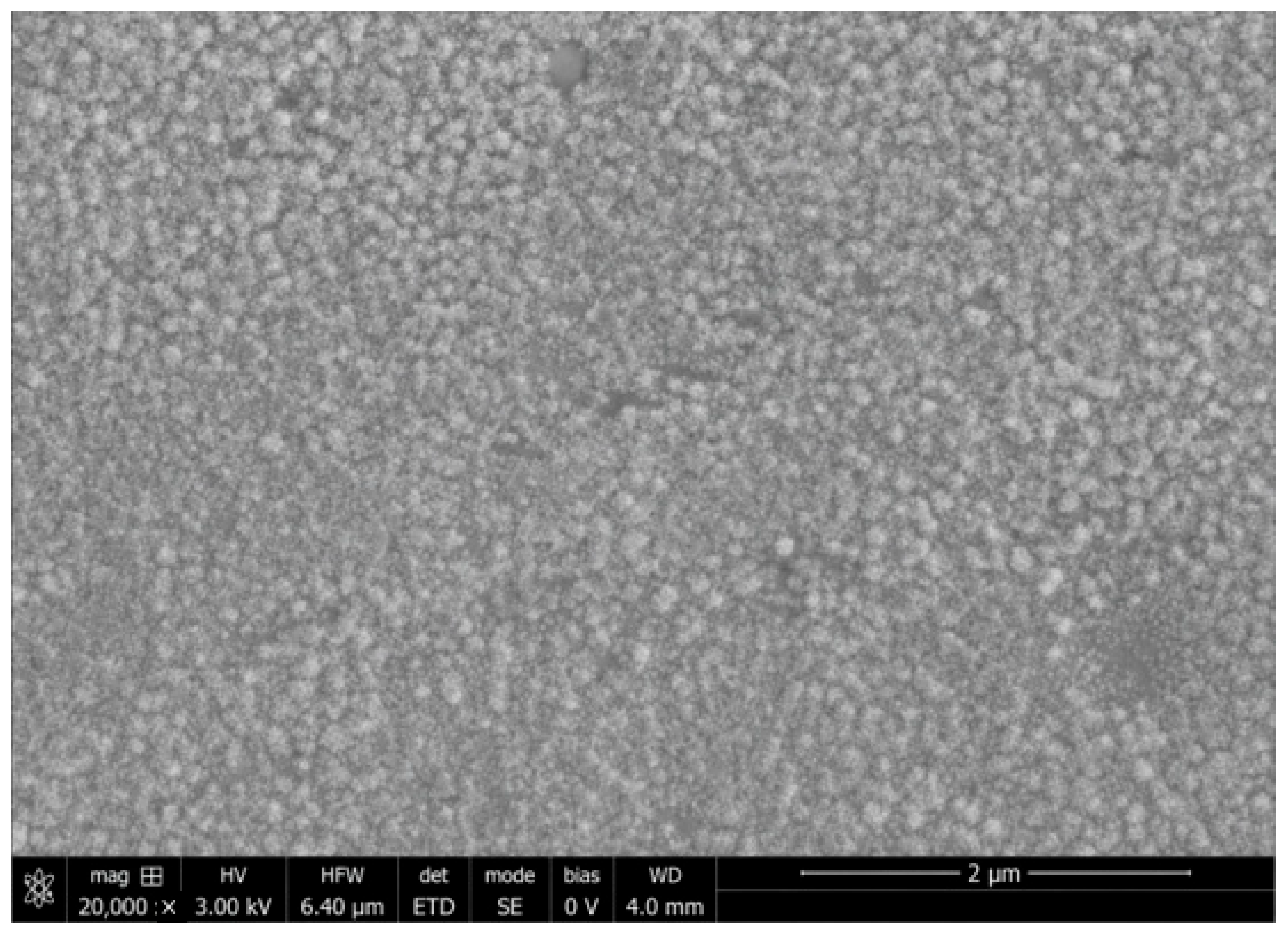
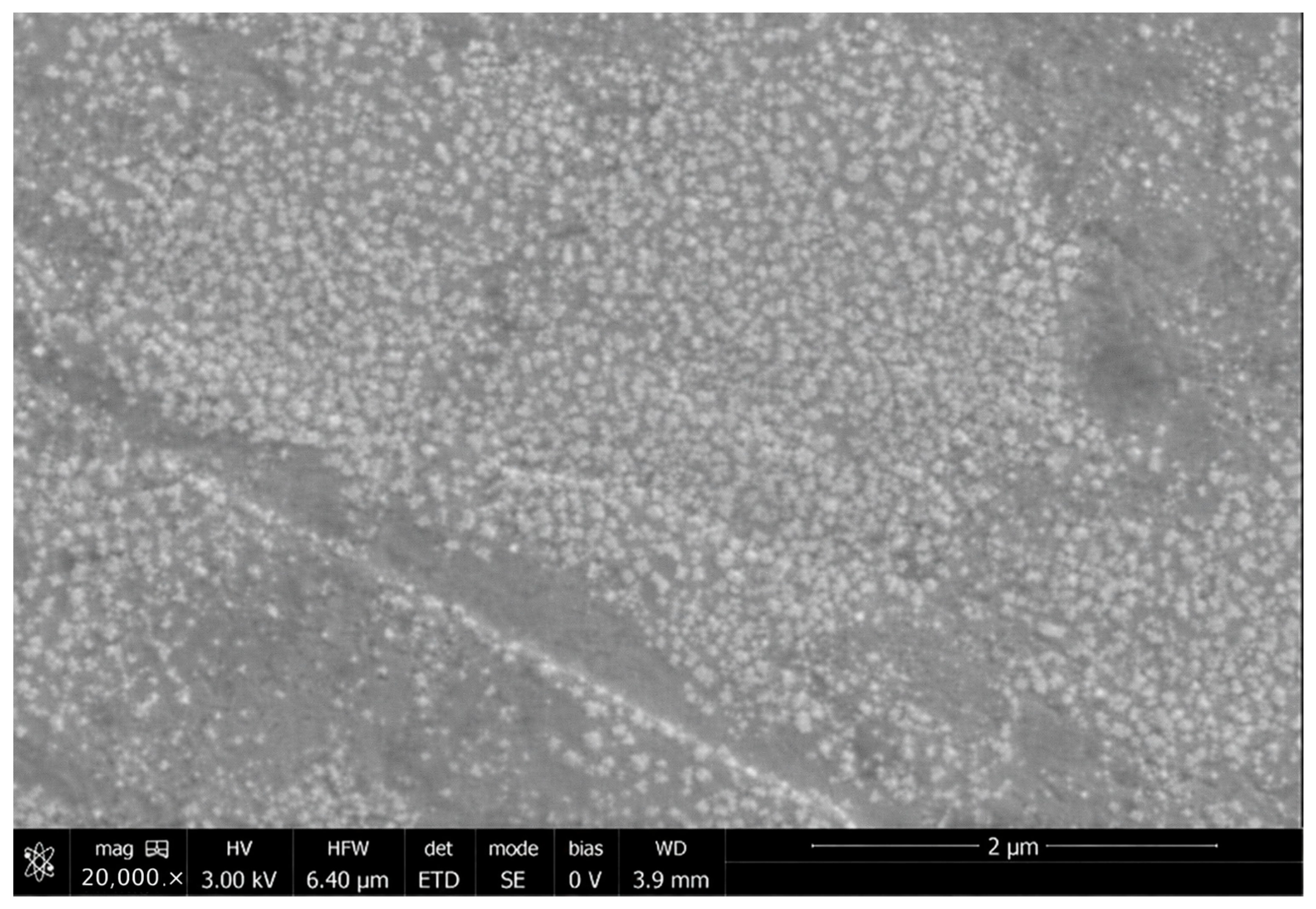
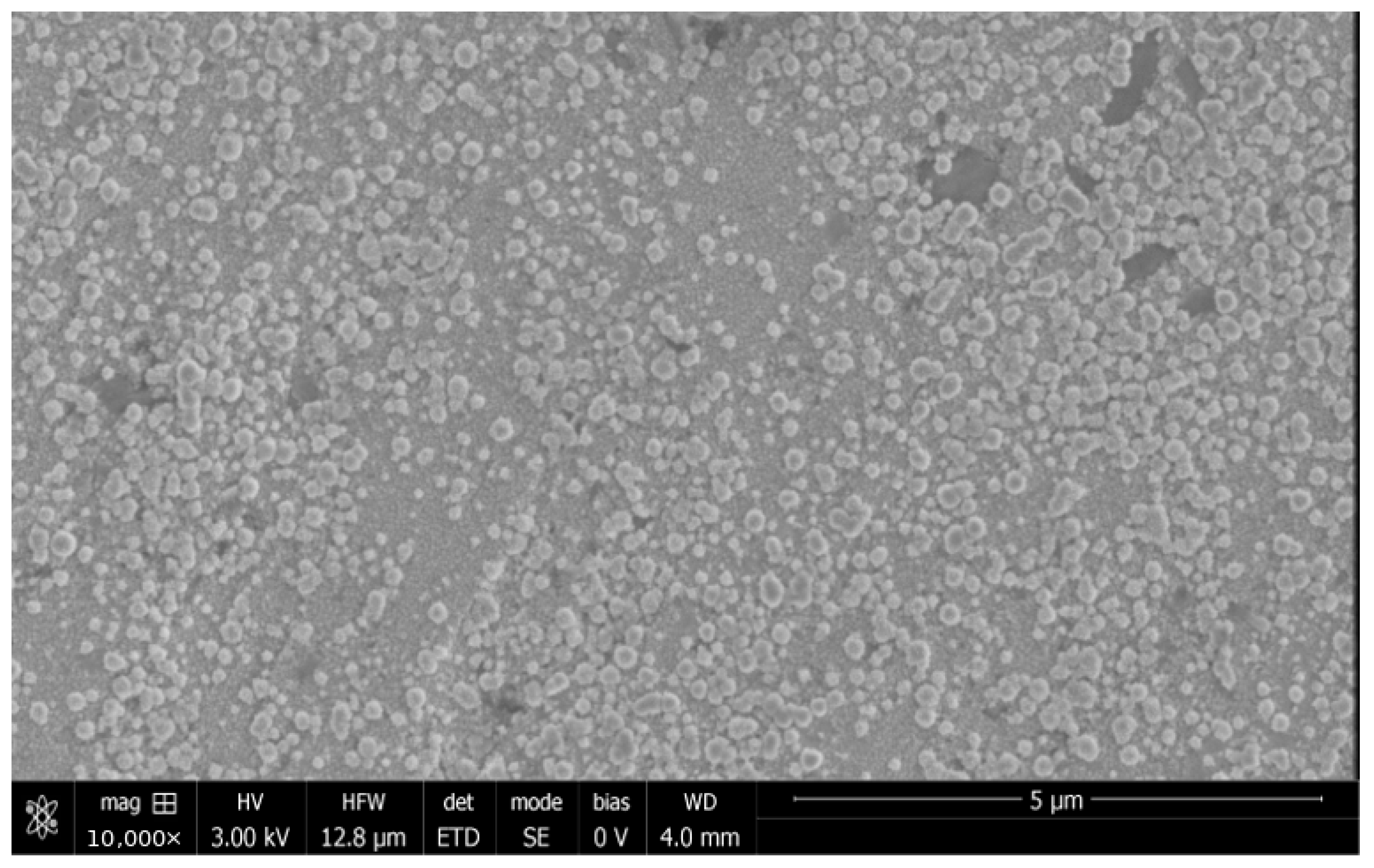
Three CZTS samples, produced under varying pulsed current densities and timing conditions, were analyzed to assess the impact of the pulsing approach on the morphology of the absorber layer. The SEM image indicates that the pulsed electrodeposition parameters significantly affect the surface texture, grain distribution, and density of the deposited CZTS layer. The initial sample deposited at 5.5 mA/cm
2 with 50 ms on-time and 50 ms off-time displays a rather homogeneous distribution of fine grains across the substrate. The short-pulse deposition condition yielded a relatively smooth and dense CZTS layer. The SEM micrograph reveals that the deposit consists of small, densely packed grains, with an estimated grain size in the sub-micrometer range. The brief off-time facilitates partial replenishment of Cu
2+, Zn
2+, Sn
2+/Sn
4+, and sulfur-containing species adjacent to the electrode surface, whereas the brief on-time mitigates excessive local concentration depletion and curtails the development of roughness. The deposited CZTS film exhibits enhanced surface coverage and a more uniform shape (
Figure 4).
In pulsed-current electrodeposition, the on-time facilitates the reduction and nucleation of metallic or chalcogenide precursor species, whilst the off-time aids in the transport of ions from the bulk electrolyte to the electrode surface. Consequently, short-pulse conditions can increase nucleation density and limit uncontrolled grain coarsening. This elucidates the detailed CZTS morphology depicted in the SEM image. The uniform distribution of grains suggests that pulsed current promotes compositional and morphological uniformity in electrodeposited CZTS absorber layers, as illustrated in
Figure 4. However, in other parts of the image, variations in contrast and less-dense patches may indicate non-uniform local deposition, partial agglomeration, or different surface development rates. These characteristics are generally related to the simultaneous electrodeposition of several elements in CZTS, because of the different reduction behaviors and mass-transfer qualities of Cu, Zn, Sn, and S. The grains were fine, compact, and well distributed. The mean grain size was about 280 ± 45 nm, and most of the grains were scattered between 210 and 360 nm. This demonstrates that the short-pulse condition favors regulated nucleation and avoids excessive grain coarsening. This is due to reasonable ion replenishment during off-time and restricted local ion depletion during on-time, resulting in a compact and uniform grain distribution. Thorough adjustment of current density, pulse duration, electrolyte composition, and pH is crucial to get a thick, crack-free, and homogeneous CZTS precursor film suitable for absorber-layer formation after sulfurization (
Figure 4).
The CZTS sample electrodeposited at a pulsed current density of 5.4 mA/cm
2, with 100 ms on-time and 100 ms off-time, under similar deposition conditions, is shown in
Figure 5. A rougher surface morphology was observed compared to the preceding short-pulse sample due to the longer pulse length and increased current density. The longer the on-time, the greater the local consumption of Cu, Zn, Sn, and sulfur-containing species around the electrode surface, which causes this behavior. This results in stronger concentration gradients, less homogeneous nucleation, and increased grain development.
SEM inspection reveals that the CZTS deposit continues to cover the substrate surface, but the grain distribution is less homogeneous than that achieved with shorter pulse periods. The increase in current density may also result in quicker deposition and localized growth, leading to bigger crystallites and a rougher film texture. This phenomenon is crucial in the electrodeposition of CZTS, as the four constituent species exhibit varied reduction kinetics and different mass-transfer behavior. Thus, longer pulsing conditions can be less favorable for compositional uniformity if the off-time is insufficient to fully replenish the depleted ions at the electrode–electrolyte interface.
The film formed with less than 100 ms of on/off pulsing has satisfactory surface coverage; nonetheless, its rougher morphology suggests that longer pulse durations and higher current densities can promote agglomeration and non-uniform development. Such morphology may influence the subsequent sulphurization phase, grain coalescence, and absorber-layer quality. The medium-pulse sample, deposited with 100 ms on-time and 100 ms off-time, exhibited an average grain size of 430 ± 80 nm, with a distribution ranging from 300 to 600 nm. The augmentation in particle size and dispersion breadth signifies a reduction in uniformity of growth relative to the short-pulse sample. This is ascribed to heightened concentration polarization during the extended pulse-on duration. Thus, optimal control of pulsed current density and timing is necessary to generate compact, homogeneous, and crack-free CZTS films for thin-film solar cell applications.
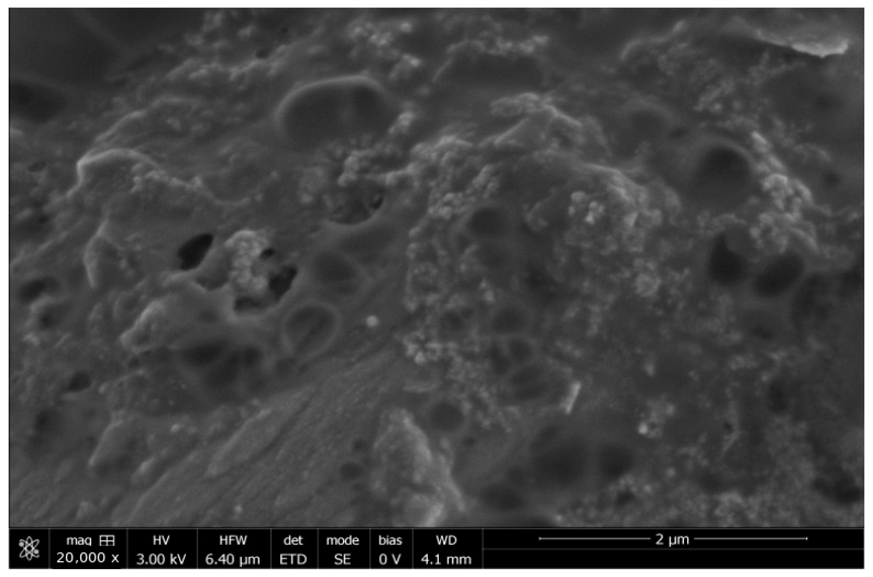
The third CZTS sample (
Figure 6) electrodeposited at a pulsed-current density of 5.9 mA/cm
2 with a longer pulse duration of 250 ms on-time and 250 ms off-time at similar deposition conditions is shown in
Figure 6. This sample has a much rougher and coarse surface morphology than the preceding samples produced at shorter pulse periods. Prolonged on-time allows more material to be deposited per pulse, which may lead to increased local ion depletion near the electrode surface and encourage non-uniform development. SEM observation shows that the CZTS deposit covers the surface of substrate, but the grain distribution is worse and less homogenous than that of the short-pulse samples. The long pulse length might decrease the efficiency of the off-time in restoring the concentration of Cu, Zn, Sn, and sulfur-containing species at the electrode–electrolyte interface. This, in turn, makes local deposition and agglomeration more dominant, leading to larger grains and a coarser surface texture (
Figure 6).
In particular, in the case of CZTS electrodeposition, adjusting the pulse duration is critical due to the variable reduction kinetics and diffusion behavior of Cu, Zn, Sn, and sulfur species. The deposition process is less controlled if the pulse period is too long, which might lead to rough patches, non-uniform composition, or larger crystallite clusters in the film. The long-pulse sample, with 250 ms on-time and 250 ms off-time, exhibited larger and more agglomerated grains. The mean grain size was approximately 650 ± 140 nm, with some agglomerated areas exceeding 850 nm. The extensive grain-size distribution corroborates the irregular growth evident in the SEM image. This phenomenon results from sustained ion depletion near the cathode surface and increased localized growth during the extended pulse-on duration. Consequently, the long-pulse regime is suboptimal for generating compact, uniform CZTS absorber layers.
The sample deposited at 5.4 mA/cm2 with 250 ms on/off still shows continuous surface coverage, but the rougher morphology indicates that this setting is less favorable for a compact and homogeneous CZTS absorber layer.
3.4. Deposit Analysis
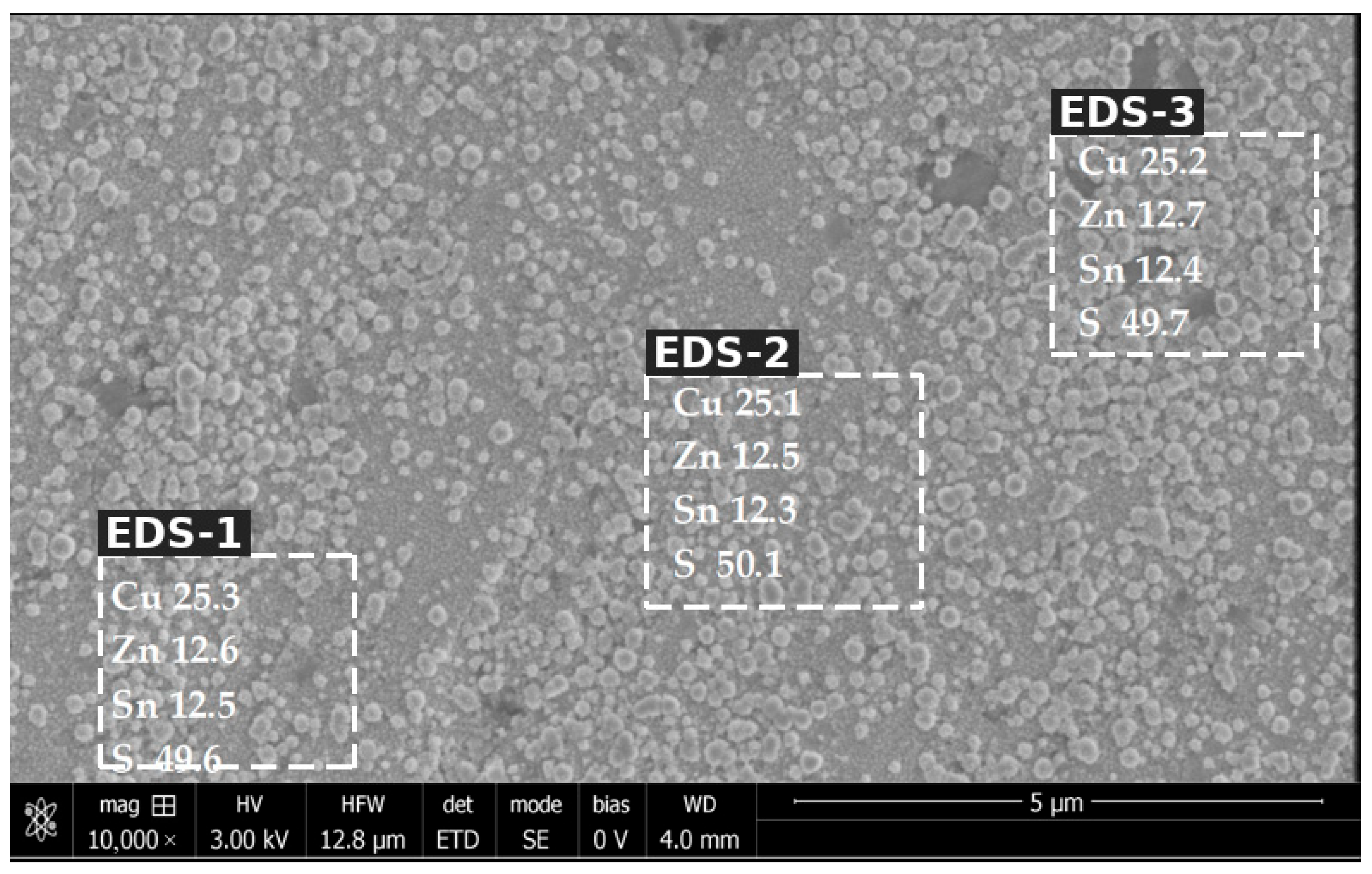
EDS analysis was carried out at several selected positions on the surface of the CZTS absorber layer to assess the lateral elemental distribution produced by pulsed-current electrodeposition. The SEM image in
Figure 7 shows local compositional values and a very uniform elemental distribution across the left, middle, and right sections of the sample. The typical elemental composition (atomic ratio%) was approximately Cu 25.2, Zn 12.6, Sn 12.4, and S 49.8. These values are close to the expected stoichiometric composition of CZTS, indicating that the pulsed-current technique has successfully enabled the co-deposition of Cu, Zn, Sn, and sulfur-containing compounds. The calculated Cu/(Zn + Sn) is about 1.01. The corresponding Zn/Sn is about 1.02. The ratios confirm that the deposited CZTS layer is close to stoichiometry, with a slight Cu-rich bias. The minor fluctuations in composition across the measured locations demonstrate good lateral compositional homogeneity across the film surface. This homogeneity results from the pulsed-current deposition process, in which the on-time favors nucleation and growth, while the off-time partially replenishes ions depleted at the electrode surface. SEM picture also shows a somewhat continuous deposit of CZTS with fine grains dispersed on the surface. Some particle aggregation is also visible, but the composition is essentially consistent across the regions investigated, confirming that the pulsing technique improves elemental distribution during electrodeposition. In general, the results from EDS and SEM confirm that the CZTS films generated by pulsed-current electrodeposition may achieve desirable surface coverage and good compositional uniformity, which are necessary criteria for producing high-quality CZTS absorber layers following sulphurization (
Figure 7).
Final thickness of the CZTS film obtained at the different current densities and pulse timings. The thicknesses of the as-deposited and annealed films were measured by cross-sectional SEM analysis and confirmed by stylus profilometry. The thickness of the CZTS layer was about 1.5 to 1.75 μm, which is predicted to be sufficient to absorb 96% of the incident light.
3.5. Post-Deposition Thermal Annealing
Thermal annealing is a necessary step to optimize the atomic structure of the deposit, to remove recombination defects, and to ensure homogeneous composition across the sample [
37,
38,
39]. The post-treatment conditions were the same as those defined for the CZTS layer in the previous investigation. The reduced annealing time is based on our previously published work [
38], where the annealing process for CZTS layers was systematically studied and optimized, and on a limited set of supplementary experiments in this study, ranging from 1.5 h to 50 min, to optimize the annealing parameters for films from the diluted electrolyte.
Table 2 depicts changes in the deposit composition, evaluated before and after annealing. The atomic composition of the plated CZTS film before and after annealing is shown in
Table 2. All values have been rounded to one decimal place, and the composition values are reported in at.%.
5. Conclusions
In this work, pulsed-current electrodeposition was successfully used to create CZTS thin films from a diluted electrolyte. This work’s innovation is the integration of a low-metal ion-concentration electrolyte with pulsed-current control to enhance ion replenishment, diminish concentration polarization, and restrict parasitic hydrogen evolution during CZTS electrodeposition. The effects of current density and pulse timing on film composition, morphology, crystallinity, and device performance were examined. The findings show that the co-deposition of Cu, Zn, Sn, and sulfur-containing species in a low-concentration solution may be effectively controlled using the pulsed-current technique. One of the primary drawbacks of aqueous CZTS electrodeposition is excessive hydrogen evolution. According to the current-balance analysis using the Levich-limited deposition current and the recorded total cathodic current, it was calculated that roughly 35% of the total current was attributed to hydrogen evolution under the specified deposition conditions. The pulsed-current settings and electrolyte content significantly influenced the final film stoichiometry. With Cu, Zn, Sn, and S contents close to the optimal atomic distribution of Cu2ZnSnS4, the optimized composition among the examined baths yielded a CZTS film with an anticipated stoichiometric ratio. The pulsed-current method produced a relatively uniform elemental distribution across the film surface, as indicated by EDS data. The computed Zn/Sn and Cu/Zn + Sn ratios were near unity, indicating that the cation balance was well controlled under ideal deposition conditions.
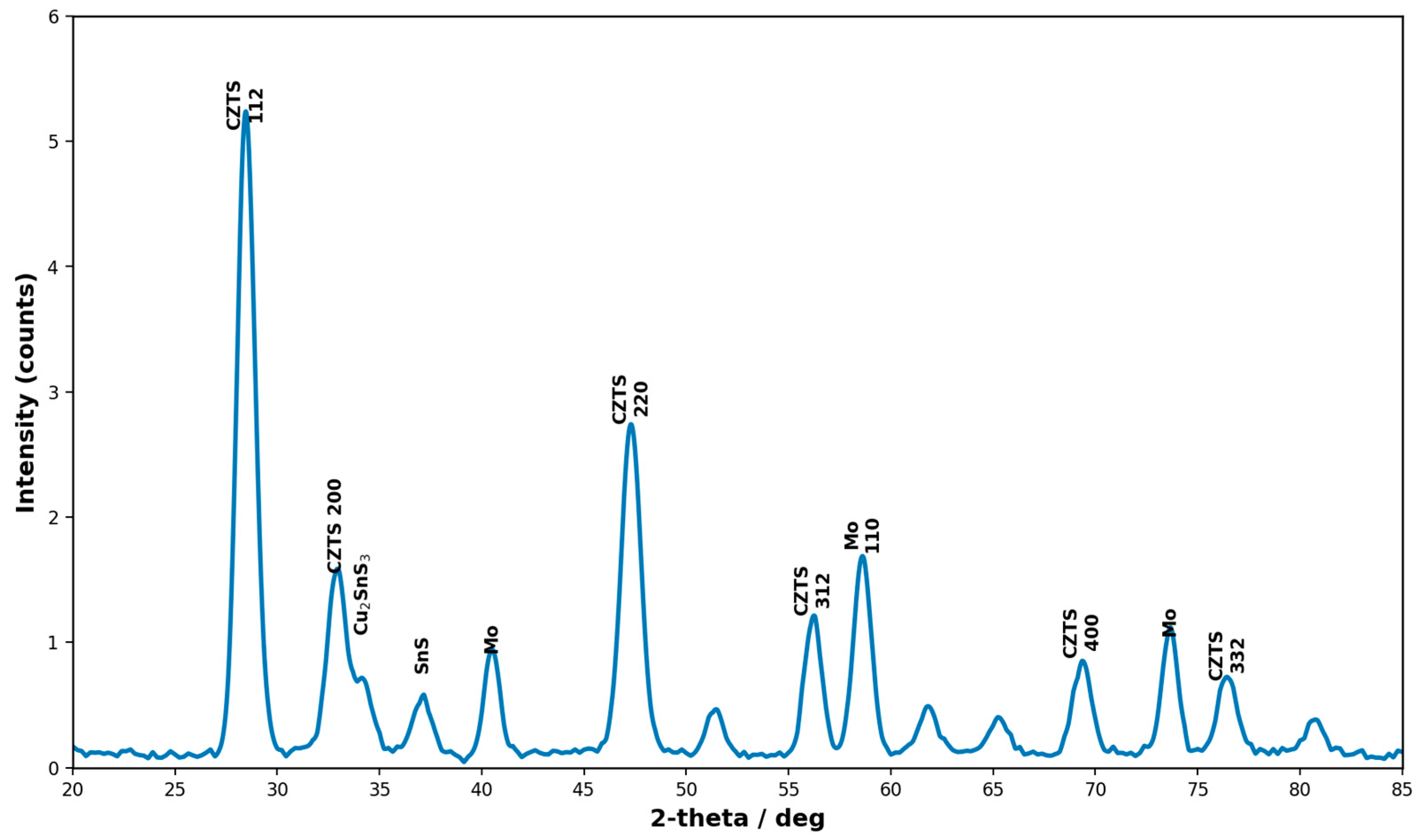
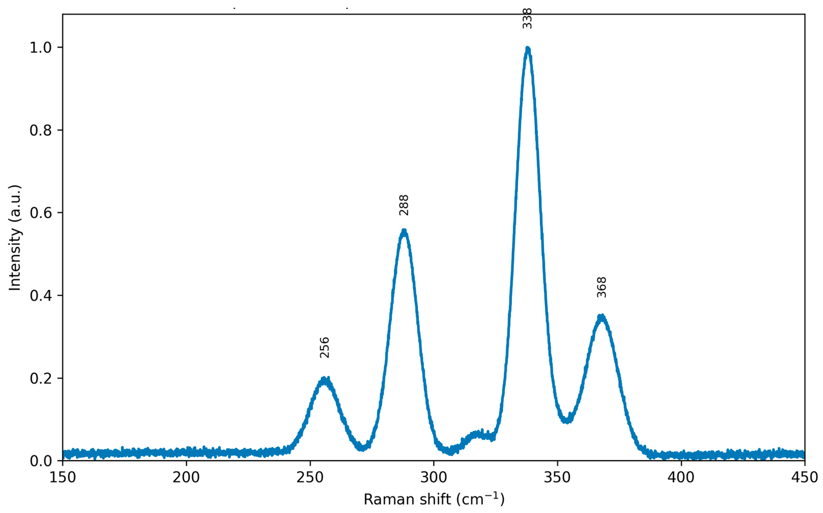
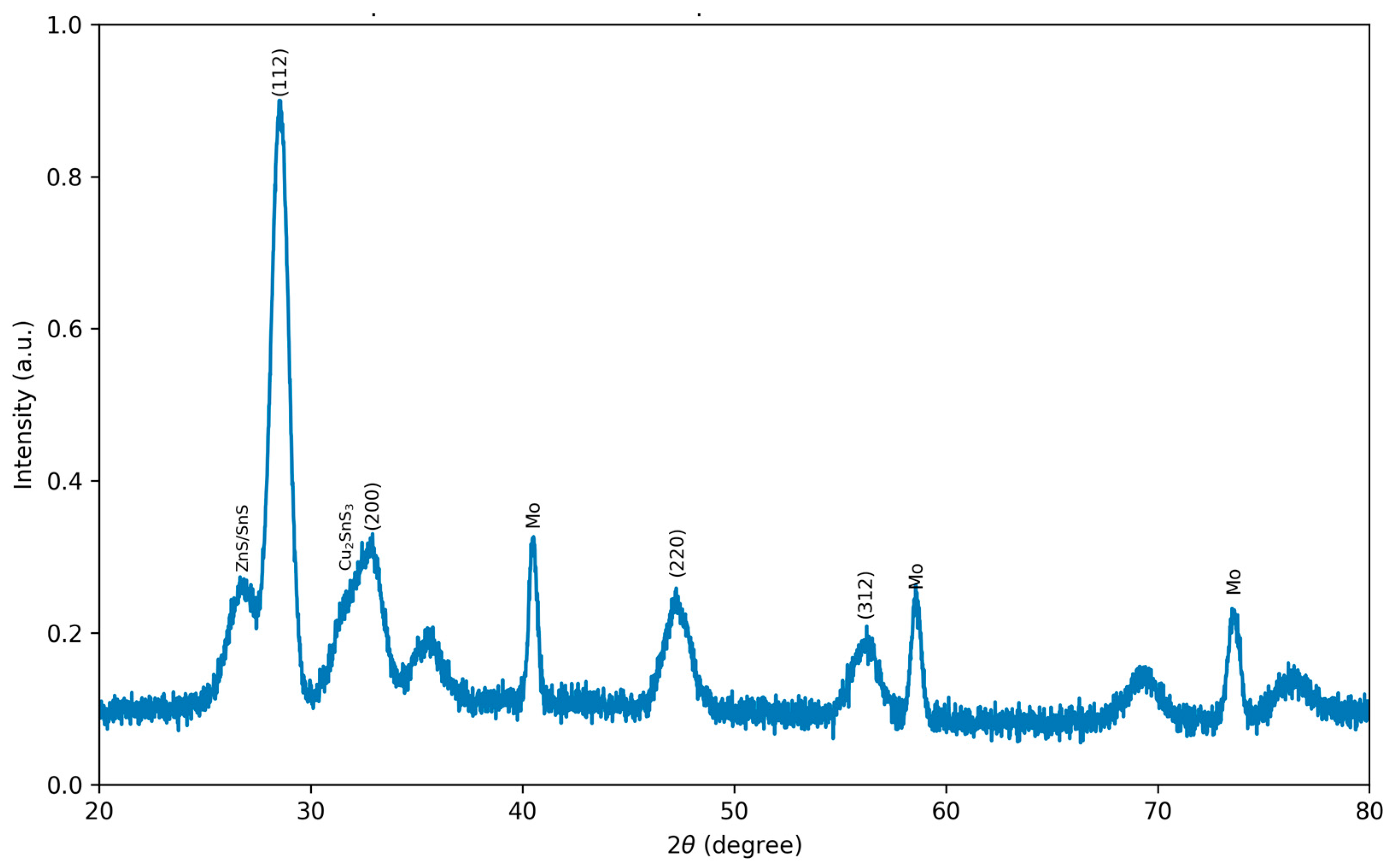
Grain size, compactness, and surface morphology were all significantly impacted by pulse time according to the SEM examination. The short-pulse sample exhibited a smaller and narrower grain-size distribution; in contrast, the 100 ms and 250 ms pulse samples exhibited larger grains, broader grain-size distributions, and more agglomerated surface features, as demonstrated by quantitative SEM image analysis. Stronger local ion depletion during the prolonged on-time and inadequate recovery of ion concentration during the off-time were blamed for this behavior, and, to produce dense and homogeneous CZTS precursor layers, shorter pulse durations were therefore more advantageous. The crystallinity and phase formation of the electrodeposited CZTS films were enhanced by post-deposition annealing. With the major diffraction peak corresponding to the preferred (112) orientation, the XRD data confirmed the formation of the kesterite CZTS phase. The strong CZTS diffraction peaks indicate that the chosen pulsed-current deposition and annealing conditions are appropriate for forming crystalline CZTS absorber layers, although weak secondary phases may still be present. The advantage of using Raman spectroscopy as a supplemental phase-identification approach was also discussed, with characteristic Raman modes at approximately 288, 338, and 368 cm−1 confirming the formation of the dominant kesterite CZTS phase and improving phase discrimination relative to XRD analysis. Films made via pulsed-current electrodeposition from diluted electrolytes can serve as absorber layers in thin-film solar devices, as demonstrated by the satisfactory photovoltaic performance of the manufactured CZTS solar cells. The short-pulse condition yielded the highest device performance, with increased photovoltaic response resulting from improved film compactness, greater compositional uniformity, and reduced roughness. While the drop at longer wavelengths indicated that recombination losses, limited carrier diffusion length, and absorber-layer flaws still limit device performance, the quantum-efficiency measurements demonstrated strong photon absorption in the visible area.
In conclusion, our study demonstrates that diluted-electrolyte pulsed-current electrodeposition is a viable, affordable, and scalable method for creating CZTS absorber layers. The production of functional CZTS solar-cell devices was aided by the optimized short-pulse deposition condition, which also preserved near-stoichiometric composition and enhanced film shape. Further developments should result from more exact control over hydrogen evolution, electrolyte chemistry, pulse parameters, interface engineering, and post-deposition sulphurization. These developments could contribute to the evolution of ecologically safe and abundant CZTS thin-film solar cell technology.