Abstract
Microfluidic devices are used in numerous scientific fields and research areas, but device fabrication is still a time- and resource-intensive process largely confined to the cleanroom or a similarly well-equipped laboratory. This paper presents a method to create microfluidic devices in under three hours using the silicone polymer polydimethylsiloxane (PDMS) and a laser cut positive master using PDMS double casting without a cleanroom or other large capital equipment. This method can be utilized by an undergraduate student with minimal training in a laboratory with a modest budget. This paper presents “Same Day Microfluidics” as a fabrication method accessible to research groups not currently fabricating their own microfluidic devices and as an option for established research groups to more quickly create prototype devices. The method is described in detail with timing, materials, and technical considerations for each step and demonstrated in the context of a Y-channel coflow device.
1. Introduction
Since their initial development in the 1990’s, microfluidics has become nearly ubiquitous in many academic fields [1]. The original manufacturing process for microfluidic devices, soft lithography [2,3], creates surface relief on a silicon wafer via photolithography [4] and then casts the silicone polymer polydimethylsiloxane (PDMS) onto the wafer to invert the features. In soft lithography the surface relief of the cured photoresist is the inverse of the final device and is called a “negative master” following from the terminology of developing photographic negatives. However, when creating the initial master via a method other than photolithography, such as plasma etching [5], laser ablation [6,7,8], razor writing [9,10,11], micromilling [12,13,14], or wet etching [15], it is often preferable to create a “positive master” with surface relief which matches the final device. The use of these alternative technologies for microfluidic fabrication is increasing dramatically due to the reduced cost and fabrication time compared to traditional photolithography. These new technologies have greatly expanded access to microfluidics such that their fabrication has moved from the cleanroom into MakerSpaces [16].
Creating a microfluidic device from a positive master requires a two-stage casting process. An intermediate negative master must first be cast from the original positive master, and then this intermediate negative master can be used for casting final PDMS devices. Due to the difficulty of separating PDMS layers several technologies have been developed to create intermediate masters out of polymethylmethacrylate (PMMA) sheets via thermal imprinting for mass production [17] or casting polyurethane resin [18] or epoxy resin [19] for rapid prototyping. A preferable method, PDMS “double casting” where the intermediate master is also PDMS, requires careful separation of the PDMS layers [20]. This separation is a known challenge due to the presences of uncured PDMS remnants [21]. To prevent bonding between PDMS layers, typically either a release agent is applied to the intermediate or the intermediate is chemically passivated [22,23]. Numerous release agents have been used including hydroxypropylmethylcellulose (HPMC) [22,24], ceramic surfactants [25], silicone oil [8], and silanization with either tetraethylorthosilicate [26] or perfluorodecyltrichlorosilane [27,28]. Chemical passivation has been explored using thermal aging [21,29,30,31] and plasma/alcohol treatment [32,33]. Investigations into PDMS double casting methods is ongoing with recent work looking into creating separable layers by augmenting the curing ratio and temperature of the PDMS layers [34].
Despite the proliferation of alternative technologies and numerous investigations into faster fabrication methods, soft lithography remains the gold standard for microfluidic devices. This paper introduces “Same Day Microfluidics” as a fast, inexpensive, and readily accessible fabrication method for the production of microfluidic devices. The method presented here is faster and less expensive than traditional soft lithography, uses no toxic or hazardous compounds in the PDMS double casting, and does not require any delicate physical manipulations in the fabrication procedure. This method utilizes a readily accessible 20 W laser cutter to pattern the surface relief of a microfluidic channel into a substrate consisting of multiple layers of polyimide tape over a layer of aluminum tape on a piece of microscope glass. PDMS double casting is then used to create functional devices as replicas of the patterned master. An initial PDMS cast is used to clean the master of laser ablation debris and to image the channel profile, a second PDMS cast creates a negative master with the inverse surface relief, the negative master is chemically passivated to allow for direct PDMS-PDMS casting, and a final PDMS cast creates the positive surface relief of the functional device. This method allows for going from a computer design to a functional microfluidic device in under three hours.
2. Materials and Methods
The Same Day Microfluidics method consists of substrate preparation, device design, positive master creation and cleaning, negative master casting and passivation, and final device casting and finishing. This section describes the equipment and materials used along with a thorough description of each step of the process.
2.1. Materials
The substrate was prepared from layers of polyimide “Kapton” tape (Hxtape Hx-JSZ) with a layer of aluminum tape (PowerScale A150) to block the cutting laser over a glass microscope slide for rigidity and durability. For this paper, devices were designed in Fusion 360; however, any CAD software should work. A Snapmaker A350 (Shenzhen, China) with a 20 W laser module was used to create the positive master, and Snapmaker Luban was used to create the CNC g-code from the CAD design. The PDMS (Qsil 216) was prepared with a planetary centrifuge (Thinky ARE-310, Tokyo, Japan) for mixing and defoaming, degassed in a vacuum chamber, and the bubbles were removed with a heat gun. To cure the PDMS, a glass petri dish was used as a container in a laboratory oven (Cole-Parmer Gravity Convenction Drying Oven, Vernon Hills, IL, USA). To enable double-casting of PDMS, methanol, a plasma chamber (Diener Zepto One, Ebhausen, Germany), and a vacuum chamber were used. Devices were finished by punching access holes (WellTech Rapid-Core 0.75, Katy, Texas, USA) and plasma bonding to a glass microscope slide.
Note that PDMS can be prepared manually without a planetary centrifuge by stirring the two components together and defoaming the mixture in a vacuum chamber. Manually preparing PDMS takes significantly longer, but not having access to a planetary centrifuge does not prevent the usage of this method.
2.2. Substrate Preparation
The first step for this method is substrate preparation. Aluminum and polyimide tape are layered upon a glass backing, a full 50 mm by 75 mm microscope slide was too large to fit into the petri dishes available so they were cut down to 50 mm by 50 mm squares. To start, a layer of aluminum tape from a 2 in (50 mm) wide roll is placed onto the piece of glass taking great care to minimize the air bubbles to ensure uniformity across the whole plane of the tape. It is crucial that air bubbles are minimized not only in number but in size since any air bubble’s features will propagate through the preparation of the sample with each subsequent layer of polyimide tape. Utilizing a straight object with a very fine edge, such as a razor blade, is useful when laying down the tape layers. We found the best results by starting at one edge of the glass plane, holding the tape taught, and then slowly working to the other edge of the plane using a razor blade to ensure no air bubbles would be trapped. The aluminum tape used here is nominally 3.9 mil (99 μm) thick but was measured with an optical micrometer as 88 μm. After the layer of aluminum tape the ablation substrate is built up from layers of polyimide tape from a 2 in (50 mm)-wide roll with the same precautions to ensure air bubble and contaminant minimization. The depth of the final microfluidic channel is set by the number of layers of polyimide tape used. The polyimide tape used here is nominally 1 mil (25.4 μm) of polyimide with an additional 1.4 mil (35.6 μm) of silicone adhesive. Using an optical micrometer we measured the thickness of a single layer of polyimide tape applied to aluminum tape as 30 μm from the aluminum. For this paper we used five layers of polyimide tape to create channels 158–233 μm deep. The variability in channel depth is likely due to variations in the adhesive layers from roll removal and application. Substrate thickness variation is mostly between technicians with minimal variation between different substrates made by the same technician. With practice consistent substrates can be prepared in about 10 min. Preparing the substrate is shown in Figure 1.
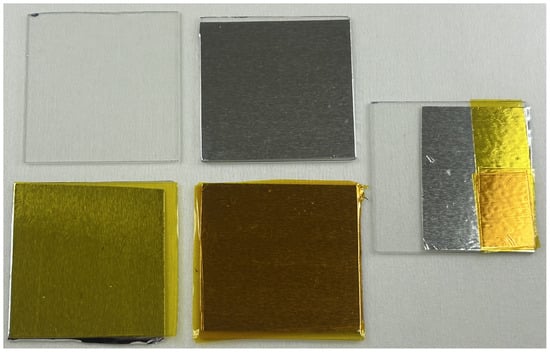
Figure 1.
The process of substrate preparation starting from a cut glass backing slide (top left), with a layer of aluminum tape (top middle), with a single layer of polyimide tape (bottom left), and with five layers of polyimide tape (bottom middle). On the right is a test piece for depth measurements with bare glass, aluminum tape, a single layer of polyimide tape, and five layers of polyimide tape. Using an optical micrometer the various thicknesses were measured as 88 μm for the aluminum tape from the bare glass, 30 μm for a single layer of polyimide from the aluminum, and 158 μm for five layers of polyimide from the aluminum.
2.3. Device Design
To demonstrate the method in this paper, we designed a Y-channel coflow device 300 μm wide. Any planar device can be created using this method, but a multi-layer device would require a more sophisticated fabrication technology. The primary design limitation is the dot size of the laser module; here we used a Snapmaker A350 20 W laser module which is a continuous 450 nm laser with a 80 μm × 100 μm dot size. For this work the design was created in Fusion360 where the channel is designed as a parametric sketch and then exported as a .dxf file. Since we used a Snapmaker laser module, we used Snapmaker Luban to generate the g-code. With practice a channel can be designed and processed in about 15 min. The design of the device is shown in Figure 2.
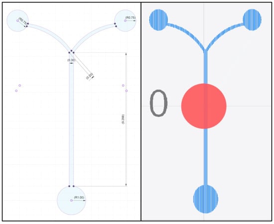
Figure 2.
The Y-channel coflow device design used to demonstrate this method. The sketch in Fusion360 (left) shows the design dimensions for the 300 μm wide channel coflow device, and the beampath in Luban (right) shows the raster pattern the laser will follow during fabrication. The raster pattern has been selected so that the beam path follows the coflow channel.
2.4. Positive Master Creation & Cleaning
To create the positive master via laser ablation, the substrate is mounted in the laser cutter, the g-code for the design is loaded into the laser cutter control unit, and the focus of the cutting laser adjusted to the top of substrate surface. In this work we found that for five layers of polyimide tape a single pass at 25% of the 20 W laser power with 1000 mm/min work speed and 0.04 mm fill interval were optimal. Laser ablation of the positive master takes about 1 min, with up to 5 min of additional time for loading and focusing. The positive master after laser ablation is shown in Figure 3.
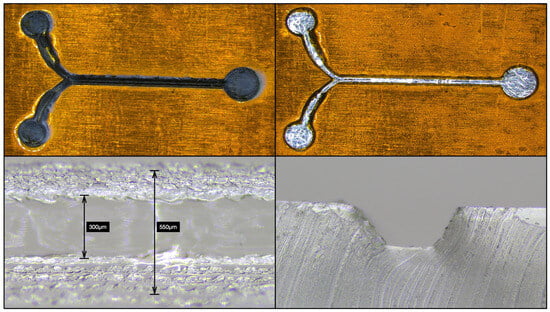
Figure 3.
The positive master after laser ablation, cleaning, channel measurements, and channel profile. The process of laser ablation leaves residue which can be clearly seen (top left), but a round of PDMS casting removes most detritus (top right). A PDMS cast is used to measure the channel width (bottom left) and sliced to image the channel profile (bottom right). The channel width was measured as 300 μm wide at the bottom and 550 μm at the top. The depth of the channel was measured with an optical micrometer as 233 μm. Note that the PDMS cast used for cleaning can also be used to measure the channel width and profile, but the images are typically of lower quality.
After the channel has been patterned onto the substrate, there will most likely be residue which needs to be removed before the intermediate negative master can be cast. To clean the positive master, a thin PDMS cast is used to physically remove the residue. An optional pre-cleaning step can be performed before this with a small object such as a hypodermic needle to loosen and remove some of the charred material before the PDMS casting step; however, care needs to be taken to ensure that the aluminum beneath is not scratched or dented. The PDMS is prepared as 22 g at a 10:1 ratio of monomer to cross-linker mixed and defoamed in the planetary centrifuge, poured over the positive master in a glass petri dish, and degassed in a vacuum chamber for 20 min to remove air bubbles and embed the residue in the PDMS. Surface bubbles are removed with a heat gun and then cured at 150 °C for 4 min. Due to the high curing temperature, the PDMS is allowed to cool for 5 min before continuing. It is worth note that the polyimide tape is rated for long-term exposure to temperatures up to 280 °C and is thus stable for numerous repeat castings while the adhesive for the aluminum tape is rated at 250 °F (121 °C) and should thus be allowed to cool before handling.
After the cured PDMS has cooled, a circle is cut around the features leaving an outer ring (approximately 1 cm wide) to contain the PDMS during the intermediate negative master casting step. The inner circle is removed to pull the residue out of the positive master. The PDMS cast containing the residue can then be sliced and imaged under an inspection microscope to measure the profile of the microfluidic channel. This process takes about 30 min. The positive master after cleaning and the channel profile are shown in Figure 3. From the channel profile you can see that the channel is not perfectly rectangular due to the Gaussian profile of laser ablation [6]. From the channel profile you can also see that the channel floor is as smooth as the initial layer of aluminum tape as the polyimide tape has been completely ablated.
2.5. Intermediate Negative Master Casting
After cleaning the positive master it is ready to be used for casting the intermediate negative master. Casting the intermediate negative master is the same process as the cleaning step above. Prepare 22 g of PDMS at a 10:1 ratio of monomer to cross-linker, mix and defoam in the planetary centrifuge, pour over the positive master in a glass petri dish (into the circle left behind from the cleaning step), degas in a vacuum chamber for 20 min to remove air bubbles, remove surface bubbles with a heat gun, cure at 150 °C for 4 min, and allow to cool for 5 min before cutting out a circular ring around the features. This process takes about 30 min. The surface relief of the intermediate negative master is shown in Figure 4.
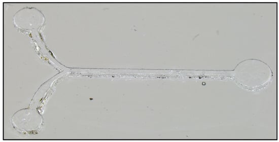
Figure 4.
The intermediate negative master imaged at a slight angle to demonstrate depth and texture. The tiered structure due to the layered substrate is clearly visible along with occasional ablation debris.
2.6. Negative Master Passivation
After removing the intermediate negative master from the positive master, flip over the PDMS to ensure that the features are facing up, and plasma clean the PDMS master for 60 s. Next, place the plasma-activated PDMS master in a plastic petri dish, pour methanol into the container until the PDMS is fully submerged, and degas the PDMS master in a vacuum chamber for 30 min. After removing the passivated PDMS master from the vacuum chamber, discard the excess methanol, place the passivated PDMS master in a glass petri dish, and put it into the oven at 150 °C for 1 min to evaporate any remaining methanol. Note that a plastic petri dish should be used after plasma treatment to prevent bonding between the activated PDMS and glass while a glass petri dish should be used with the oven to prevent thermal deformation of the plastic. This process takes about 35 min. The double casting procedure is shown schematically in Figure 5.
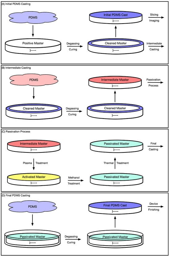
Figure 5.
A schematic illustration of PDMS double casting. (A) The initial positive master is cleaned from fabrication debris by an initial round of PDMS casting. An outer ring of this PDMS layer is left behind to serve as an outer wall for intermediate casting and the central PDMS disk is removed for slicing and imaging of the device profile. (B) PDMS is added to the cleaned positive master for intermediate negative master casting. (C) The intermediate negative master is plasma cleaned and then submerged in methanol in a vacuum chamber. The excess methanol is then discarded and the passivated master is dried in an oven. (D) The passivated negative master is placed into a new petri dish for final PDMS casting.
2.7. Device Casting
After passivation the negative master is ready to be used for casting microfluidic devices. The casting process is the same as before but requires a larger amount of PDMS to give adequate thickness for connecting external tubing. To cast, prepare 44 g of PDMS at a 10:1 ratio of monomer to cross-linker, mix and defoam in the planetary centrifuge, pour over the negative master in a glass petri dish, degas in a vacuum chamber for 20 min to remove air bubbles, remove surface bubbles with a heat gun, cure at 150 °C for 4 min, and allow to cool for 5 min before cutting out the device. This process takes about 30 min. The passivated negative master can be repeatably used to cast additional devices without further modification or re-passivation.
2.8. Device Finishing
To finish the microfluidic device after final casting, first cut out a rectangle of the PDMS which includes all of the device features. To create the input and output connections, place a sampling punch on the connection locations, features side up, and punch the holes through the device. To plasma bond a glass slide to the features side of the PDMS, plasma clean both the glass slide and PDMS device features in a plasma oven for 1 min. Quickly remove the glass slide and PDMS device and press the glass slide onto the PDMS device with the features side touching the glass slide. Next, wrap the device in a paper cloth and clamp it between two glass slides with a binder clip to apply pressure and put the clamped device in the oven at 150 °C for 1 min to allow for a full bond. The microfluidic device is now finished. This final step takes roughly 5 min. The finished device is shown in Figure 6.
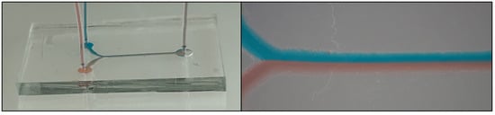
Figure 6.
The finished device with connected tubing and a demonstration of laminar coflow. The finished Y-channel coflow device (left) is connected to syringes of red and blue dye in a syringe pump via flexible tubing, and laminar coflow (right) is clearly visible through a microscope.
3. Results
The “Same Day Microfluidics” fabrication method has been found in practice to be reliable and accessible at a primarily undergraduate institution. Numerous different device variations have been created, and the passivated negative masters have been reused several times without failure. With minimal training and supervision, undergraduate students can be fabricating their own microfluidic devices for use in the laboratory. The timing of each step of this method is shown in Table 1. The only step not listed is mixing the PDMS which can be performed during device design, substrate preparation, or laser cutting. With a planetary centrifuge this takes under 10 min, and the PDMS for every step can be prepared at the same time; for this work the PDMS was mixed while preparing the substrate. A skilled CAD user can create a sketch and generate g-code for the laser cutter in 15 min, but the timing of that step can vary widely. Polyimide substrates can be prepared in 10 min; for this work that was performed while the PDMS was mixing, but substrates could be prepared in advance and ready for use to reduce the timing even further. The process of creating and cleaning the initial positive master takes about 35 min, creating and passivating the negative master takes about 65 min, and casting and finishing the final device takes about 35 min. The total time required is about 160 min, well under three hours. Casting subsequent devices takes about 35 min, not including PDMS preparation.

Table 1.
Timing of each step in the “Same Day Microfluidics” fabrication method. The entire design and fabrication process, from brain to bench, can be achieved in under three hours.
4. Discussion
A key limitation of this method is the minimum feature size which can be created. This work used a 20 W laser module for the Snapmaker A350 which has an elliptical laser spot 80 μm × 100 μm which in practice limits features to at least 150 μm in width. Additional optics or an industrial grade laser cutter could potentially reduce the spot size somewhat, but laser ablation is unlikely to match the <5 μm feature sizes achievable by photolithography. For the vast majority of microfluidic device utilization, this limitation is unlikely to be significant.
Another limitation of this method is the flow channel profile. Due to the Gaussian profile of laser ablation, channels created by laser cutting are highly unlikely to be perfectly rectangular. For the vast majority of microfluidic device utilization, this limitation is unlikely to be significant. If channel profile is a key concern, then xurography (razor writing) may be a better option for initial master fabrication.
A possible limitation of this method is the precise control of channel depth. In practice it was found that the same number of layers of the same polyimide tape did not always result in the same depth of channel. This variation is likely due to variations within the adhesive layer as the nominal combined thickness of the polyimide layer and adhesive layer, 2.4 mil (61 μm), is significantly greater than the measured thickness of one layer of polyimide tape in application, 30 μm, but close to the nominal thickness of the polyimide layer alone, 1 mil (25.4 μm). It could be that the process of spreading the polyimide tape with a razor blade (to prevent trapping air bubbles) is also spreading the adhesive layer. If precise control of channel depth is a key concern, then polyimide film without adhesive may be a better option for substrate preparation.
Curved channels introduce another level of complexity as the laser has been observed to overcut along the direction of the raster path. For the Y-channel device demonstrated here, the raster direction was selected to follow the coflow channel, as shown in Figure 2. Due to this, the curved channels are overcut where the path is perpendicular to the raster path, as can be seen in Figure 3 and Figure 4. The overcutting can be accounted for in the design process by making channels which will be overcut narrower in the original sketch. In Figure 7 this is demonstrated by setting the raster pattern perpendicular to the coflow channel for a narrower channel sketch. Note that this limitation is likely entirely due to the raster pattern being used for the laser path in Luban and may not be an issue with a vector laser path.
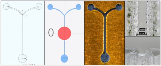
Figure 7.
A demonstration of accounting for laser overcutting in the direction of the laser path. The channel is sketched narrower than the intended final width (far left), and the laser path is set perpendicular the coflow channel (center left). The result is more uniform cutting of the curved paths (center right) and the laser raster pattern is clearly visible in the ablation detritus. Laser cutting perpendicular to the channel results in noticeable scalloping of the walls along the direction of the channel (top right) but does not adversely affect the channel profile (bottom right). Here the channel was sketched with a width of 150 μm, and the bottom of the final channel was measured as 200 μm.
5. Conclusions
This paper presents “Same Day Microfluidics” as a method for the rapid and inexpensive fabrication of microfluidic devices. The traditional method of fabricating microfluidics devices, soft lithography, utilizes photolithography which is an expensive process requiring sophisticated capital intensive equipment. The method presented here avoids photolithography by creating an initial positive master by laser cutting layers of polyimide tape. Functional devices can be cast from an intermediate negative master created using PDMS double casting and passivation. The entire design and fabrication process, from brain to bench, can be achieved in under three hours. Devices created by this method have some limitations regarding the minimum size of features and the profile of the channel, but for most applications of microfluidics these limitations are not likely to be a concern. The fabrication method presented here is accessible to research groups not currently fabricating their own microfluidic devices and as an option for established research groups to more quickly create prototype devices.
Author Contributions
Conceptualization, N.T.; methodology, R.J.A., A.J.S. and N.T.; investigation, R.J.A. and A.J.S.; writing, R.J.A., A.J.S. and N.T. All authors have read and agreed to the published version of the manuscript.
Funding
This project was wholly funded by Wabash College.
Data Availability Statement
Data is contained within the article.
Conflicts of Interest
The authors have no relevant financial or non-financial interests to disclose.
References
- Whitesides, G.M. The origins and the future of microfluidics. Nature 2006, 442, 368–373. [Google Scholar] [CrossRef] [PubMed]
- Xia, Y.; Whitesides, G.M. Soft lithography. Annu. Rev. Mater. Sci. 1998, 28, 153–184. [Google Scholar] [CrossRef]
- Duffy, D.C.; McDonald, J.C.; Schueller, O.J.; Whitesides, G.M. Rapid prototyping of microfluidic systems in poly (dimethylsiloxane). Anal. Chem. 1998, 70, 4974–4984. [Google Scholar] [CrossRef]
- Thompson, L.F. An Introduction to Lithography; ACS Publications: Washington, DC, USA, 1983. [Google Scholar]
- Richter, K.; Orfert, M.; Howitz, S.; Thierbach, S. Deep plasma silicon etch for microfluidic applications. Surf. Coatings Technol. 1999, 116, 461–467. [Google Scholar] [CrossRef]
- Klank, H.; Kutter, J.P.; Geschke, O. CO2-laser micromachining and back-end processing for rapid production of PMMA-based microfluidic systems. Lab Chip 2002, 2, 242–246. [Google Scholar] [CrossRef]
- Patko, D.; Mártonfalvi, Z.; Kovacs, B.; Vonderviszt, F.; Kellermayer, M.; Horvath, R. Microfluidic channels laser-cut in thin double-sided tapes: Cost-effective biocompatible fluidics in minutes from design to final integration with optical biochips. Sens. Actuators B Chem. 2014, 196, 352–356. [Google Scholar] [CrossRef]
- Isiksacan, Z.; Guler, M.T.; Aydogdu, B.; Bilican, I.; Elbuken, C. Rapid fabrication of microfluidic PDMS devices from reusable PDMS molds using laser ablation. J. Micromech. Microeng. 2016, 26, 035008. [Google Scholar] [CrossRef]
- Bartholomeusz, D.A.; Boutté, R.W.; Andrade, J.D. Xurography: Rapid prototyping of microstructures using a cutting plotter. J. Microelectromechanical Syst. 2005, 14, 1364–1374. [Google Scholar] [CrossRef]
- Cosson, S.; Aeberli, L.G.; Brandenberg, N.; Lutolf, M.P. Ultra-rapid prototyping of flexible, multi-layered microfluidic devices via razor writing. Lab Chip 2015, 15, 72–76. [Google Scholar] [CrossRef]
- Martínez-López, J.I.; Mojica, M.; Rodríguez, C.A.; Siller, H.R. Xurography as a rapid fabrication alternative for point-of-care devices: Assessment of passive micromixers. Sensors 2016, 16, 705. [Google Scholar] [CrossRef]
- Wilson, M.E.; Kota, N.; Kim, Y.; Wang, Y.; Stolz, D.B.; LeDuc, P.R.; Ozdoganlar, O.B. Fabrication of circular microfluidic channels by combining mechanical micromilling and soft lithography. Lab Chip 2011, 11, 1550–1555. [Google Scholar] [CrossRef] [PubMed]
- Chen, P.C.; Zhang, R.H.; Chen, L.T. Using micromachined molds, partial-curing PDMS bonding technique, and multiple casting to create hybrid microfluidic chip for microlens array. Micromachines 2019, 10, 572. [Google Scholar] [CrossRef] [PubMed]
- Javidanbardan, A.; Azevedo, A.M.; Chu, V.; Conde, J.P. A systematic approach for developing 3D high-quality PDMS microfluidic chips based on micromilling technology. Micromachines 2021, 13, 6. [Google Scholar] [CrossRef] [PubMed]
- Lee, D.K.; Kwon, J.Y.; Cho, Y.H. Fabrication of microfluidic channels with various cross-sectional shapes using anisotropic etching of Si and self-alignment. Appl. Phys. A 2019, 125, 291. [Google Scholar] [CrossRef]
- Walsh, D.I.; Kong, D.S.; Murthy, S.K.; Carr, P.A. Enabling microfluidics: From clean rooms to makerspaces. Trends Biotechnol. 2017, 35, 383–392. [Google Scholar] [CrossRef]
- Li, H.F.; Lin, J.M.; Su, R.G.; Cai, Z.W.; Uchiyama, K. A polymeric master replication technology for mass fabrication of poly (dimethylsiloxane) microfluidic devices. Electrophoresis 2005, 26, 1825–1833. [Google Scholar] [CrossRef]
- Tompkins, N.; Cambria, M.C.; Wang, A.L.; Heymann, M.; Fraden, S. Creation and perturbation of planar networks of chemical oscillators. Chaos Interdiscip. J. Nonlinear Sci. 2015, 25, 064611. [Google Scholar] [CrossRef]
- Carugo, D.; Lee, J.Y.; Pora, A.; Browning, R.J.; Capretto, L.; Nastruzzi, C.; Stride, E. Facile and cost-effective production of microscale PDMS architectures using a combined micromilling-replica moulding (μ Mi-REM) technique. Biomed. Microdevices 2016, 18, 4. [Google Scholar] [CrossRef]
- Koerner, T.; Brown, L.; Xie, R.; Oleschuk, R.D. Epoxy resins as stamps for hot embossing of microstructures and microfluidic channels. Sens. Actuators B Chem. 2005, 107, 632–639. [Google Scholar] [CrossRef]
- Li, S.; Van Nguyen, S.; Lee, B.K. Role of heat treatment in improving replication quality of PDMS double-casting. Soft Matter 2022, 18, 3473–3478. [Google Scholar] [CrossRef]
- Yang, L.; Hao, X.; Wang, C.; Zhang, B.; Wang, W. Rapid and low cost replication of complex microfluidic structures with PDMS double casting technology. Microsyst. Technol. 2014, 20, 1933–1940. [Google Scholar] [CrossRef]
- Ansari, A.; Trehan, R.; Watson, C.; Senyo, S. Increasing silicone mold longevity: A review of surface modification techniques for PDMS-PDMS double casting. Soft Mater. 2021, 19, 388–399. [Google Scholar] [CrossRef]
- Gitlin, L.; Schulze, P.; Belder, D. Rapid replication of master structures by double casting with PDMS. Lab Chip 2009, 9, 3000–3002. [Google Scholar] [CrossRef]
- Hassanin, H.; Jiang, K. Multiple replication of thick PDMS micropatterns using surfactants as release agents. Microelectron. Eng. 2011, 88, 3275–3277. [Google Scholar] [CrossRef]
- Briones, M.P.P.; Honda, T.; Yamaguchi, Y.; Miyazaki, M.; Nakamura, H.; Maeda, H. A practical method for rapid microchannel fabrication in polydimethylsiloxane by replica molding without using silicon photoresist. J. Chem. Eng. Jpn. 2006, 39, 1108–1114. [Google Scholar] [CrossRef]
- Zhuang, G.; Kutter, J.P. Anti-stiction coating of PDMS moulds for rapid microchannel fabrication by double replica moulding. J. Micromech. Microeng. 2011, 21, 105020. [Google Scholar] [CrossRef]
- Shao, G.; Wu, J.; Cai, Z.; Wang, W. Fabrication of elastomeric high-aspect-ratio microstructures using polydimethylsiloxane (PDMS) double casting technique. Sens. Actuators A Phys. 2012, 178, 230–236. [Google Scholar] [CrossRef]
- Ziółkowska, K.; Żukowski, K.; Chudy, M.; Dybko, A.; Brzózka, Z. Enhancing efficiency of double casting prototyping by thermal aging of poly (dimethylsiloxane). In Proceedings of the Proc, MicroTAS, Seattle, WA, USA, 2–6 October 2011. [Google Scholar]
- Kwapiszewska, K.; Żukowski, K.; Kwapiszewski, R.; Brzózka, Z. Double casting prototyping with a thermal aging step for fabrication of 3D microstructures in poly (dimethylsiloxane). AIMS Biophys. 2016, 3, 553–562. [Google Scholar] [CrossRef]
- Javidanbardan, A.; Chu, V.; Conde, J.P.; Azevedo, A.M. Microchromatography integrated with impedance sensor for bioprocess optimization: Experimental and numerical study of column efficiency for evaluation of scalability. J. Chromatogr. A 2022, 1661, 462678. [Google Scholar] [CrossRef]
- Kim, S.H.; Lee, S.; Ahn, D.; Park, J.Y. PDMS double casting method enabled by plasma treatment and alcohol passivation. Sens. Actuators B Chem. 2019, 293, 115–121. [Google Scholar] [CrossRef]
- Cherry, B.; Orcutt, A.; Tompkins, N. Comparison of Double Casting Methods for Microfluidic Device Fabrication. Preprints 2024. [CrossRef]
- Sung, J.; So, H. Facile and cost-effective PDMS double-casting method based on curing temperature and ratio for solvent detecting applications. Sens. Actuators B Chem. 2023, 387, 133834. [Google Scholar] [CrossRef]
Disclaimer/Publisher’s Note: The statements, opinions and data contained in all publications are solely those of the individual author(s) and contributor(s) and not of MDPI and/or the editor(s). MDPI and/or the editor(s) disclaim responsibility for any injury to people or property resulting from any ideas, methods, instructions or products referred to in the content. |
© 2025 by the authors. Licensee MDPI, Basel, Switzerland. This article is an open access article distributed under the terms and conditions of the Creative Commons Attribution (CC BY) license (https://creativecommons.org/licenses/by/4.0/).