1. Introduction
In recent years, DC/DC converters have been broadly used in numerous fields such as renewable energy systems, electric vehicles, DC microgrids and industrial applications. Electrical energy generated by renewable energy sources, especially from photovoltaic technology, has gained more attention and hence become the most important renewable source to meet the energy challenges increasing day by day. Photovoltaics solar systems are non-linear, as the magnitude of voltage and current produced by PV varies with weather conditions such as solar irradiance and temperature. Therefore, these systems require converters that have wide input voltage range, higher voltage gain, high power range and improved efficiency. In renewable energy sources, specifically in photovoltaics systems, DC/DC converters play vital roles and have more significance. PV voltage is not constant and varies due to its non-linear behavior, and to resolve this problem, these converters are required. The main objective of these converters is to supply constant output voltage irrespective of the variation in the input voltage generated by the PV. To satisfy the requirements of a high voltage conversion ratio, high power range and good efficiency, there are many step-up DC/DC converter topologies reported in the literature [
1,
2,
3,
4].
Isolated DC/DC converters are transformer-based converter topologies. For high-power applications, these converters can attain significantly high voltage gain and high efficiency. However, this type of converter topology has some problems that limits its application for photovoltaic systems. Isolated converters have magnetizing elements and require galvanic isolation through a low- or high-frequency transformer, through which the size, weight, losses and expense of the power converter are all raised. Therefore, isolated DC/DC converters are typically neglected for solar PV system, and to minimize the size and weight and maximize the overall efficiency of the converters, preference is given to non-isolated converters, which are transformer-less converters.
Quadratic boost converter topologies of transformer-less converters have been presented in the literature, but they have high switch voltage and require additional filter capacitors and inductors, which makes these topologies complex [
5]. Cascaded interconnection topologies of the basic boost and buck–boost converters have been reported, and efficiency of these converters drops due to their series connections [
6]. Transformer-less converters such as boost, buck–boost, buck, SEPIC, Cuk and zeta converters are broadly used for PV applications. Reviews of these converters are presented in [
7,
8]. Still, however, the choice of a specific DC/DC converter has become a hard task, and research is being carried out for designing converters for PV application. DC/DC converters deployed with a solar system should have simple design, a low number of components, low input voltage ripple and low output voltage ripple and be cost effective. Chow and Tse presented non-cascaded converter configuration in [
9], and they introduced the concepts of reduced redundant power processing. All the reduced redundant power processing configurations lead to high voltage gain and have better efficiency, but in [
10], the authors investigated the I-IIB buck–boost/boost configuration of R2P2 converters for waste heat recovery system for a ship. This topology is selected here for further analysis for PV system.
This paper includes the analysis of I-IIB buck–boost/boost non-isolated converter configuration for a photovoltaic system, which has never been investigated for a PV system before in the literature. The proposed converter working principal will be discussed. Mathematical modeling of the converter will be carried out for a 3 Kw PV system. Selection of suitable switching frequency and its impact on switching loss for the converter will be discussed. Analysis of the converter for efficiency evaluation considering ideal and parasitic elements will be discussed and validate the results of theoretical curves and simulations. Switch loss and overall converter loss are also discussed, and at the end, a conclusion is made.
2. Proposed Converter and Working Principal
The proposed converter’s power circuit for PV applications is shown in
Figure 1. The proposed converter topology I-IIB buck–boost/boost is a non-isolated converter. The proposed converter has a simple design and low number of switching components. The converter consists of PV panels, power input voltage source, two inductors (
,
), two transistors (MOSFETs switch
,
), two diodes, load and two capacitors, of which one is used as storage element, referred to as the output capacitor, and the other is used as a buffer capacitor to reduce the over-voltages and oscillations. For symmetric function of the converter, analysis was made with the two inductors, which are of the same value, and at the same time, both MOSFET switches were turned on, fired with the same duty cycle.
The working principle of topology is as follows: when both the switches are turned on, then both inductors named , start charging in parallel from PV DC source. The power demanded by the load is supplied by the output capacitor, which is used as energy storage element. When switches are switched off, then both inductors are linked in series through diodes and start releasing their energy to the output capacitor and the load.
3. Mathematical Modelling of the Proposed Topology
By using the theoretical calculations and design parameters, the converter topology for 3 kW was modeled in MATLAB to show the theoretical behavior of the converter. The mathematical equations for the converter analysis are as follows.
Equation for voltage gain is given below:
where
D is the duty cycle required to maintain the constant output voltage. The PV panels power
Vin is an ideal voltage source.
Duty cycle is obtained from above equation to have a specific voltage gain.
Average inductor current can be calculated from Equation (3).
The equation for calculating the inductor value is given below:
The design parameters of topology for PV application are given in
Table 1.
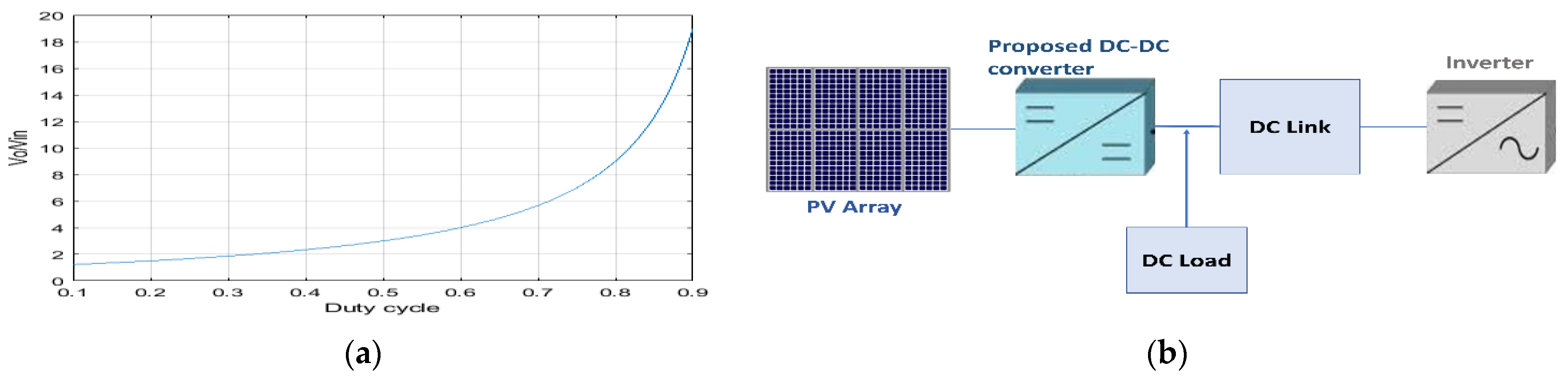
Figure 2a,b shows the theoretical characteristic curve for duty cycle related to step-up voltage ratio for PV application and block diagram of converter integrated with PV, respectively. The curve shows that a very small duty cycle is needed to achieve the desired step-up voltage gain and to maintain constant 400 Vdc at the output of the converter, for a typical DC link input voltage for inverter in PV system.
4. Simulations and Results
For the analysis of converter for PV application, a 3 kW prototype of proposed converter was designed in PSIM software. The converter was designed to operate well with wide input voltage range and to maintain constant 400 V at the output. SiC power MOSFETs model C3M0030090K were used to have improved efficiency. Diodes used were power Schottky SiC diode model STPSC20065.
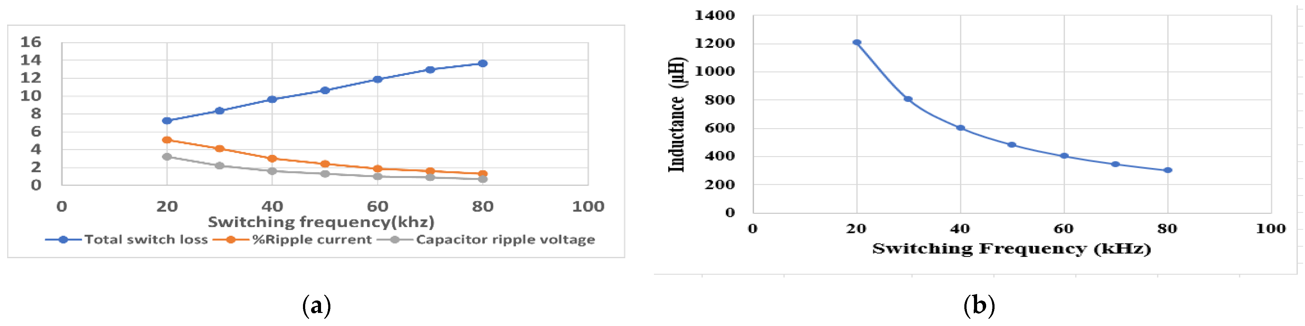
Switching frequency plays a vital role in the overall efficiency of a converter. Therefore, analysis for the selection of suitable switching frequency must be performed. To evaluate this, the converter was simulated for
Vin = 150 V with different frequency levels. Simulation results for different switching frequency related to switch loss, inductor ripple current and capacitor ripple voltage are shown in
Figure 3a.
Figure 3b shows the inductance value for specific switching frequencies.
Results show that by increasing the switching frequency, switch loss gradually increases. Inductor ripple current and capacitor ripple voltage decrease. Therefore, by considering all these scenarios from the graph, we concluded that 50 kHz switching frequency is the most suitable, due to appearing in the middle and being acceptable in term of losses and ripples. Hence, switching frequency 50 kHz was selected for the converter.
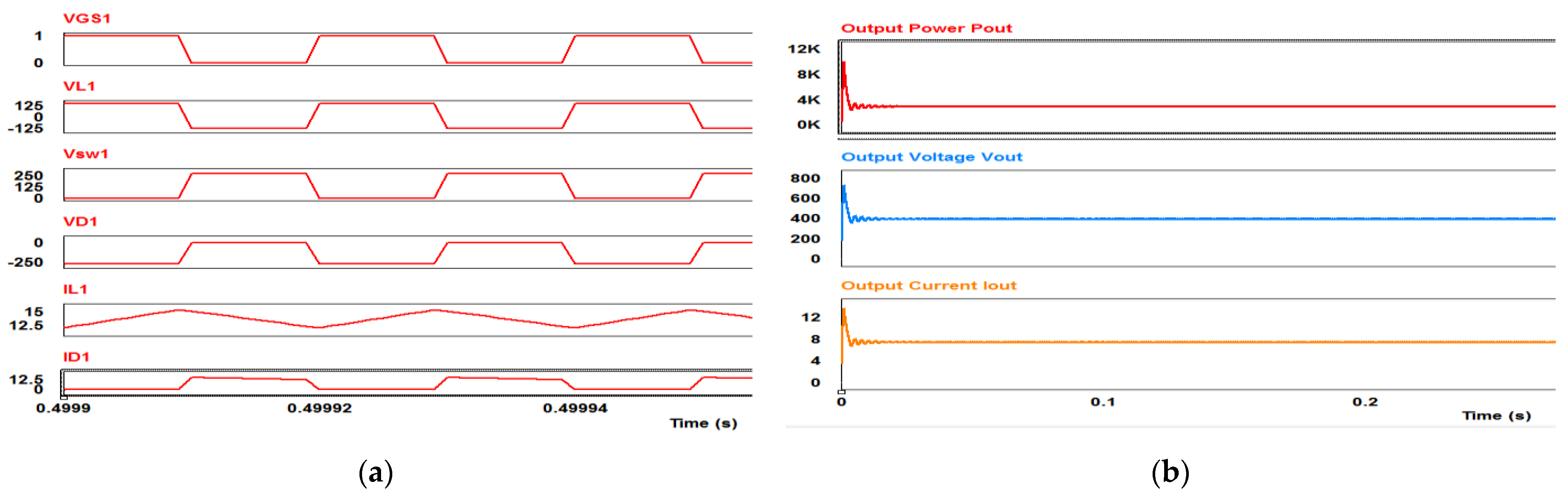
Figure 4a,b shows the voltage and current stresses on converter components and 3 KW output power of the designed converter, output voltage and current at load side, respectively.
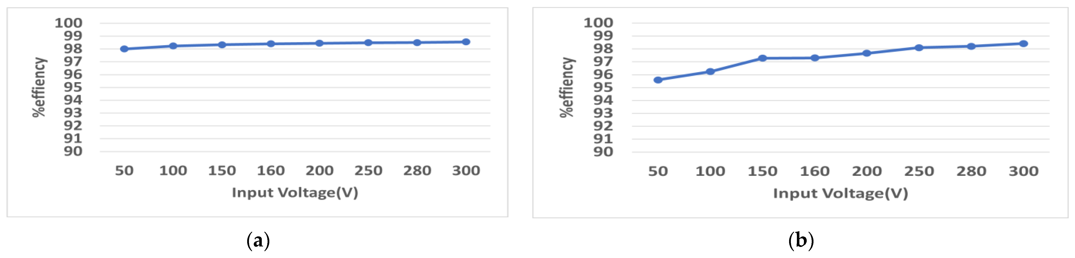
Figure 5a shows the simulated result of topology considering ideal elements. Results show that as we increase the input voltage of converter, its efficiency also increases, as it requires a small duty cycle to achieve specific voltage gain.
Figure 5b shows the influence of parasitic elements on the efficiency of the whole converter. With parasitic elements, efficiency drops down compared with ideal efficiency, validating the influence of parasitic elements on the converter.
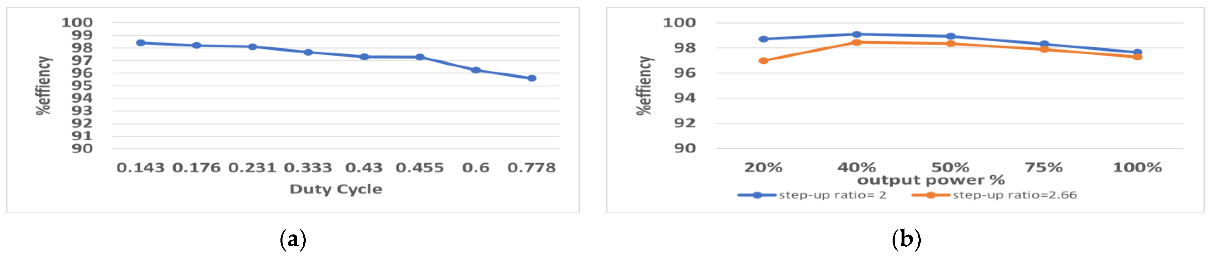
Figure 6a shows the efficiency of the converter for the whole range of duty cycle for PV application. Results show that efficiency drops down with an increase in duty cycle because of high stress on switching devices. Results also show that efficiency is above 97%,a which is good enough for a PV system. In
Figure 6b, a graph compares efficiency and variable output power for step-up ratios 2 and 2.66. Results show that the converter can operate at high frequency for different step-up ratios and a high-power range.
In
Figure 7a,b, a graph shows the power loss due to switching device (MOSFET) for a wide input voltage range. Results show that with an increase in voltage level, conduction losses are gradually decreasing due to small duty cycle, but switching losses increase linearly with increase in input voltage.
5. Conclusions
In this paper, analysis of I-IIB buck–boost/boost non-isolated reduced redundant power processing converter configuration is presented to evaluate its efficiency and reliability for a PV system both theoretically and by simulations. The converter is operating well in CCM mode. Results show that if we use this converter for PV application, a small duty cycle range is required to achieve the desired step-up ratio and constant output voltage. Simulations of the 3 kW prototype for the efficiency evaluation were conducted with wide input voltage range. The converter shows high efficiency for a wide input voltage range and at high duty cycle. From results and efficiency analysis, this converter topology seems to be more reliable and suitable for high-power application.
Author Contributions
Conceptualization, S.A.S. and H.A.K.; methodology, S.A.S. and H.A.K.; software, S.A.S.; validation, S.A.S., H.A.K. and H.F.; formal analysis, S.A.S.; investigation, S.A.S.; resources, S.A.S.; data curation, S.A.S.; writing—original draft preparation, S.A.S.; writing—review and editing, S.A.S. and H.F.; visualization, S.A.S.; supervision, S.A.S. and H.A.K.; project administration, S.A.S.; funding acquisition, S.A.S. All authors have read and agreed to the published version of the manuscript.
Funding
This research received no external funding.
Conflicts of Interest
The authors declare no conflict of interest.
References
- Allehyani, A. Analysis of a symmetrical multilevel DC-DC boost converter with ripple reduction structure for solar PV systems. Alex. Eng. J. 2022, 61, 7055–7056. [Google Scholar] [CrossRef]
- Purushothaman, S.K.; Sattianadan, D.; Vijayakumar, K. Novel compact design high gain DC–DC step up converter applicable for PV applications. Sustain. Energy Technol. Assess. 2022, 51, 101720. [Google Scholar] [CrossRef]
- Raghavendra, K.V.G.; Zeb, K.; Muthusamy, A.; Krishna, T.N.V.; Prabhudeva Kumar, S.V.S.V.; Kim, D.-H.; Kim, M.-S.; Cho, H.-G.; Kim, H.-J. A comprehensive review of DC–DC converter topologies and modulation strategies with recent advances in solar photovoltaic systems. Electronics 2020, 9, 31. [Google Scholar] [CrossRef] [Green Version]
- Forouzesh, M.; Siwakoti, Y.P.; Gorji, S.A.; Blaabjerg, F.; Lehman, B. Step-up DC–DC converters: A comprehensive review of voltage-boosting techniques, topologies, and applications. IEEE Trans. Power Electron. 2017, 32, 9143–9178. [Google Scholar] [CrossRef]
- Leyva-Ramos, J.; Mota-Varona, R.; Ortiz-Lopez, M.G.; Diaz-Saldierna, L.H.; Langarica-Cordoba, D. Control strategy of a quadratic boost converter with voltage multiplier cell for high-voltage gain. IEEE J. Emerg. Sel. Top. Power Electron. 2017, 5, 1761–1770. [Google Scholar] [CrossRef]
- Matsuo, H.; Harada, K. The cascade connection of switching regulators. IEEE Trans. Ind. Appl. 1976, IA-12, 192–198. [Google Scholar] [CrossRef]
- Taghvaee, M.H.; Radzi, M.A.M.; Moosavain, S.M.; Hizam, H.; Marhaban, M.H. A current and future study on non-isolated DC–DC converters for photovoltaic applications. Renew. Sustain. Energy Rev. 2013, 17, 216–227. [Google Scholar] [CrossRef]
- Ghasemi, A.; Eilaghi, S.F.; Adib, E. A new non-isolated high step-up SEPIC converter for photovoltaic applications. In Proceedings of the 2012 3rd Power Electronics and Drive Systems Technology (PEDSTC), Tehran, Iran, 15–16 February 2012; IEEE: Piscataway, NJ, USA, 2012; pp. 51–56. [Google Scholar]
- Tse, C.K.; Chow, M.H.; Cheung, M.K. A family of PFC voltage regulator configurations with reduced redundant power processing. IEEE Trans. Power Electron. 2001, 16, 794–802. [Google Scholar] [CrossRef] [Green Version]
- Zogogianni, C.G.; Tatakis, E.C.; Porobic, V. Investigation of a non-isolated reduced redundant power processing DC/DC converter for high-power high step-up applications. IEEE Trans. Power Electron. 2018, 34, 5229–5242. [Google Scholar] [CrossRef]
| Publisher’s Note: MDPI stays neutral with regard to jurisdictional claims in published maps and institutional affiliations. |
© 2022 by the authors. Licensee MDPI, Basel, Switzerland. This article is an open access article distributed under the terms and conditions of the Creative Commons Attribution (CC BY) license (https://creativecommons.org/licenses/by/4.0/).


