Abstract
With the growth of renewable energy sources around the world, the demand for cost-effective and efficient converters that can operate at high frequency and have less switching and conduction loss has grown. High efficiency is one of the most difficult goals to attain in power electronic converters. Wideband switches can be used to achieve this purpose, although they add to the system’s cost. In this paper, a comparison between SiC MOSFET and Si MOSFET switches was carried out for a 3 KW I-IIB Buck-boost/Boost non-isolated reduced redundant converter for the photovoltaic system with a wide input voltage range. Mathematical calculations were used to investigate switching and conduction losses, and software simulations in PSIM were used to verify their authenticity. In high-frequency power applications, the results suggest that SiC MOSFET can work more efficiently than Si MOSFET. Si MOSFETs, on the other hand, are still preferred for small voltage and low power applications due to their lower costs.
1. Introduction
Renewable energy sources are rapidly used all around the world due to its plentiful, environment-friendly, and broadly distributed nature. Renewable energy sources, specifically solar energy, have gained more attention and become the most important source to meet energy challenges. The energy produced from PV systems is non-linear because the magnitude of voltage and current coming from PV varies due to weather conditions such as temperature and solar irradiance. Thus, these systems require converters that will provide a constant output, be able to work with a wide input voltage range, possess a high power range, and have high efficiency. In renewable energy sources specifically for photovoltaics systems, DC/DC converters have more significance and play a vital role. Due to the non-linear behavior of PV systems, DC/DC converters are necessary for them. The basic goal of a DC/DC converter is to provide smooth and constant output voltage with great efficiency regardless of the input voltage generated by PV panels [1,2].
In the selection and design of converters, efficiency is a critical consideration. Most commercially available converters are constructed on silicon devices. Switching devices play important role in converter designing. There are two types of switching devices SiC and Si MOSFETs mainly used for power converters. Si MOSFETs are widely used as switching devices due to their low cost but SiC MOSFETs have gained more attention in the last few years due to their high efficiency, ability to work with high temperature and frequency, and high-power density [3]. Hence, the loss analysis of switching devices should be evaluated for converters and accompanies the low switching loss device.
In the literature, various types of converter topologies have been proposed for reducing losses; however, this has increased the amount of switches and the total complication of the system [4]. SiC and Si MOSFETs are the primary switching devices of converters. When compared to Si switches, wide bandgap switching devices such as silicon carbide switches are able to perform better with high power, high frequency, and high voltage applications. The loss comparison of SiC and Si MOSFET for half bridge LLC converters is reported in [5,6]. The efficiency, size, and power density of various Silicon carbide MOSFETs are compared in [7]. In comparison to Si MOSFETs, it is proposed that SiC MOSFETs can function at higher frequencies with improved efficiency [8,9,10].
This paper includes an analysis of the I-IIB Buck-boost/Boost non-isolated reduced redundant power-processing converter with a Si MOSFET compared to a model with a SiC MOSFET. Conduction and switching losses were simulated and calculated using the simulation software PSIM for a wide input voltage range, and both versions were compared under various loads; conduction and switching losses were calculated.
2. Proposed Converter
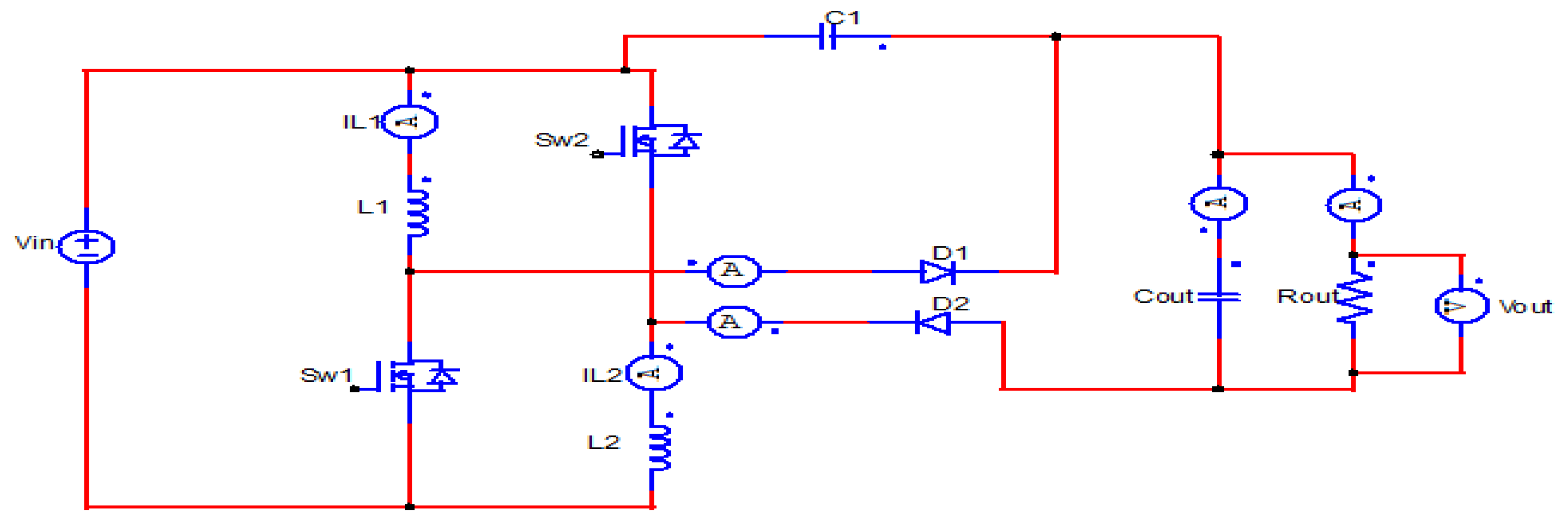
The proposed topology is the “I-IIB Buck-boost/Boost reduced redundant power-processing converter” for PV applications, as shown in Figure 1. The design parameters of topology for PV application are given in Table 1. The proposed converter has a simpler design and the lowest number of switching components. The converter consists of the input voltage source, two inductors ( and ), two transistors (MOSFETs switch and ), two diodes, load, and two capacitors from which one is used as the storage element referred to the output capacitor, and other is used as a buffer capacitor to reduce the overvoltages and oscillations. The working principle of topology is that when both the switches are turned on, then both inductors named and start charging in parallel from dc source. The power demanded by load is supplied by the output capacitor.
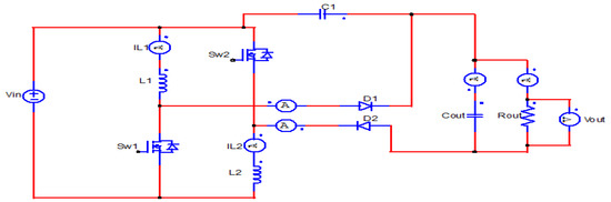
Figure 1.
Proposed converter for the PV system.

Table 1.
Design parameter of the proposed converter.
In this paper, a 3 KW I-IIB Buck-boost/Boost non-isolated reduced redundant converter is modeled for Si MOSFET (STW45NM50) and SiC MOSFET (C3M0030090K) to evaluate their functioning. The proposed converter works with varied input voltage ranges and the converter output is controlled by adjusting the duty cycle. Table 2 shows a comparison of Si (STW45NM50) and SiC (C3M0030090K) MOSFETs. At high temperatures, SiC MOSFETs have a better reverse-charge recovery characteristic. The cost of Si MOSFET, on the other hand, is significantly cheaper than that of a SiC MOSFET.
Table 2.
SiC MOSFET compared to Si MOSFET.
3. Mathematical Modelling of the Proposed Topology
Mathematical computations are used to estimate MOSFET losses. In both of our suggested models, Equations (1)–(7) are utilized to calculate losses across all MOSFETs [7].
Input Current:
Average current for converter:
Approximate RMS current:
Peak Current:
Conduction losses across each MOSFET:
Switching Losses for one MOSFET:
Total Losses for all MOSFETS:
Here, the SiC MOSFET-C3M0030090K is utilized for one model and the Si MOSFET-STW45NM50 is used for another. Only one operation mode is investigated, with the duty ratio kept constant, to highlight the difference in components.
4. Simulations and Results
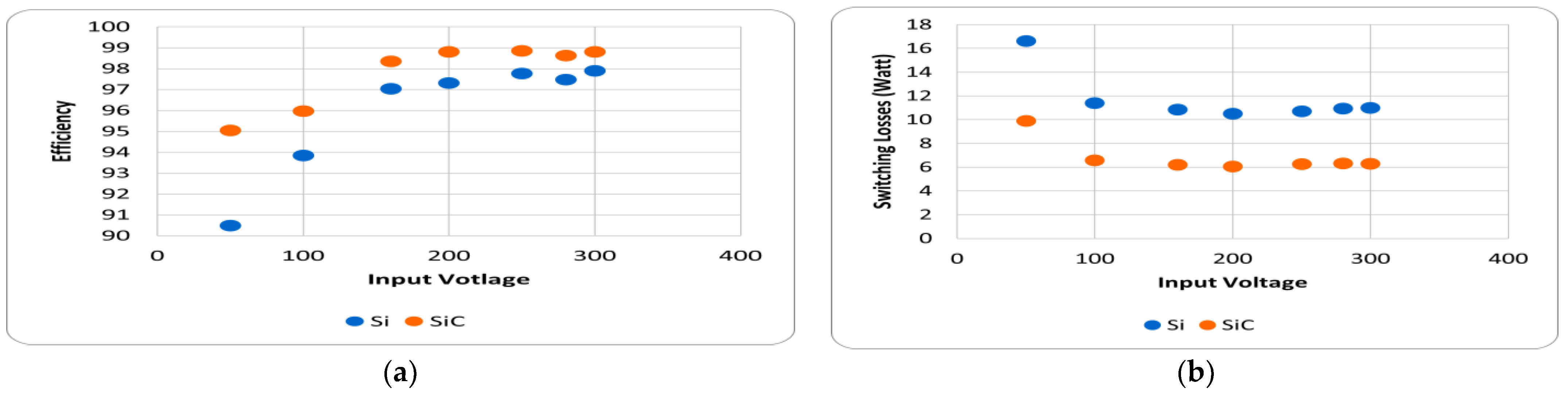
For the analysis of converter for PV applications, a 3 kW prototype of the proposed converter is constructed for both models in PSIM software. SiC MOSFET- C3M0030090K is used for one prototype and Si MOSFET-STW45NM50 is used for another prototype. The converter is designed to operate well with a wide input voltage range and maintains a constant 400 V at the output. The PSIM simulation model of I-IIB Buck-boost/Boost reduced redundant power-processing converter is shown in Figure 2. Figure 3a shows the efficiency of the converter for a wide input voltage range for both the Si and SiC MOSFETs. The result shows that the efficiency of Si MOSFET is low compared to SiC MOSFET. Figure 3b shows the switching loss for changes in the input voltage. The result shows that the SiC MOSFET’s switching loss is lower than the Si MOSFET’s switching loss.
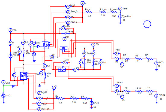
Figure 2.
PSIM simulation model of I-IIB Buck-boost/Boost reduced redundant power-processing converter.
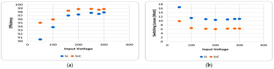
Figure 3.
(a) Efficiency analysis of converter for different input voltages; (b) switching loss with changes in input voltage.
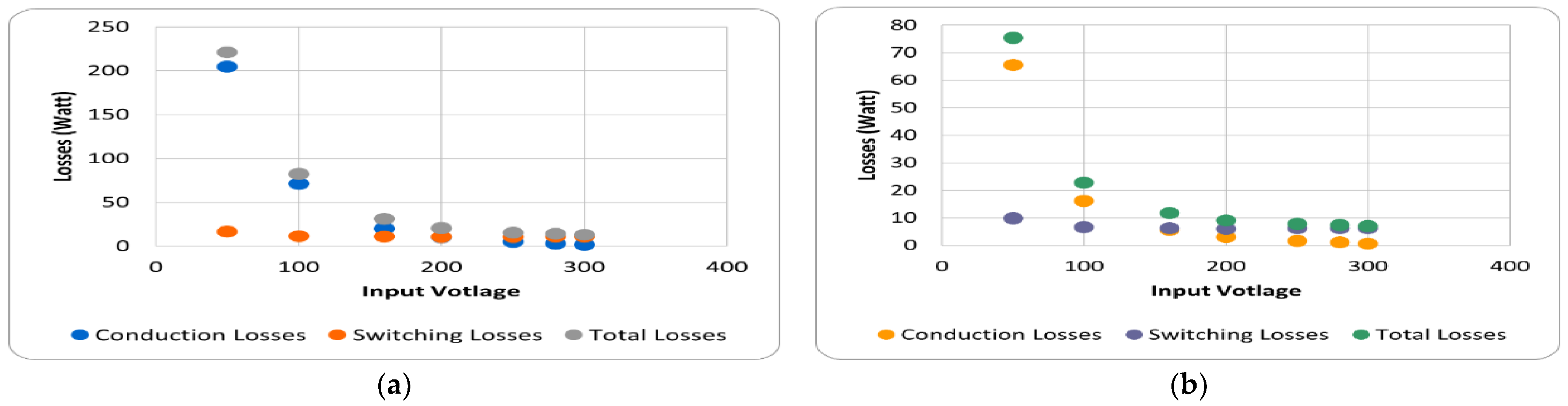
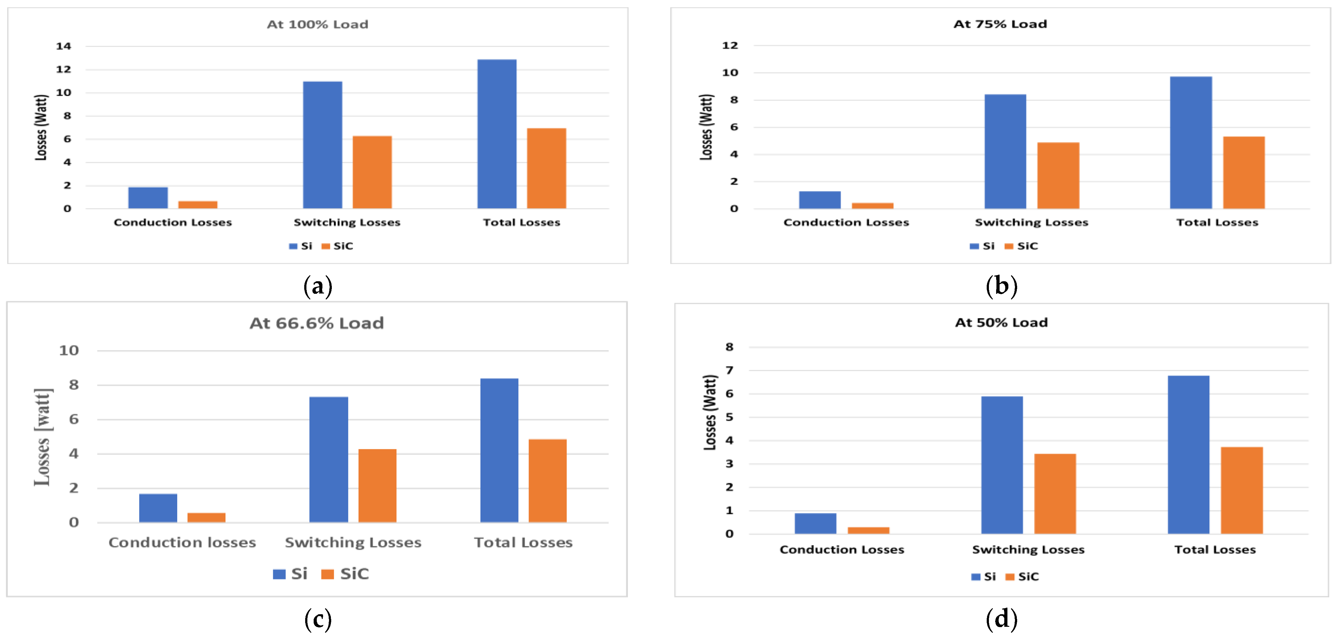
Figure 4a,b show switching and conduction loss for Si and SiC MOSFETS with different input voltages. The result show that as we increase the input voltage, the switching loss also increases. At low inputs, voltage conduction loss is high. The switching loss of SiC MOSFETs is much lower than Si MOSFET’s. Figure 5a–d show the loss comparison of switches at different power levels for full loads at 75%, 66.6%, and 50% load. SiC MOSFETs have substantially lower switching and conduction losses than Si MOSFETs.
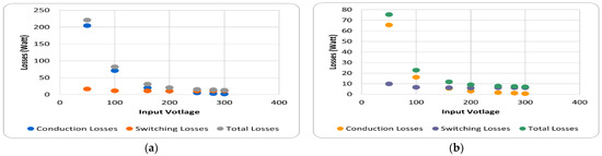
Figure 4.
(a) Loss analysis of Si MOSFETs with change in input voltages; (b) loss analysis of SiC MOSFETs for input voltages.
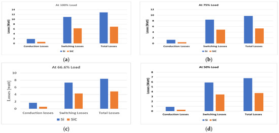
Figure 5.
(a) Comparison of loss for Si and SiC at full load (3 KW); (b) comparison of loss Si and SiC at 75% load (2.25 KW); (c) comparison of loss Si and SiC at 66.6% load (2 KW); (d) comparison of loss Si and SiC at 50% load (1.5 KW).
5. Conclusions
In this paper, an analysis of the I-IIB Buck-boost/Boost non-isolated reduced redundant converter for Si (STW45NM50) and SiC (C3M0030090K) MOSFETs is designed in this study. Si and SiC properties were compared. PSIM was used to simulate switching and conduction losses. The findings were compared across a wide input voltage range, switching frequency, and for power. The findings reveal that silicon carbide (SiC) MOSFETs are more efficient in high-frequency power applications than silicon (Si) MOSFETs. Si MOSFETs, on the other hand, are still preferred in low-voltage and low-power applications due to their lower costs.
Author Contributions
Conceptualization, S.A.S. and H.A.K.; methodology, S.A.S. and H.A.K.; software, S.A.S.; validation, S.A.S., H.A.K. and H.F.; formal analysis, S.A.S.; investigation, S.A.S.; resources, S.A.S.; data curation, S.A.S.; writing—original draft preparation, S.A.S.; writing—review and editing, S.A.S. and H.F.; visualization, S.A.S.; supervision, S.A.S. and H.A.K.; project administration, S.A.S.; funding acquisition, S.A.S. All authors have read and agreed to the published version of the manuscript.
Funding
This research received no external funding.
Conflicts of Interest
The authors declare no conflict of interest.
References
- Allehyani, A. Analysis of a symmetrical multilevel DC-DC boost converter with ripple reduction structure for solar PV systems. Alex. Eng. J. 2022, 61, 7055–7065. [Google Scholar] [CrossRef]
- Raghavendra, K.V.G.; Zeb, K.; Muthusamy, A.; Krishna, T.N.V.; Kumar, S.V.P.; Kim, D.H.; Kim, M.S.; Cho, H.G.; Kim, H.J. A comprehensive review of DC–DC converter topologies and modulation strategies with recent advances in solar photovoltaic systems. Electronics 2020, 9, 31. [Google Scholar] [CrossRef] [Green Version]
- Pandey, P.; Agnihotri, P. An Efficient LLC Resonant Converter Design for Photovoltaic Application. In Proceedings of the 2019 8th International Conference on Power Systems (ICPS), Jaipur, India, 20–22 December 2019. [Google Scholar]
- Aghdam, M.G.H.; Thiringer, T. Comparison of SiC and Si power semiconductor devices to be used in 2.5 kW DC/DC converter. In Proceedings of the 2009 International Conference on Power Electronics and Drive Systems (PEDS), Taipei, Taiwan, 2–5 November 2009. [Google Scholar]
- Van den Bossche, A.; Stoyanov, R.; Dukov, N.; Valchev, V.; Marinov, A. Analytical simulation and experimental comparison of the losses in resonant DC/DC converter with Si and SiC switches. In Proceedings of the 2016 IEEE International Power Electronics and Motion Control Conference (PEMC), Varna, Bulgaria, 25–28 September 2016. [Google Scholar]
- Farooq, H.; Khalid, H.A.; Ali, W.; Shahid, I. A Comparative Analysis of Half-Bridge LLC Resonant Converters Using Si and SiC MOSFETs. Eng. Proc. 2021, 12, 43. [Google Scholar] [CrossRef]
- Sarriegui, G.; Beushausen, S.; De Doncker, R.W. Performance comparison of different SiC-MOSFETs for high-frequency high-power DC-DC converters. In Proceedings of the 2017 IEEE 8th International Symposium on Power Electronics for Distributed Generation Systems (PEDG), Florianopolis, Brazil, 17–20 April 2017. [Google Scholar]
- Han, D.; Noppakunkajorn, J.; Sarlioglu, B. Efficiency comparison of SiC and Si-based bidirectional DC-DC converters. In Proceedings of the 2013 IEEE Transportation Electrification Conference and Expo (ITEC), Detroit, MI, USA, 16–19 June 2013. [Google Scholar]
- Farooq, H.; Khalid, H.A.; Khalid, M.U.; Farooqi, M.M.; Malik, Q. Loss Analysis of Full Bridge LLC Resonant Converter with Wide Input Range Using Si and SiC Switches. In Proceedings of the 2021 16th International Conference on Emerging Technologies (ICET), Islamabad, Pakistan, 22–23 December 2021. [Google Scholar]
- Daranagama, T.; Udrea, F.; Logan, T.; McMahon, R. A performance comparison of SiC and Si devices in a bi-directional converter for distributed energy storage systems. In Proceedings of the 2016 IEEE 7th International Symposium on Power Electronics for Distributed Generation Systems (PEDG), Vancouver, BC, Canada, 27–30 June 2016. [Google Scholar]

Publisher’s Note: MDPI stays neutral with regard to jurisdictional claims in published maps and institutional affiliations. |
© 2022 by the authors. Licensee MDPI, Basel, Switzerland. This article is an open access article distributed under the terms and conditions of the Creative Commons Attribution (CC BY) license (https://creativecommons.org/licenses/by/4.0/).