

Proceeding Paper

Development of Dielectrophoresis Electrodes for Nanowire Alignment †
James Watt School of Engineering, University of Glasgow, Glasgow G12 8QQ, UK
*
Authors to whom correspondence should be addressed.
Presented at the International Conference on Responsible Electronics and Circular Technologies (REACT 2025), Glasgow, UK, 11–12 November 2025.
Eng. Proc. 2026, 127(1), 9; https://doi.org/10.3390/engproc2026127009
Published: 11 March 2026

Abstract

This work presents the design and simulation of DEP electrodes with an interdigitated electrode (IDE) pattern for the alignment of 1D nanostructures using COMSOL simulations. The impact of electric field distribution with varying electrode geometry, voltage, and frequency were studied using these simulations. The maximum electric field value of 2.6 × 10⁶ V/m was observed at electrode edges and gaps. Moreover, a significant increase in the electric field was observed with a decrease in finger width. These simulation results for DEP electrodes have huge potential in advancing 1D nanowire-based flexible and wearable electronic devices in the future.

1. Introduction

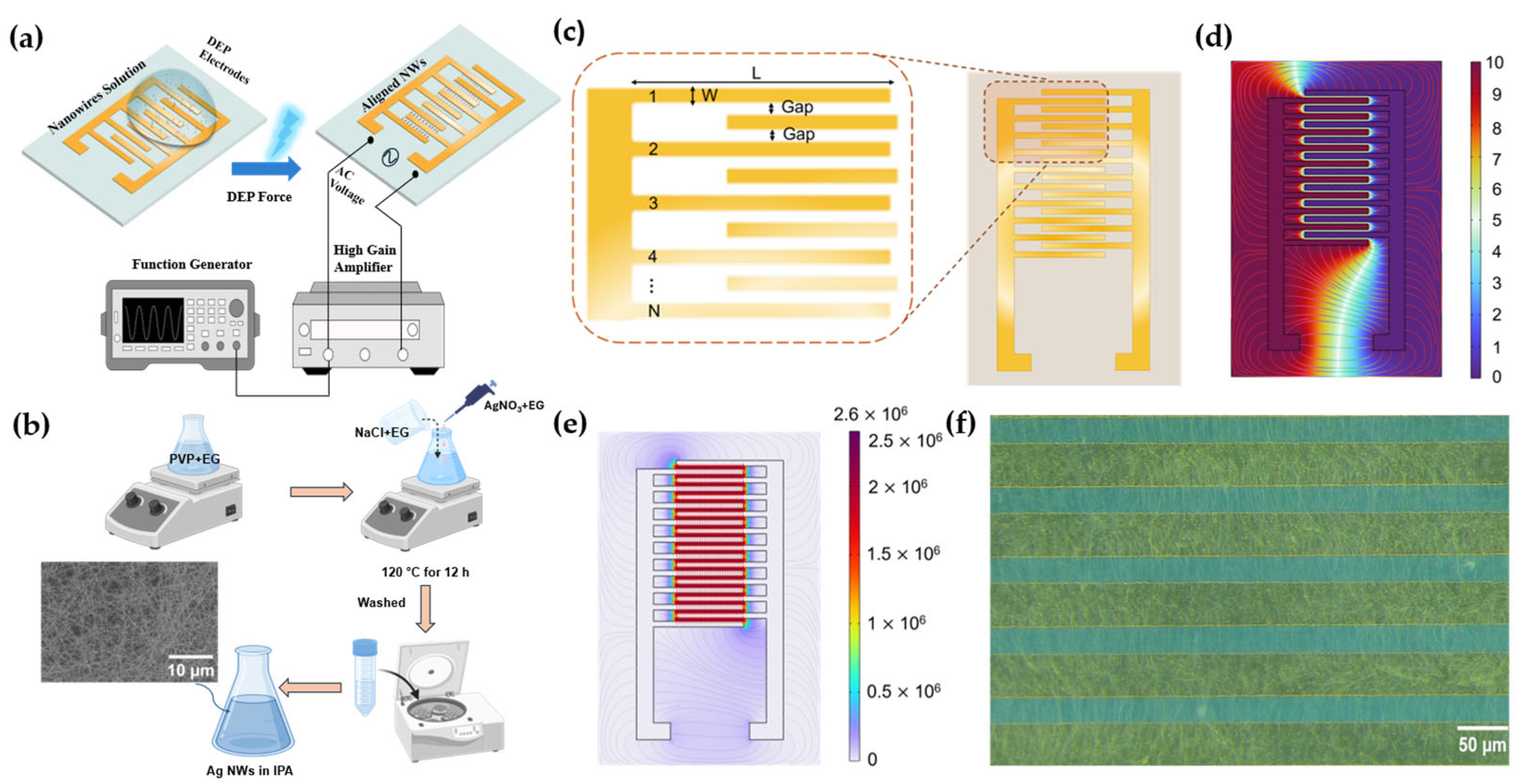
Recently, 1D nanostructures like nanowires (NWs), nanotubes, and nanorods offer unique optical, electrical, and mechanical properties and hold huge potential for various applications, including sensors and memristors [1,2]. To fully exploit the versatile properties of nanowires, it is critical to have precise control over the alignment of NWs in desired shapes and angles through the application of strong electric fields. DEP is a versatile technique used to precisely align nanowires by applying a non-uniform external electric field that induces a strong dipole moment inside the nanowires [2,3,4]. Under external non-uniform external stimuli, electrical charges are redistributed inside the NWs, resulting in an electric dipole moment inside the liquid medium. This technique involves the alignment of the NWs into a desired shape and direction through the application of a high alternating current (AC) voltage between the planar electrodes under a dielectric medium [4,5,6]. Further, the DEP technique is highly precise in terms of alignment (orientations and positions), versatile with, for example, metallic, semiconductors, and dielectric materials, and very beneficial for future 1D nanowire-based gate-all-around/multi-gated transistors like FinFET, double-gated FETs, transparent conducting electrodes, and various other nanoscale devices. A schematic representation of NW alignment using DEP is shown in Figure 1a.
The optimization of key parameters, such as the applied voltage, electrode design, and geometry, is crucial for the precise and effective alignment of NW into the desired positions and angles [3,4]. This systematic study provides deep insights into the design of DEP electrodes along with the fundamental transport properties of the 1D nanostructures [6]. Also, the DEP technique is a promising and versatile technique for aligning different types of 1D nanomaterials to manufacture high-performance and large-area nanowire-based flexible and wearable sensors and transistors.

2. Methodology

The polyol method was used to prepare Ag NWs because it is a simple, cost-effective processing method [7,8,9]. In typical Ag NW synthesis, three solutions are prepared: solution 1 (S1): 500 mg of AgNO3 in 20 mL of ethylene glycol (EG); S2: 116.8 mg of NaCl in 20 mL of EG; S3: 400 mg of PVP (36,000 MW) in 20 mL of EG. Then, 10 mL of EG, 2 mL of solution 2, and 10 mL of solutions 1 and 3 are added into a 100 mL conical flask. The solution was stirred for 20 min at 10,000 r/min, room temperature. Next, the conical flask was kept on a preheated hotplate at 120 °C for 12 h. The procedure is depicted in Figure 1b.

3. Results and Discussion

The NWs dispersed in solvents like IPA, DI, and water and were attracted by DEP forces toward regions with high electrical field gradients. This nanowire alignment is mainly due to the electrical polarization of dielectric particles in a non-uniform electrical field created by the DEP electrodes. To study the effect of DEP force on the alignment or orientation of NWs, a nanowire was modelled as cylindrical particles, with the DEP expression is defined in Equation (1) [10]:
F D E P = π r 2 l 6 ε m R e ε p * ε m * ε p * + 2 ε m * E 2
where E is the electric field, r and l are the radius and length of the cylindrical particle, and ε p * and ε m * denote the complex permittivity of the particle and medium. Equation (1) reveals that the DEP force depends significantly on the electric field gradient and magnitude, resulting in high DEP forces in regions with high electric field [4]. Therefore, it is crucial to study the effect of the generated electric field on the electrode to effectively manipulate the nanowires.
In this study, a regular IDE with various geometrical parameters, such as the width and length of the electrode fingers, the gap between adjacent fingers, and the number of finger pairs, was investigated as part of a preliminary study of DEP forces. Figure 1c presents a schematic of the designed planar DEP electrode along with enlarged geometric parameters. Gold was chosen as the electrode material due to its high conductivity (electrical conductivity σ = 4.5 × 10⁷ S, relative permittivity: 1), and the medium was set to air. The electrode was simulated and analyzed using the AC/DC module in COMSOL Multiphysics V6.2. By applying an AC electric potential of 10 Vpp at a frequency of 10 kHz across the two parallel terminals of the electrode, the generated maximum electrical field was 2.6 × 10⁶ V/m. Figure 1d,e illustrate the electric potential and electric field distribution over the electrode in the medium. It can be observed that the maximum electric field values, in the range of 106 V/m, were generated at the electrode edges and gaps. Figure 1f shows aligned Ag NWs on electrodes using optimized parameters. The average length and diameter of the synthesized Ag NWs were calculated to be 31 µm and 85 nm.
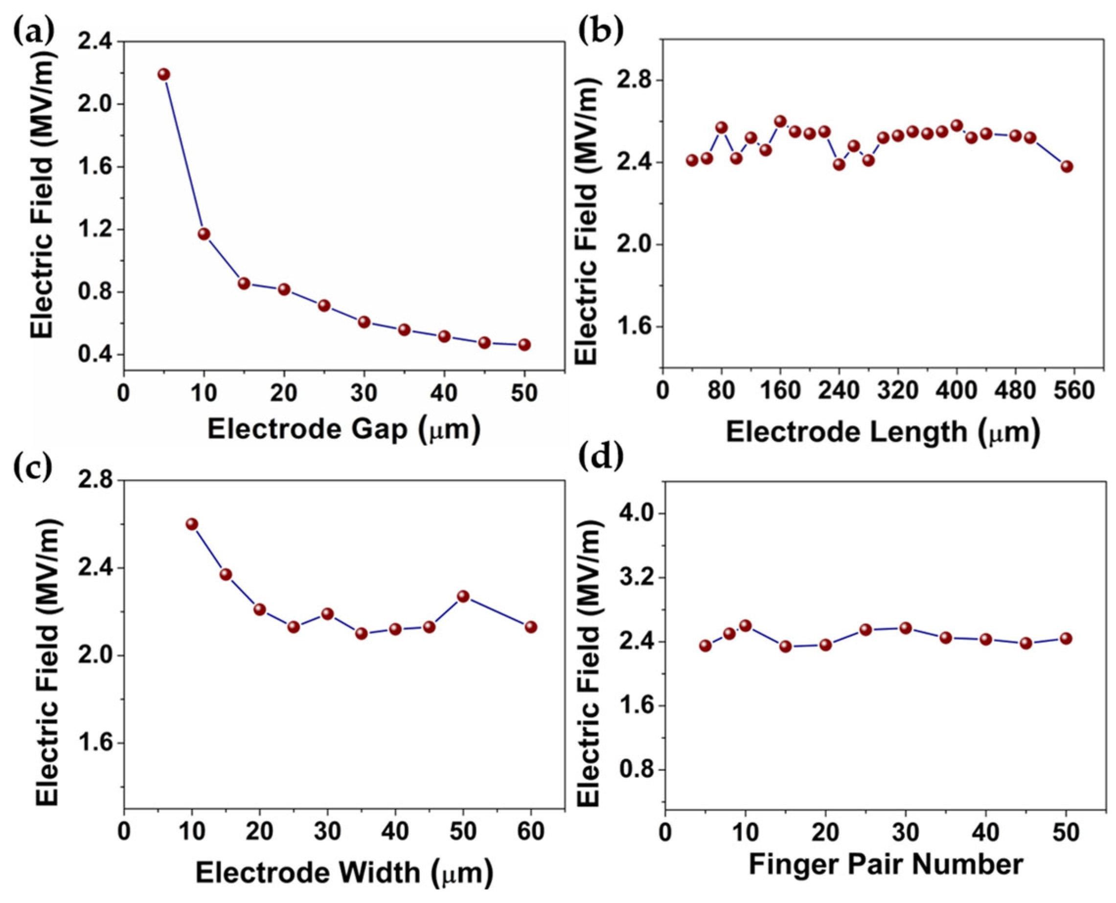
The simulation results of the electric field distribution as a function of different geometric parameters of the electrode are shown in Figure 2a–d. The initial design of the electrode features 10 pairs of fingers and a 10 μm electrode width. Figure 2a shows that the electric field varies with the electrode gap size from 5 to 60 μm and that the peak magnitude of the electrical field is generated at the smallest gap size of 5 μm. Additionally, the width of the electrode finger strongly affects the electric field generation over the electrodes, following the trend that smaller widths can generate higher electric fields, as seen in Figure 2c. In comparison, finger length and the number of finger pairs did not show a significant influence on the magnitude of the electric field. As illustrated in Figure 2b,d, the maximum value occurs when the number of fingers is 10 and the electrode length is 160 μm, with the electrode fingers separated by 5 μm.

4. Conclusions

In this study, we successfully demonstrated the design and simulation of DEP electrodes using COMSOL simulation. These DEP electrodes were explored for the alignment of 1D nanostructures. These simulations revealed the effect of geometry, applied voltage, and frequency on the DEP force. A reliable method was proposed for the precise alignment of these 1D nanostructures through optimization studies, which will be very useful in our subsequent experimental studies. The DEP electrodes generate a maximum electric field of 106 V/m for an electrode spacing of 5 μm. Further, uniform, and long silver nanowires were successfully synthesized using the polyol method. This study’s simulation results will be used for the fabrication of the electrodes, and the synthesized nanowires will be further explored in subsequent DEP experiments.

Author Contributions

Conceptualization, J.Z., V.S. and B.P.Y.; methodology J.Z., V.S. and B.P.Y.; software, J.Z.; data curation, J.Z., V.S. and B.P.Y.; validation, J.Z., V.S. and B.P.Y.; writing—original draft preparation, J.Z., V.S. and B.P.Y.; supervision, M.A. and H.H. All authors have read and agreed to the published version of the manuscript.

Funding

The authors acknowledge support from our funding body of Engineering and Physical Sciences Research council (EPSRC) under project number (EP/W025752/1).

Institutional Review Board Statement

Not applicable.

Informed Consent Statement

Not applicable.

Data Availability Statement

The original contributions presented in this study are included in the article. Further inquiries can be directed to the corresponding authors.

Acknowledgments

The authors thank the staff of the James Watt Nanofabrication Centre (JWNC) for their support during the experimental and fabrication processes involved in this study.

Conflicts of Interest

The authors declare no conflicts of interest.

References

  1. Amjadi, M.; Pichitpajongkit, A.; Lee, S.; Ryu, S.; Park, I. Highly stretchable and sensitive strain sensor based on silver nanowire–elastomer nanocomposite. ACS Nano 2014, 8, 5154–5163. [Google Scholar] [CrossRef] [PubMed]
  2. Wu, X.; Cui, N.; Zhang, Q.; Xiong, X.; Zhu, T.; Xu, Q. ZnO Single-Nanowire Schottky Barrier Resistive Switching Memory Assembly with Dielectrophoresis. J. Electron. Mater. 2022, 51, 7190–7197. [Google Scholar] [CrossRef]
  3. Chen, Y.; Liang, T.; Chen, L.; Chen, Y.; Yang, B.R.; Luo, Y.; Liu, G.S. Self-assembly, alignment, and patterning of metal nanowires. Nanoscale Horiz. 2022, 7, 1299–1339. [Google Scholar] [CrossRef] [PubMed]
  4. Pethig, R. Review—Where Is Dielectrophoresis (DEP) Going? J. Electrochem. Soc. 2017, 164, B3049. [Google Scholar] [CrossRef]
  5. Dimaki, M.; Bøggild, P. Dielectrophoresis of carbon nanotubes using microelectrodes: A numerical study. Nanotechnology 2004, 15, 1095. [Google Scholar] [CrossRef]
  6. Dos Santos, M.V.P.; Béron, F.; Pirota, K.R.; Diniz, J.A.; Moshkalev, S. Electrical manipulation of a single nanowire by dielectrophoresis. In Nanowires—New Insights; IntechOpen: London, UK, 2017; pp. 41–58. [Google Scholar]
  7. Fu, D.; Yang, R.; Wang, Y.; Wang, R.; Hua, F. Silver nanowire synthesis and applications in composites: Progress and prospects. Adv. Mater. Technol. 2022, 7, 2200027. [Google Scholar] [CrossRef]
  8. Kumar, A.; Kumar, M.; Goyat, M.S.; Avasthi, D.K. A review of the latest developments in the production and applications of Ag-nanowires as transparent electrodes. Mater. Today Commun. 2022, 33, 104433. [Google Scholar] [CrossRef]
  9. Shi, Y.; Fang, J. Large-scale synthesis of high-purity silver nanowires with reduced diameters by the polyethylene glycol-assisted polyol method. J. Phys. Chem. C 2022, 126, 19866–19871. [Google Scholar] [CrossRef]
  10. Jones, T.B. Electromechanics of Particles; Cambridge University Press: Cambridge, UK, 1995. [Google Scholar]
Figure 1. Schematics illustrating (a) NW alignment using DEP; (b) DEP electrode design, including finger length (L), finger width (W), and gap between parallel electrode pairs; (c) electric potential distribution after applying 10 Vpp; (d) normalized electric field distribution, where red arrows indicate electric field vectors; (e) synthesis of Ag NWs using polyol method; (f) aligned Ag NWs on IDE pattern (Au/Glass).
Engproc 127 00009 g001
Figure 2. The normalized electric field over the proposed electrode varies with different electrode geometric parameters: (a) electric field versus electrode gap, (b) electric field versus electrode length, (c) electric field versus electrode width, and (d) electric field versus number of fingers.
Engproc 127 00009 g002
Disclaimer/Publisher’s Note: The statements, opinions and data contained in all publications are solely those of the individual author(s) and contributor(s) and not of MDPI and/or the editor(s). MDPI and/or the editor(s) disclaim responsibility for any injury to people or property resulting from any ideas, methods, instructions or products referred to in the content.